

Datasheet CY8C27143, CY8C27243, CY8C27443, CY8C27543, CY8C27643 Datasheet (Cypress Semiconductor)
Page 1
PSoC® Programmable System-on-Chip
CY8C27143, CY8C27243
CY8C27443, CY8C27543, CY8C27643
Features
DIGITAL SYSTEM
SRAM
256 Bytes
Interrupt
Controller
Sleep and
Watchdog
Multiple Clock Sources
(Inc ludes I MO, I LO, PLL, and E CO)
Global Digital Interconnect
Global Analog Interconnect
PSoC
CORE
CPU Core (M8C)
SROM Flash 16K
Digital
Block
Array
Multiply
Accum.
Switch
Mod e
Pump
Internal
Voltage
Ref.
Digital
Clocks
POR and LVD
System Resets
Decimator
SYSTEM RESOURCES
ANALOG SYSTEM
Analog
Ref.
Analog
Input
Muxing
I C
2
Por t 4 Por t 3 Por t 2 Por t 1 Port 0
Analog
Drivers
System Bus
Analog
Block
Array
Por t 5
Logic Block Diagram
■
Powerful Harvard Architecture Processor
❐
M8C processor speeds to 24 MHz
❐
8x8 multiply, 32-bit accumulate
❐
Low power at high speed
❐
3.0 to 5.25V operating voltage
❐
Operating voltages down to 1.0V using on-chip switch mode
pump (SMP)
❐
Industrial temperature range: -40°C to +85°C
■
Advanced Peripherals (PSoC® Blocks)
❐
12 rail-to-rail analog PSoC blocks provide:
• Up to 14-Bit ADCs
• Up to 9-Bit DACs
• Programmable Gain Amplifiers
• Programmable filters and comparators
❐
Eight digital PSoC blocks provide:
• 8- to 32-bit timers, counters, and PWMs
• CRC and PRS modules
• Up to two full-duplex UARTs
• Multiple SPI™ Masters or Slaves
• Connectable to all GPIO pins
❐
Complex peripherals by combining blocks
■
Precision, Programmable Clocking
❐
Internal 2.5% 24/48 MHz oscillator
❐
24/48 MHz with optional 32 kHz crystal
❐
Optional external oscillator, up to 24 MHz
❐
Internal oscillator for watchdog and sleep
■
Flexible On-Chip Memory
❐
16K Flash program storage 50,000 erase/write cycles
❐
256 bytes SRAM data storage
❐
In-System Serial Programming (ISSP)
❐
Partial Flash updates
❐
Flexible protection modes
❐
EEPROM emulation in Flash
■
Programmable Pin Configuratio n s
❐
25 mA Sink, 10 mA Source on all GPIO
❐
Pull up, pull down, high Z, strong, or open drain drive modes
on all GPIO
❐
Eight standard analog inputs on GPIO, plus four additional
analog inputs with restricted routing
❐
Four 30 mA analog outputs on GPIO
❐
Configurable interrupt on all GPIO
■
Additional System Resources
❐
I2C slave, master, and multi-master to 400 kHz
❐
Watchdog and sleep timers
❐
User-configurable low voltage detection
❐
Integrated supervisory circuit
❐
On-chip precision voltage reference
■
Complete Development T ools
❐
Free development software (PSoC Designer™)
❐
Full featured, In-Circuit Emulator and Programmer
❐
Full speed emulation
❐
Complex breakpoint structure
❐
128K trace memory
Cypress Semiconductor Corporation • 198 Champion Court • San Jose,CA 95134-1709 • 408-943-2600
Document Number: 38-12012 Rev. *O Revised November 20, 2009
[+] Feedback
Page 2

CY8C27143, CY8C27243
CY8C27443, CY8C27543, CY8C27643
Contents
Features ............................................................................... 1
Logic Block Diagram ....................................... ...................1
Contents .............................................................................. 2
PSoC Functional Overview ................................................3
PSoC Core ....................................................................3
Digital System ...............................................................3
Analog System ................................................... ... ........4
Additional System Resources .......................................5
PSoC Device Characteristics ........................................5
Getting Started ....................................................................5
Application Notes ..........................................................5
Development Kits .................................................. ........5
Training .........................................................................5
CYPros Consultants ......................................................5
Solutions Library ............................................................5
Technical Support .........................................................5
Development Tools ............................................................6
PSoC Designer Software Subsystems ..........................6
In-Circuit Emulator .........................................................6
Designing with PSoC Designer .........................................7
Select Components .......................................................7
Configure Components .................................................7
Organize and Connect ..................................................7
Generate, Verify, and Debug .........................................7
Document Conventions ................................................... ..8
Acronyms Used .............................................................8
Units of Measure ...........................................................8
Numeric Naming .............................................. ... ...........8
Pinouts ................................................................................9
8-Pin Part Pinout ..........................................................9
20-Pin Part Pinout ........................................................9
28-Pin Part Pinout ......................................................10
44-Pin Part Pinout ......................................................11
48-Pin Part Pinout .......................................................12
56-Pin Part Pinout .......................................................14
Register Reference .................................................... .. .....16
Register Conventions ..................................................16
Register Mapping Tables ............................................16
Electrical Specifications ..................................... ... ..........19
Absolute Maximum Ratings .........................................20
Operating Temperature ..............................................20
DC Electrical Characteristics .......................................21
AC Electrical Characteristics .......................................32
Packaging Information .....................................................41
Packaging Dimensions ................................................41
Thermal Impedances ........................................ ..........46
Capacitance on Crystal Pins ......................................46
Solder Reflow Peak Temperature ...............................47
Development Tool Selection ...........................................48
Software ......................................................................48
Development Kits ........................................................48
Evaluation Tools ..........................................................48
Device Programmers ...................................................49
Accessories (Emulation and Programming) ..................49
Third-Party Tools .........................................................49
Build a PSoC Emulator into Your Board ......................49
Ordering Information ........................................................50
Ordering Code Definitions ..........................................51
Document History Page ..................................................52
Sales, Solutions, and Legal Information ........................53
Worldwide Sales and Design Support .........................53
Products ......................................................................53
Document Number: 38-12012 Rev. *O Page 2 of 53
[+] Feedback
Page 3
CY8C27143, CY8C27243
CY8C27443, CY8C27543, CY8C27643
PSoC Functional Overview
DIGITAL SYSTEM
To System Bus
D
i
g
i
t
a
l
C
l
o
c
k
s
F
r
o
m
C
o
r
e
Digita l PS oC Block A rray
To Analog
System
8
Row Input
Configuration
Row Output
Configuration
88
8
Row 1
DBB10 DBB11 DCB12 DCB13
Row Input
Configuration
4
4
Row Output
Configuration
Row 0
DBB00 DBB01 DCB02 DCB03
4
4
GI E[7:0]
GIO[7:0]
GOE[7:0]
GOO [7:0]
Global Digital
Interconnect
Por t 4
Por t 3
Por t 2
Por t 1
Por t 0
Port 5
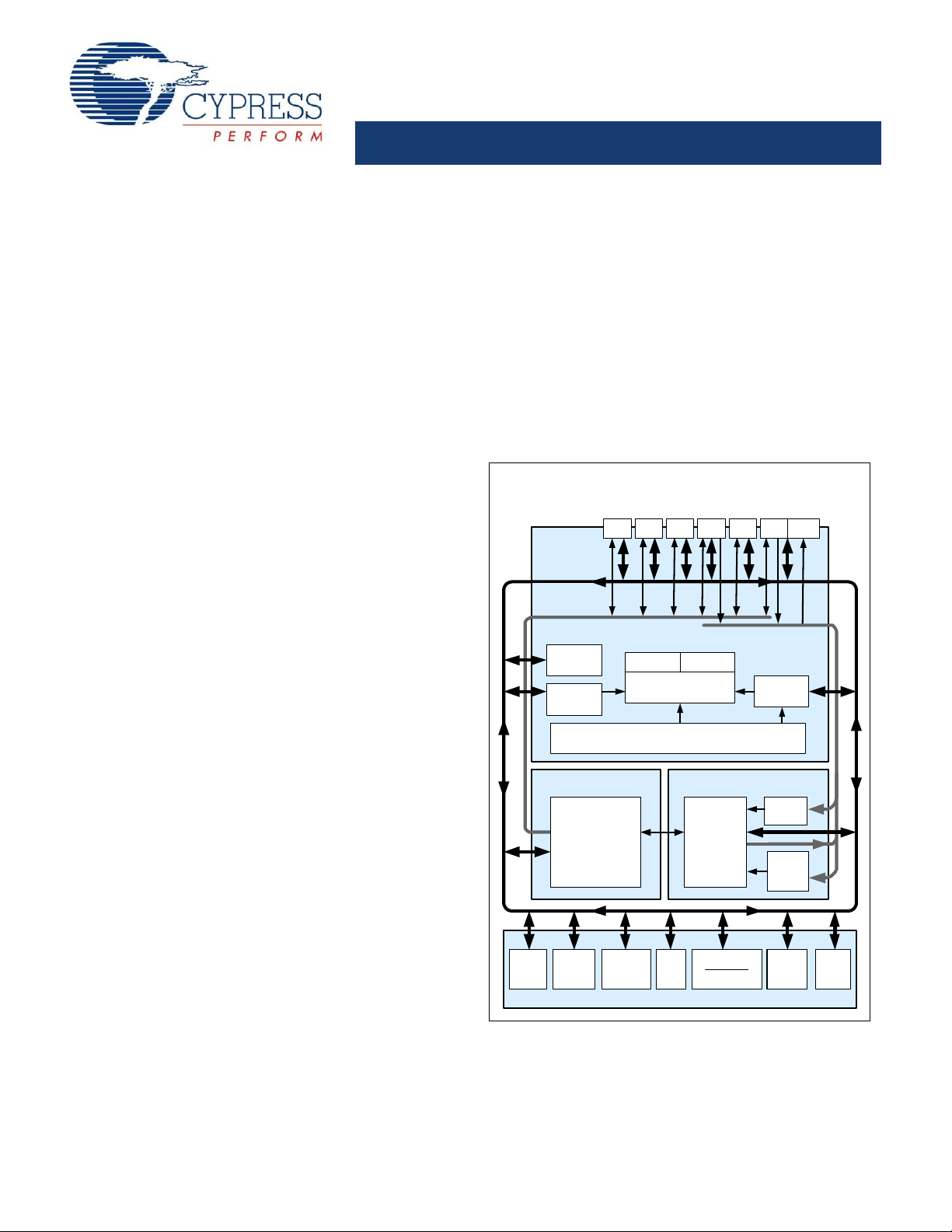
The PSoC family consists of many Programmable
System-on-Chip Controller devices. These devices are designed
to replace multiple traditional MCU-based system components
with one, low cost single-chip programmable device. PSoC
devices include configurable blocks of analog and digital logic,
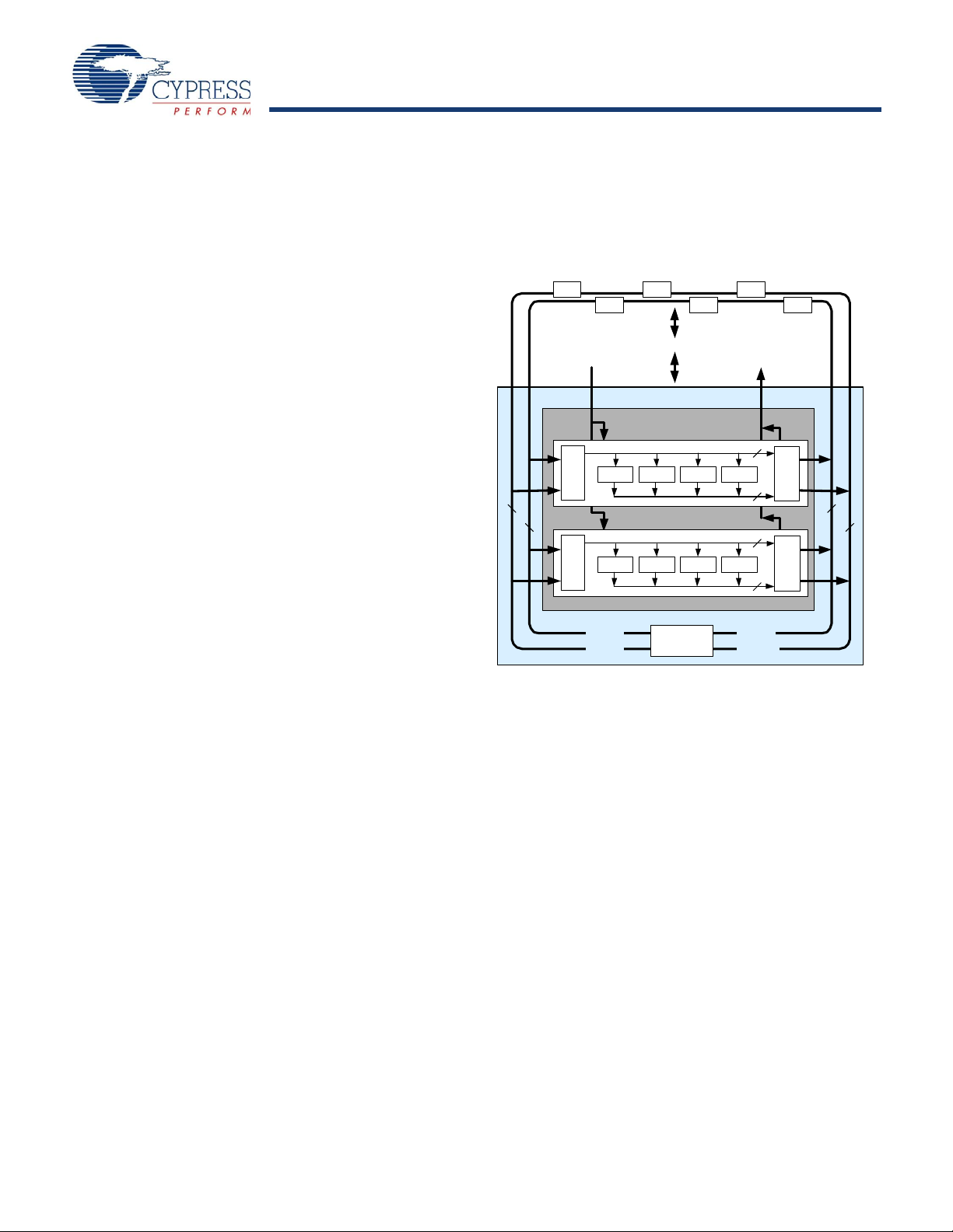
Digital System
The Digital System is composed of 8 digital PSoC blocks. Each
block is an 8-bit resource that can be used alone or combined
with other blocks to form 8, 16, 24, and 32-bit peripherals, which
are called user module references.
Figure 1. Digital System Block Diagram
as well as programmable interconnects. This architecture allows
the user to create customized peripheral configurations that
match the requirements of each individual application.
Additionally, a fast CPU, Flash program memory, SRAM data
memory, and configurable I/O are included in a range of convenient pinouts and packages.
The PSoC architecture, as illustrated on the left, is comprised of
four main areas: PSoC Core, Digital System, Analog System,
and System Resources. Configurable global busing allows all
the device resources to be combined into a complete custom
system. The PSoC CY8C27x43 family can have up to five I/O
ports that connect to the global digital and analog interconnects,
providing access to 8 digital blocks and 12 analog blocks.
PSoC Core
The PSoC Core is a powerful engine that supports a rich feature
set. The core includes a CPU, memory , clocks, and configurable
GPIO (General Purpose I/O).
The M8C CPU core is a powerful processor with speeds up to 24
MHz, providing a four MIPS 8-bit Harvard architecture microprocessor. The CPU utilizes an interrupt controller with 17 vectors,
to simplify programming of real time embedded events. Program
execution is timed and protected using the included Sle ep and
Watch Dog Timers (WDT).
Memory encompasses 16K of Flash for program storage, 256
bytes of SRAM for data storage, and up to 2K of EEPROM
emulated using the Flash. Program Flash utilizes four protection
levels on blocks of 64 bytes, allowing customized software IP
protection.
The PSoC device incorporates fl exible internal clock generators,
including a 24 MHz IMO (internal main oscillator) accurate to
2.5% over temperature and voltage. The 24 MHz IMO can also
be doubled to 48 MHz for use by the digital system. A low power
32 kHz ILO (internal low speed oscillator) is provided for the
Sleep timer and WDT. If crystal accuracy is desired, the ECO
(32.768 kHz external crystal oscillator) is available for use as a
Real Time Clock (RTC) and can optionally generate a
crystal-accurate 24 MHz system clock using a PLL. The clocks,
together with programmable clock dividers (as a System
Resource), provide the flexibility to integrate almost any timing
requirement into the PSoC device.
PSoC GPIOs provide connection to the CPU, digital and analog
resources of the device. Each pin’s drive mode may be selected
from eight options, allowing great flexibility in external interfacing. Every pin also has the capability to generate a system
interrupt on high level, low level, and change from last read.
Document Number: 38-12012 Rev. *O Page 3 of 53
Digital peripheral configurations include those listed below.
■
PWMs (8 to 32 bit)
■
PWMs with Dead band (8 to 32 bit)
■
Counters (8 to 32 bit)
■
Timers (8 to 32 bit)
■
UART 8 bit with selectab l e parity (up to 2)
■
SPI slave and master (up to 2)
■
I2C slave and multi-master (1 available as a System Resource)
■
Cyclical Redundancy Checker/Generator (8 to 32 bit)
■
IrDA (up to 2)
■
Pseudo Random Sequence Generators (8 to 32 bit)
The digital blocks can be connected to any GPIO through a
series of global buses that can route any signal to any pin. The
buses also allow for signal multiplexing and for performing logic
operations. This configurability frees your designs from the
constraints of a fixed peripheral controller.
Digital blocks are provided in rows of four, where the number of
blocks varies by PSoC device family. This allows you the
optimum choice of system resources for your application. Family
resources are shown in the table titled “PSoC Device Character-
istics” on page 5.
[+] Feedback
Page 4
CY8C27143, CY8C27243
CY8C27443, CY8C27543, CY8C27643
Analog System
ACB00 ACB01
Bloc k Arr a y
Arra y Input Configura tion
ACI1[1:0] ACI2[1:0]
ACB02 ACB03
ASC12 ASD13
ASD22 ASC23ASD20
ACI0[1:0] ACI3[1:0]
P0[ 6]
P0[ 4]
P0[ 2]
P0[ 0]
P2[ 2]
P2[ 0]
P2[ 6]
P2[ 4]
RefIn
AGNDIn
P0[ 7]
P0[ 5]
P0[ 3]
P0[ 1]
P2[ 3]
P2[ 1]
Refere n ce
Gene rators
AGNDIn
Ref In
Bandgap
Ref Hi
Ref Lo
AGND
ASD11
ASC21
ASC10
Interface to
Digital System
M8C Interface (Address Bus, Data Bus, Etc.)
Anal og Refe ren ce
The Analog System is composed of 12 configurable blocks, each
comprised of an opamp circuit allowing the creation of complex
analog signal flows. Analog peripherals are very flexible and can
be customized to support specific application requirements.
Some of the more common PSoC analog functions (most
available as user modules) are listed below.
■
Analog-to-digital converters (up to 4, with 6- to 14-bit resolution,
selectable as Incremental, Delta Sigma, and SAR)
■
Filters (2, 4, 6, and 8 pole band-pass, low-pass, and notch)
■
Amplifiers (up to 4, with selectable gain to 48x)
■
Instrumentation amplifiers (up to 2, with selectable gain to 93x)
■
Comparators (up to 4, with 16 selectable thresholds)
■
DACs (up to 4, with 6- to 9-bit resolution)
■
Multiplying DACs (up to 4, with 6- to 9-bit resolution)
■
High current output drivers (four with 30 mA drive as a Core
Resource)
■
1.3V reference (as a System Resource)
■
DTMF Dialer
■
Modulators
■
Correlators
■
Peak detectors
■
Many other topologies possible
Analog blocks are provided in columns of three, which includes
one CT (Continuous Time) and two SC (Switched Capacitor)
blocks, as shown in the figure below.
Figure 2. Analog System Block Diagram
Document Number: 38-12012 Rev. *O Page 4 of 53
[+] Feedback
Page 5
CY8C27143, CY8C27243
CY8C27443, CY8C27543, CY8C27643
Additional System Resources
Notes
1. Limited analog functionality
.
2. Two analog blocks and one CapSense.
System Resources, some of which have been previously listed,
provide additional capability useful to complete systems.
Additional resources include a multiplier, decimator, switch mode
pump, low voltage detection, and power on reset. Statements
describing the merits of each system resource are below.
■
Digital clock dividers provide three customizable clock
frequencies for use in applications. The clocks can be routed
to both the digital and analog systems. Additional clocks can
be generated using digital PSoC blocks as clock dividers.
■
Multiply accumulate (MAC) provides fast 8-bit multiplier with
32-bit accumulate, to assist in general math and digital filters.
■
The decimator provides a custom hardware filter for digital
signal processing applications including the creation of Delta
Sigma ADCs.
■
The I2C module provides 100 and 400 kHz communication over
two wires. Slave, master, and multi-master modes are all
supported.
■
Low Voltage Detection (LVD) interrupts can signal the application of falling voltage levels, while the advanced POR (Power
On Reset) circuit eliminates the need for a system supervisor.
■
An internal 1.3V reference provides an absolute reference for
the analog system, including ADCs and DACs.
■
An integrated switch mode pump (SMP) generates normal
operating voltages from a single 1.2V battery cell, providing a
low cost boost converter.
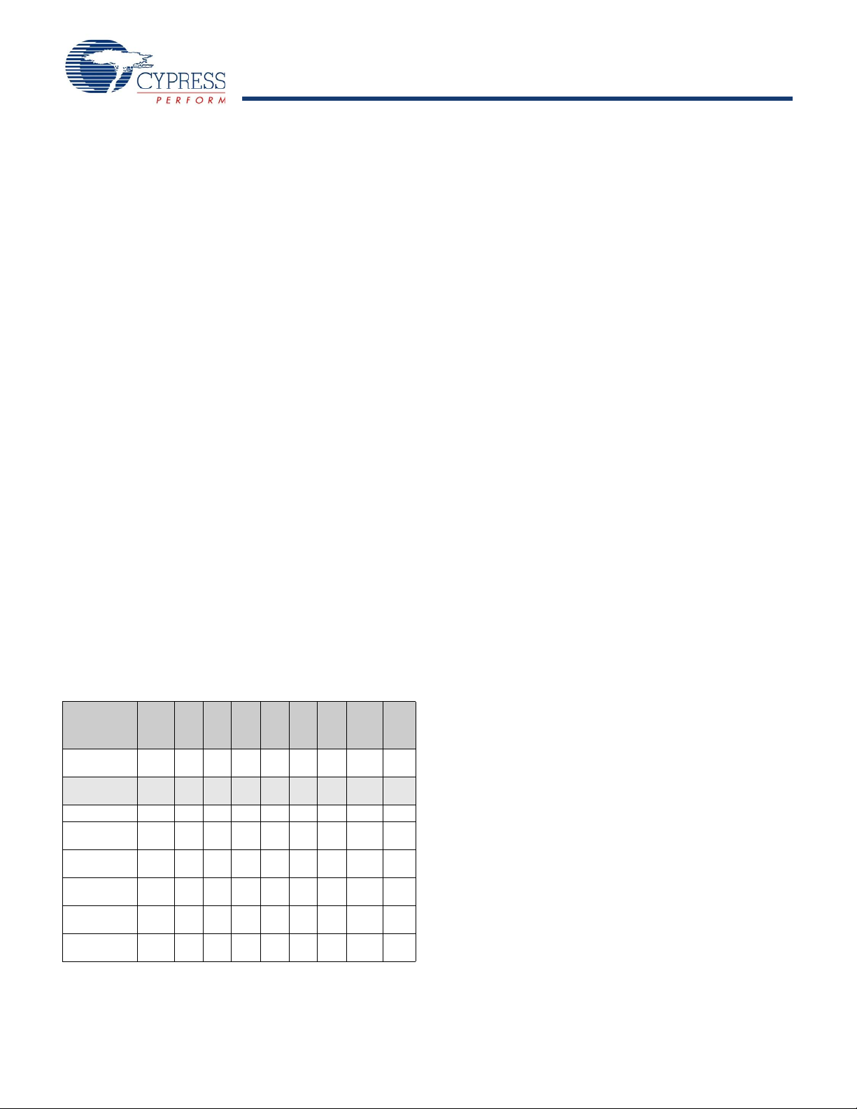
PSoC Device Characteristics
Depending on your PSoC device characteristics, the digital and
analog systems can have 16, 8, or 4 digital blocks and 12, 6, or
4 analog blocks. The following table lists the resources available
for specific PSoC device groups.The PSoC device covered by
this data sheet is highlighted below.
Table 1. PSoC Device Characteristics
PSoC Part
Number
CY8C29x66
CY8C27x43
CY8C24x94 49 1 4 48 2 2 6 1K 16K
CY8C24x23
CY8C24x23A
CY8C21x34
CY8C21x23
CY8C20x34
I/O
Digital
up to
64
up to
44
up to
24
up to
24
up to
28
16 1 4 8 0 2
up to
28
Rows
Digital
4 16 12 4 4 12 2K 32K
2 8 12 4 4 12
1 4 12 2 2 6
1412226
142802
0 0 28 0 0
Inputs
Digital
Blocks
Analog
Analog
Analog
Outputs
Columns
Blocks
Analog
[1]
4
[2]
4
[2]
3
SRAM
256
Bytes
256
Bytes
256
Bytes
512
Bytes
256
Bytes
512
Bytes
Size
Flash
16K
4K
4K
8K
4K
8K
Getting Started
The quickest way to understand PSoC silicon is to read this data
sheet and then use the PSoC Designer Integrated Development
Environment (IDE). This data sheet is an overview of the PSoC
integrated circuit and presents specific pin, register, and
electrical specifications.
For in depth information, along with detailed programming information, see the PSoC
Technical Reference Manual for CY8C28xxx PSoC devices.
For up to date ordering, packaging, and electrical specification
information, see the latest PSoC device data sheets on the web
at www.cypress.com/psoc.
Application Notes
Application notes are an excellent introduction to the wide variety
of possible PSoC designs. They are located here:
www.cypress.com/psoc. Select Application Notes under the
Documentation tab.
Development Kits
PSoC Development Kits are available online from Cypress at
www.cypress.com/shop and through a growing number of
regional and global distributors, which include Arrow, Avnet,
Digi-Key, Farnell, Future Electronics, and Newark.
Training
Free PSoC technical training (on demand, webinars, and
workshops) is available online at www.cypress.com/training. The
training covers a wide variety of topics and skill levels to assist
you in your designs.
CYPros Consultants
Certified PSoC Consultants offer everything from technical
assistance to completed PSoC designs. To contact or become a
PSoC Consultant go to www.cypress.com/cypros.
Solutions Library
Visit our growing library of solution focused designs at
www.cypress.com/solutions. Here you can find various
Size
application designs that include firmware and hardwa re design
files that enable you to complete your designs quickly.
Technical Support
For assistance with technical issues, search KnowledgeBase
articles and forums at www.cypress.com/support. If you cannot
find an answer to your question, call technical support at
1-800-541-4736.
®
Programmable System-on-Chip™
Document Number: 38-12012 Rev. *O Page 5 of 53
[+] Feedback
Page 6

CY8C27143, CY8C27243
CY8C27443, CY8C27543, CY8C27643
Development Tools
PSoC Designer is a Microsoft® Windows-based, integrated
development environment for the Programmable
System-on-Chip (PSoC) devices. The PSoC Designer IDE runs
on Windows XP or Windows Vista.
This system provides design database management by project,
an integrated debugger with In-Circuit Emulator, in-system
programming support, and built in support for third party
assemblers and C compilers.
PSoC Designer also supports C language compilers developed
specifically for the devices in the PSoC family.
PSoC Designer Software Subsystems
System-Level View
A drag-and-drop visual embedded system design environment
based on PSoC Express. In the system level view you create a
model of your system inputs, outputs, and communication
interfaces. You define when and how an output device changes
state based upon any or all other system devices. Based upon
the design, PSoC Designer automatically selects one or more
PSoC Programmable System-on-Chip Controllers that match
your system requirements.
PSoC Designer generates all embedded code, then compiles
and links it into a programming file for a specific PSoC device.
Chip-Level View
The chip-level view is a more traditional IDE. Choose a base
device to work with and then select different onboard analog and
digital components called user modules that use the PSoC
blocks. Examples of user modules are ADCs, DACs, Amplifiers,
and Filters. Configure the user modules for your chosen
application and connect them to each other and to the proper
pins. Then generate your project. This prepopulates your project
with APIs and libraries that you can use to program your
application.
The device editor also supports easy development of multiple
configurations and dynamic reconfiguration. Dynamic
configuration allows for changing configurations at run time.
Hybrid Designs
You can begin in the system-level view, allow it to choose and
configure your user modules, routing, and generate code, then
switch to the chip-level view to gain complete control over
on-chip resources. All views of the project share a common code
editor, builder , and common debug, emulation, and programming
tools.
Code Generation Tools
PSoC Designer supports multiple third party C compilers and
assemblers. The code generation tools work seamlessly within
the PSoC Designer interface and have been tested with a full
range of debugging tools. The choice is yours.
Assemblers. The assemblers allow assembly code to merge
seamlessly with C code. Link libraries automatically use absolute
addressing or are compiled in relative mode, and linked with
other software modules to get absolute addressing.
C Language Compilers. C language compilers are available
that support the PSoC family of devices. The products allow you
to create complete C programs for the PSoC family devices.
The optimizing C compilers provide all the features of C tailored
to the PSoC architecture. They come complete with embedded
libraries providing port and bus operations, standard keypad and
display support, and extended math functionality.
Debugger
The PSoC Designer Debugger subsystem provides hardware
in-circuit emulation, allowing you to test the program in a physical
system while providing an internal view of the PSoC device.
Debugger commands allow the designer to read and program
and read and write data memory, read and write I/O registers,
read and write CPU registers, set and clear b reakpoints, and
provide program run, halt, and step control. The debugger also
allows the designer to create a trace buffer of registers and
memory locations of interest.
Online Help System
The online help system displays online, context-sensitive help
for the user. Designed for procedural and quick reference, each
functional subsystem has its own context-sensitive help. This
system also provides tutorials and links to FAQs and an Online
Support Forum to aid the designer in getting started.
In-Circuit Emulator
A low cost, high functionality In-Circuit Emulator (ICE) is
available for development support. This hardware has the
capability to program single devices.
The emulator consists of a base unit that connects to the PC by
way of a USB port. The base unit is universal and operates with
all PSoC devices. Emulation pods for each device family are
available separately. The emulation pod takes the place of the
PSoC device in the target board and performs full speed (24
MHz) operation.
Document Number: 38-12012 Rev. *O Page 6 of 53
[+] Feedback
Page 7

CY8C27143, CY8C27243
CY8C27443, CY8C27543, CY8C27643
Designing with PSoC Designer
The development process for the PSoC device differs from that
of a traditional fixed function microprocessor. The configurable
analog and digital hardware blocks give the PSoC architecture a
unique flexibility that pays dividends in managing specification
change during development and by lowering inventory costs.
These configurable resources, called PSoC Blocks, have the
ability to implement a wide variety of user selectable functions.
The PSoC development process can be summarized in the
following four steps:
1. Select Components
2. Configure Components
3. Organize and Connect
4. Generate, Verify, and Debug
Select Components
Both the system-level and chip-level views provide a library of
prebuilt, pretested hardware peripheral components. In the
system-level view, these components are called “drivers” and
correspond to inputs (a thermistor, for example), outputs (a
brushless DC fan, for example), communication interfaces
2
(I
C-bus, for example), and the logic to control how they interact
with one another (called valuators).
In the chip-level view, the components are called “user modules”.
User modules make selecting and implementing peripheral
devices simple, and come in analog, digital, and progra mma ble
system-on-chip varieties.
Configure Components
Each of the components you select establishes the basic register
settings that implement the selected function. They also provide
parameters and properties that allow you to tailor their precise
configuration to your particular application. For example, a Pulse
Width Modulator (PWM) User Module configures one or more
digital PSoC blocks, one for each 8 bits of resolution. The user
module parameters permit you to establish the pulse width and
duty cycle. Configure the parameters and properties to
correspond to your chosen application. Enter values directly o r
by selecting values from drop-down menus.
Both the system-level drivers and chip-level user modules are
documented in data sheets that are viewed directly in PSoC
Designer. These data sheets explain the internal operation of the
component and provide performance specifications. Each data
sheet describes the use of each user module parameter or driver
property, and other information you may need to successfully
implement your design.
Organize and Connect
You can build signal chains at the chip level by interconnecting
user modules to each other and the I/O pins, or connect system
level inputs, outputs, and communication interfaces to each
other with valuator functions.
In the system-level view, selecting a potentiometer driver to
control a variable speed fan driver and setting up the valuators
to control the fan speed based on input from the pot selects,
places, routes, and configures a programmable gain amplifier
(PGA) to buffer the input from the potentiometer, an analog to
digital converter (ADC) to convert the potentiometer’s output to
a digital signal, and a PWM to control the fan.
In the chip-level view, perform the selection, configuration, and
routing so that you have complete control over the use of all
on-chip resources.
Generate, Verify, and Debug
When you are ready to test the hardware configuration or move
on to developing code for the project, perform the “Generate
Application” step. This causes PSoC Designer to generate
source code that automatically configures the device to your
specification and provides the software for the system.
Both system-level and chip-level designs generate software
based on your design. The chip-level design provides application
programming interfaces (APIs) with high level functions to
control and respond to hardware events at run time and interrupt
service routines that you can adapt as needed. The system-level
design also generates a C main() program that completely
controls the chosen application and contains placeholders for
custom code at strategic positions allowing you to further refine
the software without disrupting the generated code.
A complete code development environment allows you to
develop and customize your applications in C, assembly
language, or both.
The last step in the development process takes place inside
PSoC Designer’s Debugger subsystem. The Debugger
downloads the HEX image to the ICE where it runs at full speed.
Debugger capabilities rival those of systems costing many times
more. In addition to traditional single-step, run-to-breakpoint and
watch-variable features, the Debugger provides a large trace
buffer and allows you define complex breakpoint events that
include monitoring address and data bus values, memory
locations and external signals.
Document Number: 38-12012 Rev. *O Page 7 of 53
[+] Feedback
Page 8
CY8C27143, CY8C27243
CY8C27443, CY8C27543, CY8C27643
Document Conventions
Acronyms Used
This table lists the acronyms used in this data sheet.
Table 2. Acronyms
Acronym Description
AC alternating current
ADC analog-to-digital converter
API application programming interface
CPU central processing unit
CT continuous time
DAC digital-to-analog converter
DC direct current
EEPROM electrically erasable programmable read-only
FSR full scale range
GPIO general purpose I/O
ICE in-circuit emulator
IDE integrated development environment
I/O input/output
ISSP in-system serial programming
IPOR imprecise power on reset
LSb least-significant bit
LVD low voltage detect
MSb most-significant bit
PC program counter
PGA programmable gain amplifier
POR power on reset
PPOR precision power on reset
®
PSoC
PWM pulse width modulator
ROM read only memory
SC switched capacitor
SMP switch mode pump
SRAM static random access memory
memory
Programmable System-on-Chip™
Units of Measure
A units of measure table is located in the section
Electrical S pecificat ions on page 19. Table 13 on page 19 lists all
the abbreviations used to measure the PSoC devices.
Numeric Naming
Hexadecimal numbers are represented with all letters in
uppercase with an appended lowercase ‘h’ (for example, ‘14h’ or
‘3Ah’). Hexadecimal numbers may also be represented by a ‘0x’
prefix, the C coding convention. Binary numbers have an
appended lowercase ‘b’ (for example, 01010100b’ or
‘01000011b’). Numbers not indicated by an ‘h’, ‘b’, or 0x are
decimal.
Document Number: 38-12012 Rev. *O Page 8 of 53
[+] Feedback
Page 9
CY8C27143, CY8C27243
CY8C27443, CY8C27543, CY8C27643
Pinouts
PDIP
1
2
3
4
A, IO, P 0[5]
A, IO, P 0[3]
I2C S CL, XTALin, P1[1]
Vss
8
7
6
5
Vdd
P0[4], A, IO
P0[2], A, IO
P1[0], XTALout, I2C SDA
SSOP
SOIC
Vdd
P0[6], A, I
P0[4], A, IO
P0[2], A, IO
P0[0], A, I
XRES
P1[6]
P1[4], EXTCLK
P1[2]
P1[0], XTALout, I2C SDA
20
19
18
17
16
15
14
13
12
11
1
2
3
4
5
6
7
8
9
10
A, I, P0[7]
A, IO, P0[5]
A, IO, P0[3]
A, I, P 0[1]
SMP
I2C SCL, P1[7]
I2C SDA, P1[5]
P1[3]
I2C SCL, XTALin, P1[1]
Vss
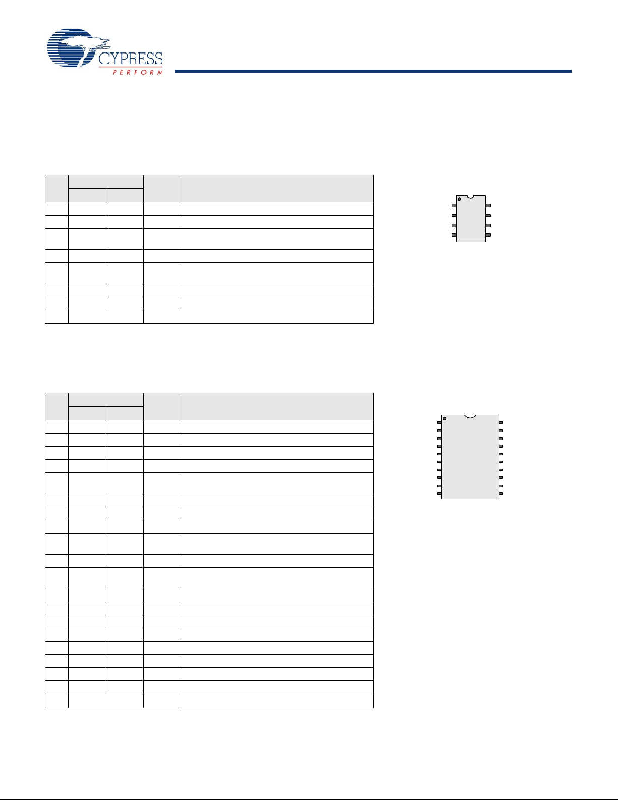
The CY8C27x43 PSoC device is available in a variety of packages which are listed and illustrated in the following tables. Every port
pin (labeled with a “P”) is capable of Digital I/O. However, Vss, Vdd, SMP, and XRES are not capable of Digital I/O.
8-Pin Part Pinout
Table 3. Pin Definitions - 8-Pin PDIP
Pin
No.
LEGEND: A = Analog, I = Input, and O = Output.
* These are the ISSP pins, which are not High Z at POR (Power On Reset). See the PSoC Programmable System-on-Chip Technical Reference
Manual for details.
20-Pin Part Pinout
Table 4. Pin Definitions - 20-Pin SSOP, SOIC
Pin
No.
10 Power Vss Ground connection.
12 I/O P1[2]
13 I/O P1[4] Optional External Clock Input (EXTCLK).
14 I/O P1[6]
15 Input XRES Active high external reset with internal pull down.
16 I/O I P0[0] Analog column mux input.
17 I/O I/O P0[2] Analog column mux input and column output.
18 I/O I/O P0[4] Analog column mux input and column output.
19 I/O I P0[6] Analog column mux input.
20 Power Vdd Supply voltage.
LEGEND: A = Analog, I = Input, and O = Output.
* These are the ISSP pins, which are not High Z at POR (Power On Reset). See the PSoC Programmable System-on-Chip Technical Reference Manual for details.
Document Number: 38-12012 Rev. *O Page 9 of 53
Type
Digital Analog
Pin
Name
Description
1 I/O I/O P0[5] Analog column mux input and column output.
2 I/O I/O P0[3] Analog column mux input and column output.
3 I/O P1[1] Crystal Input (XTALin), I2C Serial Clock (SCL),
ISSP-SCLK*.
4 Power Vss Ground connection.
5 I/O P1[0] Crystal Output (XTALout), I2C Serial Data (SDA),
ISSP-SDATA*.
6 I/O I/O P0[2] Analog column mux input and column output.
7 I/O I/O P0[4] Analog column mux input and column output.
8 Power Vdd Supply voltage.
Type
Digital Analog
Pin
Name
Description
1 I/O I P0[7] Analog column mux input.
2 I/O I/O P0[5] Analog column mux input and column output.
3 I/O I/O P0[3] Analog column mux input and column output.
4 I/O I P0[1] Analog column mux input.
5 Power SMP Switch Mode Pump (SMP) connection to external
components required.
6 I/O P1[7] I2C Serial Clock (SCL).
7 I/O P1[5] I2C Serial Data (SDA).
8 I/O P1[3]
9 I/O P1[1] Crystal Input (XTALin), I2C Serial Clock (SCL),
ISSP-SCLK*.
11 I/O P1[0] Crystal Output (XTALout), I2C Serial Data (SDA),
ISSP-SDATA*.
Figure 3. CY8C27143 8-Pin PSoC Device
Figure 4. CY8C27243 20-Pin PSoC Device
[+] Feedback
Page 10
CY8C27143, CY8C27243
CY8C27443, CY8C27543, CY8C27643
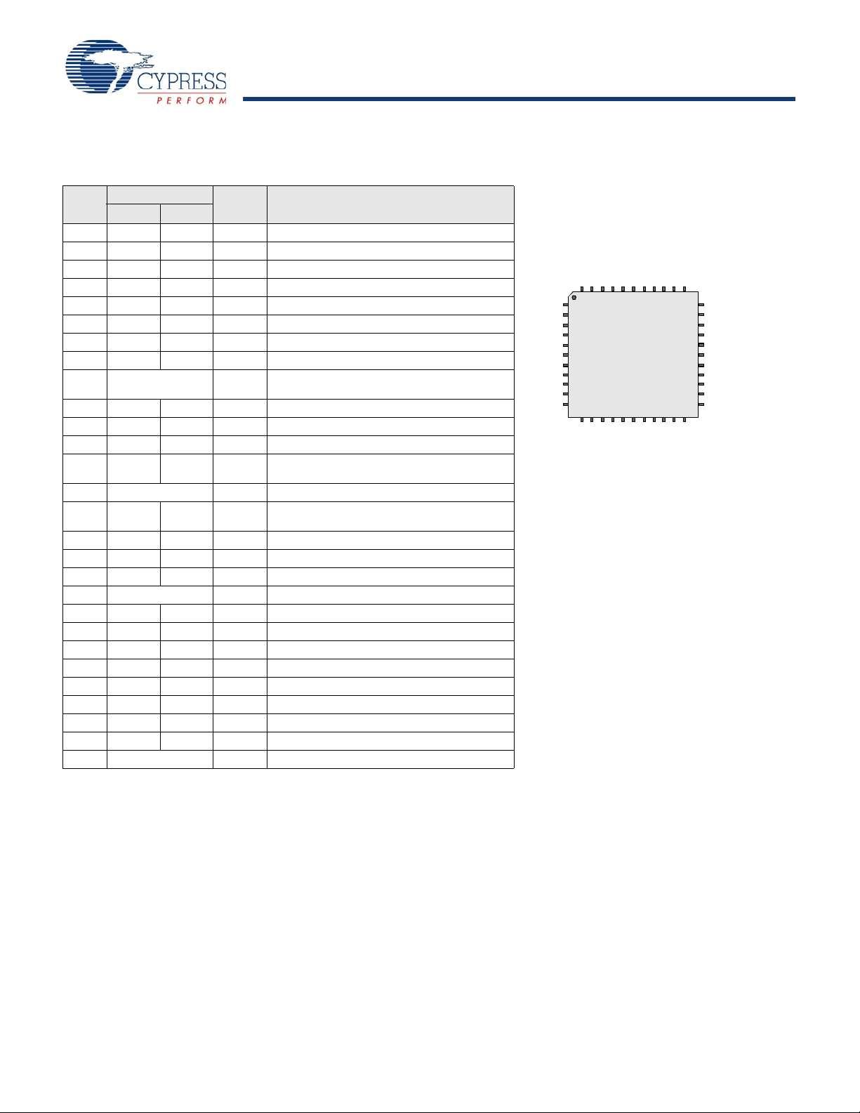
28-Pin Part Pinout
A, I, P0[7]
A, IO, P 0[5]
A, IO, P 0[3]
A, I, P0[1]
P2[7]
P2[5]
A, I, P2[3]
A, I, P2[1]
SMP
I2C SCL, P1[7]
I2C SDA, P1[5]
P1[3]
I2C SCL, XTALin, P1[1]
Vss
Vdd
P0[6], A, I
P0[4], A, IO
P0[2], A, IO
P0[0], A, I
P2[6], External VRef
P2[4], External AGND
P2[2], A, I
P2[0], A, I
XRES
P1[6]
P1[4], EXTCLK
P1[2]
P1[0], XTALout, I2C SDA
PDIP
SSOP
SOIC
1
2
3
4
5
6
7
8
9
10
11
12
13
14
28
27
26
25
24
23
22
21
20
19
18
17
16
15
TQFP
P3[1]
P2[7]
P2[5] P2[4], External AGND
A, I, P2[3] P2[2], A, I
A, I, P2[1] P2[0], A, I
P4[7]
P4[6]
P4[5]
P4[4]
P4[3]
P4[2]
P4[1]
P4[0]
SMP XRES
P3[7]
P3[6]
P3[5] P3[4]
P3[3] P3[2]
I2C SC L, P1[7]
P0[1], A, I
I2C SDA, P1[5]
P0[3], A, IO
P1[3]
P0[5], A, IO
I2C SCL, XTALin, P1[1]
P0[7], A, I
Vss
Vdd
I2C SDA, XTALout, P1[0 ]
P0[6], A, I
P1[2]
P0[4], A, IO
EXTCLK, P1[4]
P0[2], A, IO
P1[6]
P0[0], A, I
P3[0]
P2[6], External VRef
33
32
31
30
29
28
27
26
25
24
23
1
2
3
4
5
6
7
8
9
10
11
4443424140393837363534
13
14
15
16
17
18
192021
22
12
Table 5. Pin Definitions - 28-Pin PDIP, SSOP, SOIC
Pin No.
Type
Digital Analog
1 I/O I P0[7] Analog column mux input.
2 I/O I/O P0[5] Analog column mux input and column output.
3 I/O I/O P0[3] Analog column mux input and column output.
4 I/O I P0[1] Analog column mux input.
5 I/O P2[7]
6 I/O P2[5]
7 I/O I P2[3] Direct switched capacitor block input.
8 I/O I P2[1] Direct switched capacitor block input.
9 Power SMP Switch Mode Pump (SMP) connection to external
10 I/O P1[7] I2C Serial Clock (SCL).
11 I/O P1[5] I2C Serial Data (SDA).
12 I/O P1[3]
13 I/O P1[1] Crystal Input (XTALin), I2C Serial Clock (SCL),
14 Power Vss Ground connection.
15 I/O P1[0] Crystal Output (XT ALout), I2C Serial Data (SDA),
16 I/O P1[2]
17 I/O P1[4] Optional External Clock Input (EXTCLK).
18 I/O P1[6]
19 Input XRES Active high external reset with internal pull down.
20 I/O I P2[0] Direct switched capacitor block input.
21 I/O I P2[2] Direct switched capacitor block input.
22 I/O P2[4] External Analog Ground (AGND).
23 I/O P2[6] External Voltage Reference (VRef).
24 I/O I P0[0] Analog column mux input.
25 I/O I/O P0[2] Analog column mux input and column output.
26 I/O I/O P0[4] Analog column mux input and column output.
27 I/O I P0[6] Analog column mux input.
28 Power Vdd Supply voltage.
Pin
Name
Description
components required.
ISSP-SCLK*.
ISSP-SDATA*.
Figure 5. CY8C27443 28-Pin PSoC Device
LEGEND: A = Analog, I = Input, and O = Output.
* These are the ISSP pins, which are not High Z at POR (Power On Reset). See the PSo C Programmable System-on-Chip Technical Reference Manual for details.
Document Number: 38-12012 Rev. *O Page 10 of 53
[+] Feedback
Page 11
CY8C27143, CY8C27243
CY8C27443, CY8C27543, CY8C27643
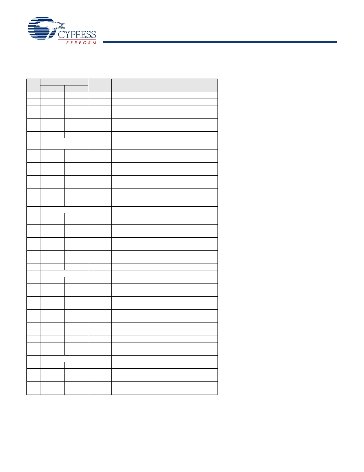
44-Pin Part Pinout
Table 6. Pin Definitions - 44-Pin TQFP
Pin
No.
1 I/O P2[5]
2 I/O I P2[3] Direct switched capacitor block input.
3 I/O I P2[1] Direct switched capacitor block input.
4 I/O P4[7]
5 I/O P4[5]
6 I/O P4[3]
7 I/O P4[1]
8 Power SMP Switch Mode Pump (SMP) connection to external
9 I/O P3[7]
10 I/O P3[5]
11 I/O P3[3]
12 I/O P3[1]
13 I/O P1[7] I2C Serial Clock (SCL).
14 I/O P1[5] I2C Serial Data (SDA).
15 I/O P1[3]
16 I/O P1[1] Crystal Input (XTALin), I2C Serial Clock (SCL),
17 Power Vss Ground connection.
18 I/O P1[0] Crystal Output (XT ALout), I2C Serial Data (SDA),
19 I/O P1[2]
20 I/O P1[4] Optional External Clock Input (EXTCLK).
21 I/O P1[6]
22 I/O P3[0]
23 I/O P3[2]
24 I/O P3[4]
25 I/O P3[6]
26 Input XRES Active high external reset with internal pull down.
27 I/O P4[0]
28 I/O P4[2]
29 I/O P4[4]
30 I/O P4[6]
31 I/O I P2[0] Direct switched capacitor block input.
32 I/O I P2[2] Direct switched capacitor block input.
33 I/O P2[4] External Analog Ground (AGND).
34 I/O P2[6] External Voltage Reference (VRef).
35 I/O I P0[0] Analog column mux input.
36 I/O I/O P0[2] Analog column mux input and column output.
37 I/O I/O P0[4] Analog column mux input and column output.
38 I/O I P0[6] Analog column mux input.
39 Power Vdd Supply voltage.
40 I/O I P0[7] Analog column mux input.
41 I/O I/O P0[5] Analog column mux input and column output.
42 I/O I/O P0[3] Analog column mux input and column output.
43 I/O I P0[1] Analog column mux input.
44 I/O P2[7]
Type
Digital Analog
Pin Name Description
components required.
ISSP-SCLK*.
ISSP-SDATA*.
Figure 6. CY8C27543 44-Pin PSoC Device
LEGEND: A = Analog, I = Input, and O = Output.
* These are the ISSP pins, which are not High Z at POR (Power On Reset). See the PSoC Programmable System-on-Chip Technical Reference Manual for details.
Document Number: 38-12012 Rev. *O Page 11 of 53
[+] Feedback
Page 12
CY8C27143, CY8C27243
CY8C27443, CY8C27543, CY8C27643
48-Pin Part Pinout
SSOP
A, I, P0[7]
Vdd
A, IO, P0[5]
P0[6], A, I
A, IO, P0[3]
P0[4], A, IO
A, I, P0[1] P0[2], A, IO
P2[7]
P0[0], A, I
P2[5]
P2[6], External VRef
A, I, P2[3]
P2[4], External AGND
A, I, P2[1]
P2[2], A, I
P4[7]
P2[0], A, I
P4[5]
P4[6]
P4[3]
P4[4]
P4[1]
P4[2]
SMP
P4[0]
P3[7]
XRES
P3[5]
P3[6]
P3[3]
P3[4]
P3[1]
P3[2]
P5[3]
P3[0]
P5[1]
P5[2]
I2C SCL, P1[7]
P5[0]
I2C SDA, P1[5]
P1[6]
P1[3]
P1[4], EXT CLK
I2C SCL, XTALin, P1[1] P1[2]
Vss P1[0], XTALout, I2C SDA
1
2
3
4
5
6
7
8
9
10
11
12
13
14
15
16
17
18
19
20
21
22
23
24
48
47
46
45
43
44
42
40
41
39
38
37
36
35
33
34
32
31
30
29
28
27
26
25
Table 7. 48-Pin Part Pinout (SSOP)
Pin
No.
1 I/O I P0[7] Analog column mux input.
2 I/O I/O P0[5] Analog column mux input and column output.
3 I/O I/O P0[3] Analog column mux input and column output.
4 I/O I P0[1] Analog column mux input.
5 I/O P2[7]
6 I/O P2[5]
7 I/O I P2[3] Direct switched capacitor block input.
8 I/O I P2[1] Direct switched capacitor block input.
9 I/O P4[7]
10 I/O P4[5]
11 I/O P4[3]
12 I/O P4[1]
13 Power SMP Switch Mode Pump (SMP) connection to
14 I/O P3[7]
15 I/O P3[5]
16 I/O P3[3]
17 I/O P3[1]
18 I/O P5[3]
19 I/O P5[1]
20 I/O P1[7] I2C Serial Clock (SCL).
21 I/O P1[5] I2C Serial Data (SDA).
22 I/O P1[3]
23 I/O P1[1] Crystal Input (XTALin), I2C Serial Clock
24 Power Vss Ground connection.
25 I/O P1[0] Crystal Output (XTALout), I2C Serial Data
26 I/O P1[2]
27 I/O P1[4] Optional External Clock Input (EXTCLK).
28 I/O P1[6]
29 I/O P5[0]
30 I/O P5[2]
31 I/O P3[0]
32 I/O P3[2]
33 I/O P3[4]
34 I/O P3[6]
35 Input XRES Active high external reset with internal pull
36 I/O P4[0]
37 I/O P4[2]
38 I/O P4[4]
39 I/O P4[6]
40 I/O I P2[0] Direct switched capacitor block input.
41 I/O I P2[2] Direct switched capacitor block input.
42 I/O P2[4] External Analog Ground (AGND).
43 I/O P2[6] External Voltage Reference (VRef).
44 I/O I P0[0] Analog column mux input.
45 I/O I/O P0[2] Analog column mux input and column output.
46 I/O I/O P0[4] Analog column mux input and column output.
47 I/O I P0[6] Analog column mux input.
48 Power Vdd Supply voltage.
LEGEND: A = Analog, I = Input, and O = Output.
* These are the ISSP pins, which are not High Z at POR (Power On Reset). See the PSoC Mixed-Signal Array Technical Reference Manual for details.
Document Number: 38-12012 Rev. *O Page 12 of 53
Type
Digital Analog
Pin
Name
external components required.
(SCL), ISSP-SCLK*.
(SDA), ISSP-SDATA.*
down.
Description
Figure 7. CY8C27643 48-Pin PSoC Device
[+] Feedback
Page 13
CY8C27143, CY8C27243
CY8C27443, CY8C27543, CY8C27643
QFN
(Top View)
P2[5]
P2[7]
P0[1], A, I
P0[3], A, IO
P0[5], A, IO
P0[7], A, I
Vdd
P0[6], A, I
P0[4], A, IO
P0[2], A, IO
P0[0], A, I
P2[6], External VRef
10
11
12
A, I, P2[3]
A, I, P2[1]
P4[7]
P4[5]
P4[3]
P4[1]
SMP
P3[7]
P3[5]
P3[3]
P3[1]
P5[3]
35
34
33
32
31
30
29
28
27
26
25
36
4847464544
43424140393837
P2[2], A, I
P2[0], A, I
P4[6]
P4[4]
P4[2]
P4[0]
XRES
P3[6]
P3[4]
P3[2]
P3[0]
P2[4], External AGND
1
2
3
4
5
6
7
8
9
1314151617181920212223
24
P5[1]
I2C SCL, P1[7]
I2C SDA, P1[5]
P1[3]
I2C SCL, XTALin, P1[1]
Vss
I2C SDA, XTALout, P1[0]
P1[2]
EXTCLK, P1[4]
P1[6]
P5[0]
P5[2]
Table 8. 48-Pin Part Pinout (QFN)*
Pin
No.
1 I/O I P2[3] Direct switched capacitor block input.
2 I/O I P2[1] Direct switched capacitor block input.
3 I/O P4[7]
4 I/O P4[5]
5 I/O P4[3]
6 I/O P4[1]
7 Power SMP Switch Mode Pump (SMP) connection to
8 I/O P3[7]
9 I/O P3[5]
10 I/O P3[3]
11 I/O P3[1]
12 I/O P5[3]
13 I/O P5[1]
14 I/O P1[7] I2C Serial Clock (SCL).
15 I/O P1[5] I2C Serial Data (SDA).
16 I/O P1[3]
17 I/O P1[1] Crystal Input (XTALin), I2C Serial Clock (SCL),
18 Power Vss Ground connection.
19 I/O P1[0] Crystal Output (XTALout), I2C Serial Data
20 I/O P1[2]
21 I/O P1[4] Optional External Clock Input (EXTCLK).
22 I/O P1[6]
23 I/O P5[0]
24 I/O P5[2]
25 I/O P3[0]
26 I/O P3[2]
27 I/O P3[4]
28 I/O P3[6]
29 Input XRES Active high external reset with internal pull
30 I/O P4[0]
31 I/O P4[2]
32 I/O P4[4]
33 I/O P4[6]
34 I/O I P2[0] Direct switched capacitor block input.
35 I/O I P2[2] Direct switched capacitor block input.
36 I/O P2[4] External Analog Ground (AGND).
37 I/O P2[6] External Voltage Reference (VRef).
38 I/O I P0[0] Analog column mux input.
39 I/O I/O P0[2] Analog column mux input and column output.
40 I/O I/O P0[4] Analog column mux input and column output.
41 I/O I P0[6] Analog column mux input.
42 Power Vdd Supply voltage.
43 I/O I P0[7] Analog column mux input.
44 I/O I/O P0[5] Analog column mux input and column output.
45 I/O I/O P0[3] Analog column mux input and column output.
46 I/O I P0[1] Analog column mux input.
47 I/O P2[7]
48 I/O P2[5]
LEGEND: A = Analog, I = Input, and O = Output.
* The QFN package has a center pad that must be connected to ground (Vss).
** These are the ISSP pins, which are not High Z at POR (Power On Reset). See the PSoC Mixed-Signal Array Technical Reference Manual for details.
Type
Digital Analog
Pin
Name
Description
external components required.
ISSP-SCLK**.
(SDA), ISSP-SDATA**.
down.
Figure 8. CY8C27643 48-Pin PSoC Device
Document Number: 38-12012 Rev. *O Page 13 of 53
[+] Feedback
Page 14
CY8C27143, CY8C27243
CY8C27443, CY8C27543, CY8C27643
56-Pin Part Pinout
SSOP
1
56
255
354
453
5
52
6
51
750
849
948
10
47
11 46
12 45
13
44
14 43
15
42
16
41
17
40
18 39
19 38
20
37
21 36
22
35
23 34
24 33
25 32
26 31
27
30
28
29
Vdd
P0[6], AI
P0[4], AIO
P0[2], AIO
P0[0], AI
P2[6], Externa l V R e f
P2[4], Externa l A GND
P2[2], AI
P2[0], AI
P4[6]
P4[4]
P4[2]
P4[0]
CCLK
HCLK
XRES
P3[6]
P3[4]
P3[2]
P3[0]
P5[2]
P5[0]
P1[6]
P1[4], EXTCLK
P1[2]
P1[0], XTALOut, I2C SDA, SDATA
NC
NC
AI, P0[7]
AIO, P0[5]
AIO, P0[3]
AI, P0[1]
P2[7]
P2[5]
AI, P2[3]
AI, P2[1]
P4[7]
P4[5]
P4[3]
P4[1]
OCDE
OCDO
SMP
P3[7]
P3[5]
P3[3]
P3[1]
P5[3]
P5[1]
I2C SCL, P1[7]
I2C SDA, P1[5]
NC
P1[3]
SCLK, I2C SCL, XTALIn, P1[1]
Vss
NC
The 56-pin SSOP part is for the CY8C27002 On-Chip Debug (OCD) PSoC device.
Note This part is only used for in-circuit debugging. It is NOT available for production.
Table 9. 56-Pin Part Pinout (SSOP)
Pin
No.
Type
Digital Analog
Pin
Name
Description
1 NC No connection.
2 I/O I P0[7] Analog column mux input.
3 I/O I P0[5] Analog column mux input and column
output.
4 I/O I P0[3] Analog column mux input and column
output.
5 I/O I P0[1] Analog column mux input.
6 I/O P2[7]
7 I/O P2[5]
8 I/O I P2[3] Direct switched capacitor block input.
9 I/O I P2[1] Direct switched capacitor block input.
10 I/O P4[7]
11 I/O P4[5]
12 I/O IP4[3]
13 I/O IP4[1]
14 OCD OCDE OCD even data I/O.
15 OCD OCDO OCD odd data output.
16 Power SMP Switch Mode Pump (SMP) connection to
required external components.
17 I/O P3[7]
18 I/O P3[5]
19 I/O P3[3]
20 I/O P3[1]
21 I/O P5[3]
22 I/O P5[1]
23 I/O P1[7] I2C Serial Clock (SCL).
24 I/O P1[5] I2C Serial Data (SDA).
25 NC No connection.
26 I/O P1[3]
27 I/O P1[1] Crystal Input (XTALin), I2C Serial Clock
(SCL), ISSP-SCLK*.
28 Power Vdd Supply voltage.
29 NC No connection.
30 NC No connection..
31 I/O P1[0] Crystal Output (XTALout), I2C Serial
32 I/O P1[2]
33 I/O P1[4] Optional External Clock Input (EXTCLK).
34 I/O P1[6]
35 I/O P5[0]
36 I/O P5[2]
37 I/O P3[0]
38 I/O P3[2]
39 I/O P3[4]
40 I/O P3[6]
41 Input XRES Active high external reset with internal
Document Number: 38-12012 Rev. *O Page 14 of 53
Data (SDA), ISSP-SDATA*.
pull down.
Figure 9. CY8C27002 56-Pin PSoC Device
Not for Production
[+] Feedback
Page 15
CY8C27143, CY8C27243
CY8C27443, CY8C27543, CY8C27643
Table 9. 56-Pin Part Pinout (SSOP)
42 OCD HCLK OCD high-speed clock output.
43 OCD CCLK OCD CPU clock output.
44 I/O P4[0]
45 I/O P4[2]
46 I/O P4[4]
47 I/O P4[6]
48 I/O I P2[0] Direct switched capacitor block input.
49 I/O I P2[2] Direct switched capacitor block input.
50 I/O P2[4] External Analog Ground (AGND).
51 I/O P2[6] External Voltage Reference (VRef).
52 I/O I P0[0] Analog column mux input.
53 I/O I P0[2] Analog column mux input and column
54 I/O I P0[4] Analog column mux input and column
55 I/O I P0[6] Analog column mux input.
56 Power Vdd Supply voltage.
output.
output.
LEGEND
* These are the ISSP pins, which are not High Z at POR (Power On Reset). See the PSoC Mixed-Signal Array Technical Reference Manual for details.
: A = Analog, I = Input, O = Output, and OCD = On-Chip Debug.
Document Number: 38-12012 Rev. *O Page 15 of 53
[+] Feedback
Page 16
CY8C27143, CY8C27243
CY8C27443, CY8C27543, CY8C27643
Register Reference
This chapter lists the registers of the CY8C27x43 PSoC device.
For detailed register information, reference the
PSoC Programmable System-on-Chip Technical Reference
Manual.
Register Conventions
The register conventions specific to this section are listed in the
Register Mapping Tables
The PSoC device has a total register address space of 512
bytes. The register space is referred to as I/O space and is
divided into two banks. The XOI bit in the Flag register (CPU_F)
determines which bank the user is currently in. When the XOI bit
is set the user is in Bank 1.
Note In the following register mapping tables, blank fields are
reserved and must not be accessed.
following table.
Table 10. Register Conventions
Convention Description
R Read register or bit(s)
W Write register or bit(s)
L Logical register or bit(s)
C Clearable register or bit(s)
# Access is bit specific
Table 11. Register Map Bank 0 Table: User Space
Name
PRT0DR 00 RW 40 ASC10CR0 80 RW C0
PRT0IE 01 RW 41 ASC10CR1 81 RW C1
PRT0GS 02 RW 42 ASC10CR2 82 RW C2
PRT0DM2 03 RW 43 ASC10CR3 83 RW C3
PRT1DR 04 RW 44 ASD11CR0 84 RW C4
PRT1IE 05 RW 45 ASD11CR1 85 RW C5
PRT1GS 06 RW 46 ASD11CR2 86 RW C6
PRT1DM2 07 RW 47 ASD11CR3 87 RW C7
PRT2DR 08 RW 48 ASC12CR0 88 RW C8
PRT2IE 09 RW 49 ASC12CR1 89 RW C9
PRT2GS 0A RW 4A ASC12CR2 8A RW CA
PRT2DM2 0B RW 4B ASC12CR3 8B RW CB
PRT3DR 0C RW 4C ASD13CR0 8C RW CC
PRT3IE 0D RW 4D ASD13CR1 8D RW CD
PRT3GS 0E RW 4E ASD13CR2 8E RW CE
PRT3DM2 0F RW 4F ASD13CR3 8F RW CF
PRT4DR 10 RW 50 ASD20CR0 90 RW D0
PRT4IE 11 RW 51 ASD20CR1 91 RW D1
PRT4GS 12 RW 52 ASD20CR2 92 RW D2
PRT4DM2 13 RW 53 ASD20CR3 93 RW D3
PRT5DR 14 RW 54 ASC21CR0 94 RW D4
PRT5IE 15 RW 55 ASC21CR1 95 RW D5
PRT5GS 16 RW 56 ASC21CR2 96 RW I2C_CFG D6 RW
PRT5DM2 17 RW 57 ASC21CR3 97 RW I2C_SCR D7 #
DBB00DR0 20 # AMX_IN 60 RW A0 INT_MSK0 E0 RW
DBB00DR1 21 W 61 A1 INT_MSK1 E1 RW
DBB00DR2 22 RW 62 A2 INT_VC E2 RC
DBB00CR0 23 # ARF_CR 63 RW A3 RES_WDT E3 W
DBB01DR0 24 # CMP_CR0 64 # A4 DEC_DH E4 RC
DBB01DR1 25 W ASY_CR 65 # A5 DEC_DL E5 RC
Blank fields are Reserved and must not be accessed. # Access is bit specific.
(0,Hex)
Addr
18 58 ASD22CR0 98 RW I2C_DR D8 RW
19 59 ASD22CR1 99 RW I2C_MSCR D9 #
1A 5A ASD22CR2 9A RW INT_CLR0 DA RW
1B 5B ASD22CR3 9B RW INT_CLR1 DB RW
1C 5C ASC23CR0 9C RW DC
1D 5D ASC23CR1 9D RW INT_CLR3 DD RW
1E 5E ASC23CR2 9E RW INT_MSK3 DE RW
1F 5F ASC23CR3 9F RW DF
Access
Name
(0,Hex)
Access
Addr
Name
(0,Hex)
Access
Addr
Name
(0,Hex)
Addr
Access
Document Number: 38-12012 Rev. *O Page 16 of 53
[+] Feedback
Page 17

CY8C27143, CY8C27243
CY8C27443, CY8C27543, CY8C27643
Table 11. Register Map Bank 0 Table: User Space (continued)
Name
DBB01DR2 26 RW CMP_CR1 66 RW A6 DEC_CR0 E6 RW
DBB01CR0 27 # 67 A7 DEC_CR1 E7 RW
DCB02DR0 28 # 68 A8 MUL_X E8 W
DCB02DR1 29 W 69 A9 MUL_Y E9 W
DCB02DR2 2A RW 6A AA MUL_DH EA R
DCB02CR0 2B # 6B AB MUL_DL EB R
DCB03DR0 2C # 6C AC ACC_DR1 EC RW
DCB03DR1 2D W 6D AD ACC_DR0 ED RW
DCB03DR2 2E RW 6E AE ACC_DR3 EE RW
DCB03CR0 2F # 6F AF ACC_DR2 EF RW
DBB10DR0 30 # ACB00CR3 70 RW RDI0RI B0 RW F0
DBB10DR1 31 W ACB00CR0 71 RW RDI0SYN B1 RW F1
DBB10DR2 32 RW ACB00CR1 72 RW RDI0IS B2 RW F2
DBB10CR0 33 # ACB00CR2 73 RW RDI0LT0 B3 RW F3
DBB11DR0 34 # ACB01CR3 74 RW RDI0LT1 B4 RW F4
DBB11DR1 35 W ACB01CR0 75 RW RDI0RO0 B5 RW F5
DBB11DR2 36 RW ACB01CR1 76 RW RDI0RO1 B6 RW F6
DBB11CR0 37 # ACB01CR2 77 RW B7 CPU_F F7 RL
DCB12DR0 38 # ACB02CR3 78 RW RDI1RI B8 RW F8
DCB12DR1 39 W ACB02CR0 79 RW RDI1SYN B9 RW F9
DCB12DR2 3A RW ACB02CR1 7A RW RDI1IS BA RW FA
DCB12CR0 3B # ACB02CR2 7B RW RDI1LT0 BB RW FB
DCB13DR0 3C # ACB03CR3 7C RW RDI1LT1 BC RW FC
DCB13DR1 3D W ACB03CR0 7D RW RDI1RO0 BD RW FD
DCB13DR2 3E RW ACB03CR1 7E RW RDI1RO1 BE RW CPU_SCR1 FE #
DCB13CR0 3F # ACB03CR2 7F RW BF CPU_SCR0 FF #
Blank fields are Reserved and must not be accessed. # Access is bit specific.
(0,Hex)
Addr
Access
Name
(0,Hex)
Addr
Access
Name
(0,Hex)
Addr
Access
Name
(0,Hex)
Addr
Table 12. Register Map Bank 1 Table: Configuration Space
Name
(1,Hex)
Addr
Access
Name
(1,Hex)
Access
Addr
Name
(1,Hex)
Access
Addr
Name
(1,Hex)
Addr
Access
Access
PRT0DM0 00 RW 40 ASC10CR0 80 RW C0
PRT0DM1 01 RW 41 ASC10CR1 81 RW C1
PRT0IC0 02 RW 42 ASC10CR2 82 RW C2
PRT0IC1 03 RW 43 ASC10CR3 83 RW C3
PRT1DM0 04 RW 44 ASD11CR0 84 RW C4
PRT1DM1 05 RW 45 ASD11CR1 85 RW C5
PRT1IC0 06 RW 46 ASD11CR2 86 RW C6
PRT1IC1 07 RW 47 ASD11CR3 87 RW C7
PRT2DM0 08 RW 48 ASC12CR0 88 RW C8
PRT2DM1 09 RW 49 ASC12CR1 89 RW C9
PRT2IC0 0A RW 4A ASC12CR2 8A RW CA
PRT2IC1 0B RW 4B ASC12CR3 8B RW CB
PRT3DM0 0C RW 4C ASD13CR0 8C RW CC
PRT3DM1 0D RW 4D ASD13CR1 8D RW CD
PRT3IC0 0E RW 4E ASD13CR2 8E RW CE
PRT3IC1 0F RW 4F ASD13CR3 8F RW CF
PRT4DM0 10 RW 50 ASD20CR0 90 RW GDI_O_IN D0 RW
PRT4DM1 11 RW 51 ASD20CR1 91 RW GDI_E_IN D1 RW
PRT4IC0 12 RW 52 ASD20CR2 92 RW GDI_O_OU D2 RW
PRT4IC1 13 RW 53 ASD20CR3 93 RW GDI_E_OU D3 RW
PRT5DM0 14 RW 54 ASC21CR0 94 RW D4
PRT5DM1 15 RW 55 ASC21CR1 95 RW D5
PRT5IC0 16 RW 56 ASC21CR2 96 RW D6
PRT5IC1 17 RW 57 ASC21CR3 97 RW D7
Blank fields are Reserved and must not be accessed. # Access is bit specific.
Document Number: 38-12012 Rev. *O Page 17 of 53
18 58 ASD22CR0 98 RW D8
19 59 ASD22CR1 99 RW D9
1A 5A ASD22CR2 9A RW DA
1B 5B ASD22CR3 9B RW DB
[+] Feedback
Page 18
CY8C27143, CY8C27243
CY8C27443, CY8C27543, CY8C27643
Table 12. Register Map Bank 1 Table: Configuration Space (continued)
Name
DBB00FN 20 RW CLK_CR0 60 RW A0 OSC_CR0 E0 RW
DBB00IN 21 RW CLK_CR1 61 RW A1 OSC_CR1 E1 RW
DBB00OU 22 RW ABF_CR0 62 RW A2 OSC_CR2 E2 RW
DBB01FN 24 RW 64 A4 VLT_CMP E4 R
DBB01IN 25 RW 65 A5 E5
DBB01OU 26 RW AMD_CR1 66 RW A6 E6
DCB02FN 28 RW ALT_CR1 68 RW A8 IMO_TR E8 W
DCB02IN 29 RW CLK_CR2 69 RW A9 ILO_TR E9 W
DCB02OU 2A RW 6A AA BDG_TR EA RW
DCB03FN 2C RW 6C AC EC
DCB03IN 2D RW 6D AD ED
DCB03OU 2E RW 6E AE EE
DBB10FN 30 RW ACB00CR3 70 RW RDI0RI B0 RW F0
DBB10IN 31 RW ACB00CR0 71 RW RDI0SYN B1 RW F1
DBB10OU 32 RW ACB00CR1 72 RW RDI0IS B2 RW F2
DBB11FN 34 RW ACB01CR3 74 RW RDI0LT1 B4 RW F4
DBB11IN 35 RW ACB01CR0 75 RW RDI0RO0 B5 RW F5
DBB11OU 36 RW ACB01CR1 76 RW RDI0RO1 B6 RW F6
DCB12FN 38 RW ACB02CR3 78 RW RDI1RI B8 RW F8
DCB12IN 39 RW ACB02CR0 79 RW RDI1SYN B9 RW F9
DCB12OU 3A RW ACB02CR1 7A RW RDI1IS BA RW FA
DCB13FN 3C RW ACB03CR3 7C RW RDI1LT1 BC RW FC
DCB13IN 3D RW ACB03CR0 7D RW RDI1RO0 BD RW FD
DCB13OU 3E RW ACB03CR1 7E RW RDI1RO1 BE RW CPU_SCR1 FE #
Blank fields are Reserved and must not be accessed. # Access is bit specific.
(1,Hex)
Addr
1C 5C ASC23CR0 9C RW DC
1D 5D ASC23CR1 9D RW OSC_GO_EN DD RW
1E 5E ASC23CR2 9E RW OSC_CR4 DE RW
1F 5F ASC23CR3 9F RW OSC_CR3 DF RW
23 AMD_CR0 63 RW A3 VLT_CR E3 RW
27 ALT_CR0 67 RW A7 E7
2B 6B AB ECO_TR EB W
2F 6F AF EF
33 ACB00CR2 73 RW RDI0LT0 B3 RW F3
37 ACB01CR2 77 RW B7 CPU_F F7 RL
3B ACB02CR2 7B RW RDI1LT0 BB RW FB
3F ACB03CR2 7F RW BF CPU_SCR0 FF #
Access
Name
(1,Hex)
Access
Addr
Name
(1,Hex)
Access
Addr
Name
(1,Hex)
Addr
Access
Document Number: 38-12012 Rev. *O Page 18 of 53
[+] Feedback
Page 19
CY8C27143, CY8C27243
CY8C27443, CY8C27543, CY8C27643
Electrical Specifications
5.25
4.75
3.00
93 kHz 12 MHz 24 MHz
CPU Fre quency
Vdd Voltage
V
a
l
i
d
O
p
e
r
a
t
i
n
g
R
e
g
i
o
n
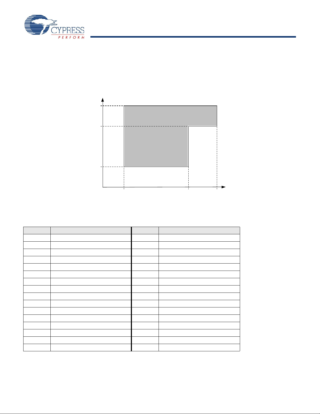
This chapter presents the DC and AC electrical sp ecifications of the CY8C27x43 PSoC device. For the most up to date electrical
specifications, confirm that you have the most recent data sheet by going to the web at http://www.cypress.com/psoc.
Specifications are valid for -40°C ≤ T
12 MHz are valid for -40°C ≤ T
≤ 85°C and TJ ≤ 100°C, except where noted. Specifications for devices running at greater than
A
≤ 70°C and TJ ≤ 82°C.
A
Figure 10. Voltage versus CPU Frequency
The following table lists the units of measure that are used in this chapter.
Table 13. Units of Measure
Symbol Unit of Measure Symbol Unit of Measure
o
C degree Celsius μW microwatts
dB decibels mA milli-ampere
fF femto farad ms milli-second
Hz hertz mV milli-volts
KB 1024 bytes nA nanoampere
Kbit 1024 bits ns nanosecond
kHz kilohertz nV nanovolts
kΩ kilohm W ohm
MHz megahertz pA picoampere
MΩ megaohm pF picofarad
μA microampere pp peak-to-peak
μF microfarad ppm parts per million
μH microhenry ps picosecond
μs microsecond sps samples per second
μV microvolts s sigma: one standard deviation
μVrms microvolts root-mean-square V volts
Document Number: 38-12012 Rev. *O Page 19 of 53
[+] Feedback
Page 20

CY8C27143, CY8C27243
CY8C27443, CY8C27543, CY8C27643
Absolute Maximum Ratings
Exceeding maximum ratings may shorten the useful life of the device. User guidelines are not tested.
Table 14. Absolute Maximum Ratings
Symbol Description Min Typ Max Unit Notes
T
STG
Storage Temperature -55 25 +100
o
C Higher storage temperatures reduce
data retention time. Recommended
storage temperature is +25°C ±
25°C. Extended duration storage
temperatures above 65
reliability.
T
A
Ambient Temperature with Power Applied -40 – +85
o
C
Vdd Supply Voltage on Vdd Relative to Vss -0.5 – +6.0 V
V
IO
V
IOZ
I
MIO
I
MAIO
DC Input Voltage Vss- 0.5 – Vdd + 0.5 V
DC Voltage Applied to Tri-state Vss -
– Vdd + 0.5 V
0.5
Maximum Current into any Port Pin -25 – +50 mA
Maximum Current into any Port Pin Configured
-50 – +50 mA
as Analog Driver
ESD Electro Static Discharge Voltage 2000 – – V Human Body Model ESD.
LU L atch up Curren t – – 200 mA
Operating Temperature
Table 15. Operating Temperature
o
C degrade
Symbol Description Min Typ Max Unit Notes
T
A
T
J
Ambient Temperature -40 – +85
Junction Temperature -40 – +100
o
C
o
C The temperature rise from ambient
to junction is package specific. See
“Thermal Impedances” on page 46.
The user must limit the power
consumption to comply with this
requirement.
Document Number: 38-12012 Rev. *O Page 20 of 53
[+] Feedback
Page 21

CY8C27143, CY8C27243
CY8C27443, CY8C27543, CY8C27643
DC Electrical Characteristics
Notes
3. Standby current includes all functions (POR, LVD, WDT, Sleep Time) needed for reliable system operation. This must be compared with devices that have similar
functions enabled.
4. Refer to the “Ordering Information” on page 50.
DC Chip-Level Specifications
The following table lists guaranteed maximum and min imum specific ations for the voltage and tem perature ranges: 4.75V to 5.25 V
and -40°C ≤ T
are for design guidance only.
Table 16. DC Chip-Level Specifications
Symbol Description Min Typ Max Unit Notes
Vdd Supply Voltage 3.00 – 5.25 V
I
DD
I
DD3
I
SB
I
SBH
I
SBXTL
I
SBXTLH
V
REF
V
REF
≤ 85°C, or 3.0V to 3.6V and -40°C ≤ TA ≤ 85°C, respectively. Typical parameters apply to 5V and 3.3V at 25°C and
A
Supply Current – 5 8 mA Conditions are Vdd = 5.0V , TA = 25 oC,
CPU = 3 MHz, SYSCLK doubler
disabled. VC1 = 1.5 MHz,
VC2 = 93.75 kHz, VC3 = 93.75 kHz.
Supply Current – 3.3 6.0 mA Conditions are Vdd = 3.3V , TA = 25 oC,
CPU = 3 MHz, SYSCLK doubler
disabled. VC1 = 1.5 MHz,
VC2 = 93.75 kHz, VC3 = 93.75 kHz.
Sleep (Mode) Current with POR, LVD, Sleep
Timer, and WDT.
[3]
– 3 6.5 μA Conditions are with inte rnal slow
speed oscillator, Vdd = 3.3V,
-40 oC ≤ TA ≤ 55 oC.
Sleep (Mode) Current with POR, LVD, Sleep
Timer, and WDT at high temperature.
[3]
– 4 25 μA Conditions are with inte rnal slow
speed oscillator, Vdd = 3.3V,
55 oC < TA ≤ 85 oC.
Sleep (Mode) Current with POR, LVD, Sleep
Timer, WDT, and external crystal.
[3]
– 4 7.5 μA Conditions are with properly loaded, 1
μW max, 32.768 kHz crystal.
Vdd = 3.3V, -40 oC ≤ TA ≤ 55 oC.
Sleep (Mode) Current with POR, LVD, Sleep
Timer, WDT, and external crystal at high
temperature.
Reference Voltage (Bandgap) for Silicon A
[3]
[4]
Reference Voltage (Bandgap) for Silicon B
– 5 26 μA Conditions are with properly loaded, 1
μW max, 32.768 kHz crystal.
Vdd = 3.3V, 55 oC < TA ≤ 85 oC.
1.275 1.300 1.325 V Trimmed for appropriate Vdd.
[4]
1.280 1.300 1.320 V Trimmed for appropriate Vdd.
DC General Purpose I/O Specifications
The following table lists guaranteed maximum and min imum specific ations for the voltage and tem perature ranges: 4.75V to 5.25 V
and -40°C ≤ T
are for design guidance only.
≤ 85°C, or 3.0V to 3.6V and -40°C ≤ TA ≤ 85°C, respectively. Typical parameters apply to 5V and 3.3V at 25°C and
A
Table 17. DC GPIO Specifications
Symbol Description Min Typ Max Unit Notes
R
PU
R
PD
V
OH
Pull up Resistor 4 5.6 8 kΩ
Pull down Resistor 4 5.6 8 kΩ
High Output Level Vdd -
– – V IOH = 10 mA, Vdd = 4.75 to 5.25V
1.0
(8 total loads, 4 on even port pins (for
example, P0[2], P1[4]), 4 on odd port
pins (for example, P0[3], P1[5])).
V
OL
Low Output Level – – 0.75 V IOL = 25 mA, Vdd = 4.75 to 5.25V (8
total loads, 4 on even port pins (for
example, P0[2], P1[4]), 4 on odd port
pins (for example, P0[3], P1[5])).
Document Number: 38-12012 Rev. *O Page 21 of 53
[+] Feedback
Page 22

CY8C27143, CY8C27243
CY8C27443, CY8C27543, CY8C27643
Table 17. DC GPIO Specifications (continued)
Symbol Description Min Typ Max Unit Notes
I
I
V
V
V
I
C
C
OH
OL
IL
IH
H
IL
IN
OUT
High Level Source Current 10 – – mA VOH = Vdd-1.0V , see the limitations of
the total current in the note for VOH
Low Level Sink Current 25 – – mA VOL = 0.75V , see the limitations of the
total current in the note for VOL
Input Low Level – – 0.8 V Vdd = 3.0 to 5.25
Input High Level 2.1 – V Vdd = 3.0 to 5.2 5
Input Hysterisis – 60 – mV
Input Leakage (Absolute Value) – 1 – nA Gross teste d to 1 μA.
Capacitive Load on Pins as Input – 3.5 10 pF Package and pin dependent.
Temp = 25
Capacitive Load on Pins as Output – 3.5 10 pF Package and pin dependent.
Temp = 25
o
C.
o
C.
DC Operational Amplifier Specifications
The following tables list guaranteed maximum and minimum specifications for the voltage and temperature ranges: 4.75V to 5.25 V
and -40°C ≤ TA ≤ 85°C, or 3.0V to 3.6V and -40°C ≤ TA ≤ 85°C, respectively. Typical parameters apply to 5V and 3.3V at 25°C and
are for design guidance only.
The Operational Amplifier is a component of both the Analog Continuous Time PSoC blocks and the Analo g Switched Cap PSoC
blocks. The guaranteed specifications are measured in the Analog Continuous Time PSoC block. Typical parameters apply to 5V at
25°C and are for design guidance only.
Table 18. 5V DC Operational Amplifier Specifications
Symbol Description Min Typ Max Unit Notes
V
OSOA
TCV
I
EBOA
C
INOA
V
CMOA
Input Offset Voltage (absolute value)
Power = Low, Opamp Bias = High
Power = Medium, Opamp Bias = High
Power = High, Opamp Bias = High
Average Input Offset Voltage Drift – 7.0 35.0 μV/oC
OSOA
–1.6
–
–
1.3
1.2
10
8
7.5
mV
mV
mV
Input Leakage Current (Port 0 Analog Pins) – 20 – pA Gross tested to 1 μA.
Input Capacitance (Port 0 Analog Pins) – 4.5 9.5 pF Package and pin dependent.
Temp = 25
Common Mode Voltage Range
Common Mode Voltage Range (high power or
high opamp bias)
0.0 – Vdd
0.5 –
Vdd - 0.5
VVThe common-mode input
voltage range is measured
through an analog output
o
C.
buffer. The specification
includes the limitations
imposed by the characteristics
of the analog output buffer.
CMRR
Common Mode Rejection Ratio
OA
Power = Low
Power = Medium
Power = High
60
60
60
– – dB Specification is applicable at
high power. For all other bias
modes (except high power,
high opamp bias), minimum is
60 dB.
G
OLOA
Open Loop Gain
Power = Low
Power = Medium
Power = High
60
60
80
– – dB Specification is applicable at
high power. For all other bias
modes (except high power,
high opamp bias), minimum is
60 dB.
V
OHIGHOA
High Output Voltage Swing (internal signals)
Power = Low
Power = Medium
Power = High
Vdd - 0.2
Vdd - 0.2
Vdd - 0.5
–
–
–
–
–
–
V
V
V
Document Number: 38-12012 Rev. *O Page 22 of 53
[+] Feedback
Page 23

CY8C27143, CY8C27243
CY8C27443, CY8C27543, CY8C27643
Table 18. 5V DC Operational Amplifier Specifications (continued)
Symbol Description Min Typ Max Unit Notes
V
OLOWOA
I
SOA
Low Output Voltage Swing (internal signals)
Power = Low
Power = Medium
Power = High
Supply Current (including associated AGND
buffer)
Power = Low, Opamp Bias = Low
Power = Low, Opamp Bias = High
Power = Medium, Opamp Bias = Low
Power = Medium, Opamp Bias = High
Power = High, Opamp Bias = Low
–
–
–
–
–
–
–
–
–
–
–
–
150
300
600
1200
2400
4600
0.2
0.2
0.5
200
400
800
1600
3200
6400
V
V
V
μA
μA
μA
μA
μA
μA
Power = High, Opamp Bias = High
PSRR
Supply Voltage Rejection Ratio 60 – – dB Vss ≤ VIN ≤ (Vdd - 2.25) or
OA
(Vdd - 1.25V) ≤ VIN ≤ Vdd.
Table 19. 3.3V DC Operational Amplifier Specifications
Symbol Description Min Typ Max Unit Notes
V
OSOA
Input Offset Voltage (absolute value)
Power = Low, Opamp Bias = High
Power = Medium, Opamp Bias = High
–
–
1.65
1.32
10
8
mV
mV
High Power is 5 Volts Only
TCV
I
EBOA
C
INOA
V
CMOA
Average Input Offset Voltage Drift – 7.0 35.0 μV/oC
OSOA
Input Leakage Current (Port 0 Analog Pins) – 20 – pA Gross tested to 1 μA.
Input Capacitance (Port 0 Analog Pins) – 4.5 9.5 pF Package and pin dependent.
Temp = 25
o
C.
Common Mode Voltage Range 0.2 – Vdd - 0.2 V The common-mode input
voltage range is measured
through an analog output
buffer. The specification
includes the limitations
imposed by the characteristics
of the analog output buffer.
CMRR
Common Mode Rejection Ratio
OA
Power = Low
Power = Medium
Power = High
50
50
50
–
–
–
–
–
–
Specification is applicable at
dB
high power. For all other bias
dB
modes (except high power,
dB
high opamp bias), minimum is
60 dB.
G
OLOA
Open Loop Gain
Power = Low
Power = Medium
Power = High
60
60
80
–
–
–
–
–
–
Specification is applicable at
dB
high power. For all other bias
dB
modes (except high power,
dB
high opamp bias), minimum is
60 dB.
V
OHIGHOA
High Output Voltage Swing (internal signals)
Power = Low
Power = Medium
Power = High is 5V only
Vdd - 0.2
Vdd - 0.2
Vdd - 0.2
–
–
–
–
–
–
V
V
V
Document Number: 38-12012 Rev. *O Page 23 of 53
[+] Feedback
Page 24

CY8C27143, CY8C27243
CY8C27443, CY8C27543, CY8C27643
Table 19. 3.3V DC Operational Amplifier Specifications (continued)
Symbol Description Min Typ Max Unit Notes
V
OLOWOA
I
SOA
PSRR
Low Output Voltage Swing (internal signals)
Power = Low
Power = Medium
Power = High
–
–
–
–
–
–
0.2
0.2
0.2
V
V
V
Supply Current (including associated AGND
buffer)
Power = Low, Opamp Bias = Low
Power = Low, Opamp Bias = High
Power = Medium, Opamp Bias = Low
Power = Medium, Opamp Bias = High
Power = High, Opamp Bias = Low
Power = High, Opamp Bias = High
Supply Voltage Rejection Ratio 50 80 – dB Vss ≤ VIN ≤ (Vdd - 2.25) or
OA
–
–
–
–
–
–
150
300
600
1200
2400
4600
200
400
800
1600
3200
6400
μA
μA
μA
μA
μA
μA
(Vdd - 1.25V) ≤ VIN ≤ Vdd.
DC Low Power Comparator Specifications
The following table lists guaranteed maximum and min imum specific ations for the voltage and tem perature ranges: 4.75V to 5.25 V
and -40°C ≤ T
apply to 5V at 25°C and are for design guidance only.
≤ 85°C, 3.0V to 3.6V and -40°C ≤ TA ≤ 85°C, or 2.4V to 3.0V and -40°C ≤ TA ≤ 85°C, respectively . Typical parameters
A
Table 20. DC Low Power Comparator Specifications
Symbol Description Min Typ Max Unit
V
REFLPC
I
SLPC
V
OSLPC
Low power comparator (LPC) reference
voltage range
LPC supply current – 10 40 μA
LPC voltage offset – 2.5 30 mV
0.2 – Vdd - 1 V
DC Analog Output Buffer Specifications
The following tables list guaranteed maximum and minimum specifications for the voltage and temperature ranges: 4.75V to 5.25 V
and -40°C ≤ T
are for design guidance only.
≤ 85°C, or 3.0V to 3.6V and -40°C ≤ TA ≤ 85°C, respectively. Typical parameters apply to 5V and 3.3V at 25°C and
A
Table 21. 5V DC Analog Output Buffer Specifications
Symbol Description Min Typ Max Unit
V
OSOB
TCV
OSOB
V
CMOB
R
OUTOB
V
OHIGHOB
V
OLOWOB
I
SOB
PSRR
I
OMAX
OB
Input Offset Voltage (Absolute Value) – 3 12 mV
Average Input Offset Voltage Drift – +6 – μV/°C
Common-Mode Input Voltage Range 0.5 – Vdd - 1.0 V
Output Resistance
Power = Low
Power = High
–
–
1
1
–
–
W
W
High Output Voltage Swing (Load = 32 ohms
to Vdd/2)
Power = Low
Power = High
0.5 x Vdd + 1.3
0.5 x Vdd
+ 1.3
–
–
–
–
V
V
Low Output Voltage Swing (Load = 32 ohms
to Vdd/2)
Power = Low
Power = High
–
–
––0.5 x Vdd - 1.3
0.5 x Vdd
- 1.3
V
V
Supply Current Including Bias Cell (No Load)
Power = Low
Power = High
–
–
1.1
2.6
5.1
8.8
mA
mA
Supply Voltage Rejection Ratio 60 64 – dB
Maximum Output Current – 40 – mA
Document Number: 38-12012 Rev. *O Page 24 of 53
[+] Feedback
Page 25

CY8C27143, CY8C27243
CY8C27443, CY8C27543, CY8C27643
Table 22. 3.3V DC Analog Output Buffer Specifications
Note
5. L
1
= 2 mH inductor, C1 = 10 mF capacitor, D1 = Schottky diode. See Figure 11.
Symbol Description Min Typ Max Units
V
OSOB
TCV
OSOB
V
CMOB
R
OUTOB
V
OHIGHOB
V
OLOWOB
I
SOB
PSRR
OB
Input Offset Voltage (Absolute Value) – 3 12 mV
Average Input Offset Voltage Drift – +6 – μV/°C
Common-Mode Input Voltage Range 0.5 - Vdd - 1.0 V
Output Resistance
Power = Low
Power = High
–
–
1
1
–
–
W
W
High Output Voltage Swing (Load = 1k ohms
to Vdd/2)
Power = Low
Power = High
0.5 x Vdd + 1.0
0.5 x Vdd
+ 1.0
–
–
–
–
V
V
Low Output Voltage Swing (Load = 1k ohms
to Vdd/2)
Power = Low
Power = High
–
–
–
–
0.5 x Vdd - 1.0
0.5 x Vdd
- 1.0
V
V
Supply Current Including Bias Cell (No Load)
Power = Low
Power = High –
0.8
2.0
2.0
4.3
mA
mA
Supply Voltage Rejection Ratio 60 64 – dB
DC Switch Mode Pump Specifications
The following table lists guaranteed maximum and min imum specific ations for the voltage and tem perature ranges: 4.75V to 5.25 V
and -40°C ≤ TA ≤ 85°C, or 3.0V to 3.6V and -40°C ≤ TA ≤ 85°C, respectively. Typical parameters apply to 5V and 3.3V at 25°C and
are for design guidance only.
Table 23. DC Switch Mode Pump (SMP) Specifications
Symbol Description Min Typ Max Unit Notes
V
5V 5V Output Voltage 4.75 5.0 5.25 V Configuration of footnote.
PUMP
neglecting ripple. SMP trip voltage is
set to 5.0V.
V
3V 3V Output Voltage 3.00 3.25 3.60 V Configuration of footnote.
PUMP
neglecting ripple. SMP trip voltage is
set to 3.25V.
I
PUMP
V
5V Input Voltage Range from Battery 1.8 – 5.0 V Configuration of footnote.
BAT
V
3V Input Voltage Range from Battery 1.0 – 3.3 V Configuration of footnote.
BAT
V
BATSTART
ΔV
PUMP_Line
Available Output Current
V
V
BAT
BAT
= 1.5V, V
= 1.8V, V
PUMP
PUMP
= 3.25V
= 5.0V
Minimum Input Voltage from Battery to
Start Pum p
Line Regulation (over V
range) – 5 – %VOConfiguration of footnote.
BAT
8
5
–
–
–
–
1.1 – – V Configuration of footnote.
Configuration of footnote.
SMP trip voltage is set to 3.25V.
mA
SMP trip voltage is set to 5.0V.
mA
voltage is set to 5.0V.
voltage is set to 3.25V.
“Vdd Value for PUMP Trip” specified
by the VM[2:0] setting in the DC POR
and LVD Specification, Table 29 on
page 30.
[5]
Average,
[5]
Average,
[5]
[5]
SMP trip
[5]
SMP trip
[5]
[5]
VO is the
Document Number: 38-12012 Rev. *O Page 25 of 53
[+] Feedback
Page 26

CY8C27143, CY8C27243
CY8C27443, CY8C27543, CY8C27643
Table 23. DC Switch Mode Pump (SMP) Specifications (continued)
Battery
C1
D1
+
PSoC
TM
Vdd
Vss
SMP
V
BAT
V
PUMP
L
1
Note
6. AGND tolerance includes the offsets of the local buffer in the PSoC block.
Symbol Description Min Typ Max Unit Notes
ΔV
PUMP_Load
Load Regulation – 5 – %VOConfiguration of footnote.
“Vdd Value for PUMP Trip” specified
by the VM[2:0] setting in the DC POR
and LVD Specification, Table 29 on
page 30.
ΔV
PUMP_Ripple
E
3
F
PUMP
DC
PUMP
Output Voltage Ripple (depends on
capacitor/load)
– 100 – mVpp Configuration of footnote.
mA.
Efficiency 35 50 – % Configuration of footnote.
mA. SMP trip voltage is set to 3.25V.
Switching Frequency – 1.3 – MHz
Switching Duty Cycle – 50 – %
Figure 11. Basic Switch Mode Pump Circuit
[5]
VO is the
[5]
Load is 5
[5]
Load is 5
DC Analog Reference Specifications
The following tables list guaranteed maximum and minimum specifications for the voltage and temperature ranges: 4.75V to 5.25 V
and -40°C ≤ T
are for design guidance only.
≤ 85°C, or 3.0V to 3.6V and -40°C ≤ TA ≤ 85°C, respectively. Typical parameters apply to 5V and 3.3V at 25°C and
A
The guaranteed specifications are measured through the Analog Continuous Time PSoC blocks. The power levels for AGND refer to
the power of the Analog Continuous Time PSoC block. The power levels for RefHi and RefLo refer to the Analog Reference Control
register. The limits stated for AGND include the offset error of the AGND buffer local to the Analog Continuous Time PSoC block.
Reference control power is high.
Note Avoid using P2[4] for digital signaling when using an analog resource that depends on the Analog Reference. Some coupling
of the digital signal may appear on the AGND.
Table 24. Silicon Revision A – 5V DC Analog Reference Specifications
Symbol Description Min Typ Max Unit
BG Bandgap Voltage Reference 1.274 1.30 1.326 V
[6]
[6]
[6]
[6]
[6]
[6]
– AGND = Vdd/2
– AGND = 2 x BandGap
– AGND = P2[4] (P2[4] = Vdd/2)
– AGND = BandGap
– AGND = 1.6 x BandGap
– AGND Block to Block Variation
(AGND = Vdd/2)
– RefHi = Vdd/2 + BandGap Vdd/2 + BG - 0.140 Vdd/2 + BG - 0.018 Vdd/2 + BG + 0.103 V
– RefHi = 3 x BandGap 3 x BG - 0.112 3 x BG - 0.018 3 x BG + 0.076 V
Document Number: 38-12012 Rev. *O Page 26 of 53
Vdd/2 - 0.030 Vdd/2 - 0.004 Vdd/2 + 0.003 V
2 x BG - 0.043 2 x BG - 0.010 2 x BG + 0.024 V
P2[4] - 0.013 P2[4] P2[4] + 0.014 V
BG - 0.009 BG BG + 0.009 V
1.6 x BG - 0.018 1.6 x BG 1.6 x BG + 0.018 V
-0.034 0.000 0.034 V
[+] Feedback
Page 27

CY8C27143, CY8C27243
CY8C27443, CY8C27543, CY8C27643
Table 24. Silicon Revision A – 5V DC Analog Reference Specifications (continued)
Symbol Description Min Typ Max Unit
– RefHi = 2 x BandGap + P2[6]
(P2[6] = 1.3V)
– RefHi = P2[4] + BandGap
(P2[4] = Vdd/2)
– RefHi = P2[4] + P2[6] (P2[4] = Vdd/2,
P2[6] = 1.3V)
– RefHi = 3.2 x BandGap 3.2 x BG - 0.112 3.2 x BG 3.2 x BG + 0.076 V
– RefLo = Vdd/2 – BandGap Vdd/2 - BG - 0.051 Vdd/2 - BG + 0.024 Vdd/2 - BG + 0.098 V
– RefLo = BandGap BG - 0.082 BG + 0.023 BG + 0.129 V
– RefLo = 2 x BandGap - P2[6]
(P2[6] = 1.3V)
– RefLo = P2[4] – BandGap
(P2[4] = Vdd/2)
– RefLo = P2[4]-P2[6] (P2[4] = Vdd/2,
P2[6] = 1.3V)
2 x BG + P2[6] - 0.113 2 x BG + P2[6] - 0.018 2 x BG + P2[6] + 0.077 V
P2[4] + BG - 0.130 P2[4] + BG - 0.016 P2[4] + BG + 0.098 V
P2[4] + P2[6] - 0.133 P2[4] + P2[6] - 0.016 P2[4] + P2[6] + 0.100 V
2 x BG - P2[6] - 0.084 2 x BG - P2[6] + 0.025 2 x BG - P2[6] + 0.134 V
P2[4] - BG - 0.056 P2[4] - BG + 0.026 P2[4] - BG + 0.107 V
P2[4] - P2[6] - 0.057 P2[4] - P2[6] + 0.026 P2[4] - P2[6] + 0.110 V
Document Number: 38-12012 Rev. *O Page 27 of 53
[+] Feedback
Page 28

CY8C27143, CY8C27243
CY8C27443, CY8C27543, CY8C27643
Note
7.
AGND tolerance includes the offsets of the local buffer in the PSoC block.
Table 25. Silicon Revision B – 5V DC Analog Reference Specifications
Symbol Description Min Typ Max Unit
BG Bandgap Voltage Reference 1.28 1.30 1.32 V
– AGND = Vdd/2
– AGND = 2 x BandGap
– AGND = P2[4] (P2[4] = Vdd/2)
– AGND = BandGap
– AGND = 1.6 x BandGap
– AGND Block to Block Variation
(AGND = Vdd/2)
[7]
[7]
[7]
[7]
[7]
[7]
2 x BG - 0.043 2 x BG 2 x BG + 0.024 V
P2[4] - 0.011 P2[4] P2[4] + 0.011 V
BG - 0.009 BG BG + 0.009 V
1.6 x BG - 0.018 1.6 x BG 1.6 x BG + 0.018 V
-0.034 0.000 0.034 V
Vdd/2 - 0.030 Vdd/2 Vdd/2 + 0.007 V
– RefHi = Vdd/2 + BandGap Vdd/2 + BG - 0.1 Vdd/2 + BG - 0.01 Vdd/2 + BG + 0.1 V
– RefHi = 3 x BandGap 3 x BG - 0.06 3 x BG - 0.01 3 x BG + 0.06 V
– RefHi = 2 x BandGap + P2[6]
2 x BG + P2[6] - 0.06 2 x BG + P2[6] - 0.01 2 x BG + P2[6] + 0.06 V
(P2[6] = 1.3V)
– RefHi = P2[4] + BandGap
P2[4] + BG - 0.06 P2[4] + BG - 0.01 P2[4] + BG + 0.06 V
(P2[4] = Vdd/2)
– RefHi = P2[4] + P2[6] (P2[4] = Vdd/2,
P2[4] + P2[6] - 0.06 P2[4] + P2[6] - 0.01 P2[4] + P2[6] + 0.06 V
P2[6] = 1.3V)
– RefHi = 3.2 x BandGap 3.2 x BG - 0.06 3.2 x BG - 0.01 3.2 x BG + 0.06 V
– RefLo = Vdd/2 – BandGap Vdd/2 - BG - 0.051 Vdd/2 - BG + 0.01 Vdd/2 - BG + 0.06 V
– RefLo = BandGap BG - 0.06 BG + 0.01 BG + 0.06 V
– RefLo = 2 x BandGap - P2[6]
2 x BG - P2[6] - 0.04 2 x BG - P2[6] + 0.01 2 x BG - P2[6] + 0.04 V
(P2[6] = 1.3V)
– RefLo = P2[4] – BandGap
P2[4] - BG - 0.056 P2[4] - BG + 0.01 P2[4] - BG + 0.056 V
(P2[4] = Vdd/2)
– RefLo = P2[4]-P2[6] (P2[4] = Vdd/2,
P2[4] - P2[6] - 0.056 P2[4] - P2[6] + 0.01 P2[4] - P2[6] + 0.056 V
P2[6] = 1.3V)
Table 26. Silicon Revision A – 3.3V DC Analog Reference Specifications
Symbol Description Min Typ Max Unit
BG Bandgap Voltage Reference 1.274 1.30 1.326 V
– AGND = Vdd/2
– AGND = 2 x BandGap
[8]
[8]
Vdd/2 - 0.027 Vdd/2 - 0.003 Vdd/2 + 0.002 V
Not Allowed
– AGND = P2[4] (P2[4] = Vdd/2) P2[4] - 0.008 P2[4] + 0.001 P2[4] + 0.009 V
– AGND = BandGap
– AGND = 1.6 x BandGap
– AGND Block to Block Variation
(AGND = Vdd/2)
[8]
[8]
[8]
BG - 0.009 BG BG + 0.009 V
1.6 x BG - 0.018 1.6 x BG 1.6 x BG + 0.018 V
-0.034 0.000 0.034 V
– RefHi = Vdd/2 + BandGap Not Allowed
– RefHi = 3 x BandGap Not Allowed
– RefHi = 2 x BandGap + P2[6]
Not Allowed
(P2[6] = 0.5V)
– RefHi = P2[4] + BandGap
Not Allowed
(P2[4] = Vdd/2)
– RefHi = P2[4] + P2[6] (P2[4] = Vdd/2,
P2[4] + P2[6] - 0.075 P2[4] + P2[6] - 0.009 P2[4] + P2[6] + 0.057 V
P2[6] = 0.5V)
– RefHi = 3.2 x BandGap Not Allowed
– RefLo = Vdd/2 - BandGap Not Allowed
Document Number: 38-12012 Rev. *O Page 28 of 53
[+] Feedback
Page 29

CY8C27143, CY8C27243
CY8C27443, CY8C27543, CY8C27643
Table 26. Silicon Revision A – 3.3V DC Analog Reference Specifications (continued)
Note
8. AGND tolerance includes the offsets of the local buffer in the PSoC block.
See Application Note AN2012 “Adjusting PSoC Microcontroller Trims for Dual Voltage-Range Operation” for information on trimming for operation at 3.3V.
Symbol Description Min Typ Max Unit
– RefLo = BandGap Not Allowed
– RefLo = 2 x BandGa p - P2[6]
Not Allowed
(P2[6] = 0.5V)
– RefL o = P2[4] – BandGap
Not Allowed
(P2[4] = Vdd/2)
– RefL o = P2[4]-P2[6] (P2[4] = Vdd/2,
P2[4] - P2[6] - 0.048 P2[4] - P2[6] + 0.022 P2[4 ] - P2[6] + 0.092 V
P2[6] = 0.5V)
Table 27. Silicon Revision B – 3.3V DC Analog Reference Specifications
Symbol Description Min Typ Max Unit
BG Bandgap Voltage Reference 1.28 1.30 1.32 V
– AGND = Vdd/2
– AGND = 2 x BandGap
[8]
[8]
Vdd/2 - 0.027 Vdd/2 Vdd/2 + 0.005 V
Not Allowed
– AGND = P2[4] (P2[4] = Vdd/2) P2[4] - 0.008 P2[4] P2[4] + 0.009 V
– AGND = BandGap
– AGND = 1.6 x BandGap
– AGND Block to Block Variation
(AGND = Vdd/2)
[8]
[8]
[8]
BG - 0.009 BG BG + 0.009 V
1.6 x BG - 0.018 1.6 x BG 1.6 x BG + 0.018 V
-0.034 0.000 0.034 mV
– RefHi = Vdd/2 + BandGap Not Allowed
– RefHi = 3 x BandGap Not Allowed
– RefHi = 2 x BandGap + P2[6]
Not Allowed
(P2[6] = 0.5V)
– RefHi = P2[4] + BandGap
Not Allowed
(P2[4] = Vdd/2)
– RefHi = P2[4] + P2[6] (P2[4] = Vdd/2,
P2[4] + P2[6] - 0.06 P2[4] + P2[6] - 0.01 P2[4] + P2[6] + 0.057 V
P2[6] = 0.5V)
– RefHi = 3.2 x BandGap Not Allowed
– RefLo = Vdd/2 - BandGap Not Allowed
– RefLo = BandGap Not Allowed
– RefLo = 2 x BandGa p - P2[6]
Not Allowed
(P2[6] = 0.5V)
– RefL o = P2[4] – BandGap
Not Allowed
(P2[4] = Vdd/2)
– RefL o = P2[4]-P2[6] (P2[4] = Vdd/2,
P2[4] - P2[6] - 0.048 P2[4] - P2[6] + 0.01 P2[4] - P2[6] + 0.048 V
P2[6] = 0.5V)
DC Analog PSoC Block Specifications
The following table lists guaranteed maximum and min imum specific ations for the voltage and tem perature ranges: 4.75V to 5.25 V
and -40°C ≤ T
are for design guidance only.
≤ 85°C, or 3.0V to 3.6V and -40°C ≤ TA ≤ 85°C, respectively. Typical parameters apply to 5V and 3.3V at 25°C and
A
Table 28. DC Analog PSoC Block Specifications
Symbol Description Min Typ Max Unit
R
CT
C
SC
Document Number: 38-12012 Rev. *O Page 29 of 53
Resistor Unit Value (Continuous Time) – 12.2 – kΩ
Capacitor Unit Value (Switch Cap) – 80 – fF
[+] Feedback
Page 30
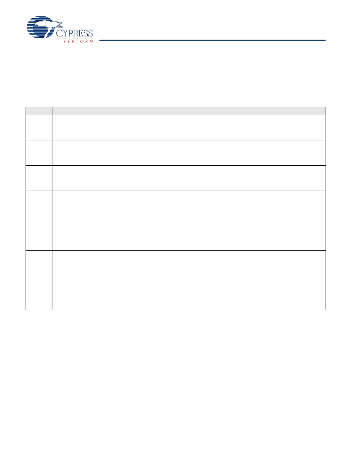
CY8C27143, CY8C27243
CY8C27443, CY8C27543, CY8C27643
DC POR and LVD Specifications
Notes
9. Always greater than 50 mV above PPOR (PORLEV = 00) for falling supply.
10.Always greater than 50 mV above PPOR (PORLEV = 10) for falling supply.
The following table lists guaranteed maximum and min imum specific ations for the voltage and tem perature ranges: 4.75V to 5.25 V
and -40°C ≤ T
are for design guidance only.
≤ 85°C, or 3.0V to 3.6V and -40°C ≤ TA ≤ 85°C, respectively. Typical parameters apply to 5V and 3.3V at 25°C and
A
Note The bits PORLEV and VM in the following table refer to bits in the VLT_CR register. See the PSoC Programmable
System-on-Chip Technical Reference Manual for more information on the VLT_CR register.
Table 29. DC POR and LVD Specifications
Symbol Description Min Typ Max Unit Notes
V
PPOR0R
V
PPOR1R
V
PPOR2R
Vdd Value for PPOR Trip (positive ramp)
PORLEV[1:0] = 00b
PORLEV[1:0] = 01b
PORLEV[1:0] = 10b
–
–
–
2.91
4.39
4.55
–
–
–
Vdd must be greater than or equal
V
to 2.5V during startup, reset from
V
the XRES pin, or reset from
V
Watchdog.
Vdd Value for PPOR Trip (negative ramp)
V
PPOR0
V
PPOR1
V
PPOR2
PORLEV[1:0] = 00b
PORLEV[1:0] = 01b
PORLEV[1:0] = 10b
–
–
–
2.82
4.39
4.55
–
–
–
V
V
V
PPOR Hysteresis
[9]
[10]
mV
mV
mV
V
V
V
V
V
V
V
V
V
V
V
V
V
V
V
V
V
V
V
V
PH0
PH1
PH2
LVD0
LVD1
LVD2
LVD3
LVD4
LVD5
LVD6
LVD7
PORLEV[1:0] = 00b
PORLEV[1:0] = 01b
PORLEV[1:0] = 10b
Vdd Value for LVD Trip
VM[2:0] = 000b
VM[2:0] = 001b
VM[2:0] = 010b
VM[2:0] = 011b
VM[2:0] = 100b
VM[2:0] = 101b
VM[2:0] = 110b
VM[2:0] = 111b
–
–
–
2.86
2.96
3.07
3.92
4.39
4.55
4.63
4.72
92
0
0
2.92
3.02
3.13
4.00
4.48
4.64
4.73
4.81
–
–
–
2.98
3.08
3.20
4.08
4.57
4.74
4.82
4.91
Vdd Value for PUMP Trip
V
PUMP0
V
PUMP1
V
PUMP2
V
PUMP3
V
PUMP4
V
PUMP5
V
PUMP6
V
PUMP7
VM[2:0] = 000b
VM[2:0] = 001b
VM[2:0] = 010b
VM[2:0] = 011b
VM[2:0] = 100b
VM[2:0] = 101b
VM[2:0] = 110b
VM[2:0] = 111b
2.96
3.03
3.18
4.11
4.55
4.63
4.72
4.90
3.02
3.10
3.25
4.19
4.64
4.73
4.82
5.00
3.08
3.16
3.32
4.28
4.74
4.82
4.91
5.10
V
V
V
V
V
V
V
V
V
Document Number: 38-12012 Rev. *O Page 30 of 53
[+] Feedback
Page 31

CY8C27143, CY8C27243
CY8C27443, CY8C27543, CY8C27643
DC Programming Specifications
Notes
11.The 50,000 cycle flash endurance per block will only be guaranteed if the flash is operating within one voltage range. Voltage ranges are 3.0V to 3.6V and 4.75V
to 5.25V.
12.A maximum of 36 x 50,000 block endurance cycles is allowed. This may be balanced between operations on 36x1 blocks of 50,000 maximum cycles each, 36x2
blocks of 25,000 maximum cycles each, or 36x4 blocks of 12,500 maximum cycles each (to limit the total number of cycles to 36x50,000 and that no single block
ever sees more than 50,000 cycles).
For the full industrial range, the user must employ a temperature sensor u ser modu le (FlashTemp) and feed th e result t o the t emp er ature ar gument be for e writing.
Refer to the Flash APIs Application Note AN2015 at http://www.cypress.com under Application Notes for more information
The following table lists guaranteed maximum and min imum specific ations for the voltage and tem perature ranges: 4.75V to 5.25 V
and -40°C ≤ T
are for design guidance only.
≤ 85°C, or 3.0V to 3.6V and -40°C ≤ TA ≤ 85°C, respectively. Typical parameters apply to 5V and 3.3V at 25°C and
A
Table 30. DC Programming Specifications
Symbol Description Min Typ Max Unit Notes
I
DDP
V
ILP
V
IHP
I
ILP
I
IHP
V
OLV
V
OHV
Flash
Flash
Flash
Supply Current During Programming or Verify – 5 25 mA
Input Low Voltage During Programming or
– – 0.8 V
Verify
Input High Voltage During Programming or
2.2 – – V
Verify
Input Current when Applying Vilp to P1[0] or
– – 0.2 mA Driving internal pull down
P1[1] During Programming or Verify
Input Current when Applying Vihp to P1[0] or
– – 1.5 mA Driving internal pull down
P1[1] During Programming or Verify
Output Low Voltage During Programming or
– – Vss +
Verify
Output High Voltage During Programming or
Vdd - 1.0 – Vdd V
Verify
Flash Endurance (per block) 50,000
ENPB
Flash Endurance (total)
ENT
Flash Data Retention 10 – – Years
DR
[12]
[11]
– – Cycles Erase/write cycles per
1,800,000 – – Cycles Erase/write cycles.
resistor.
resistor.
V
0.75
block.
Document Number: 38-12012 Rev. *O Page 31 of 53
[+] Feedback
Page 32

CY8C27143, CY8C27243
CY8C27443, CY8C27543, CY8C27643
AC Electrical Characteristics
Notes
13.4.75V < Vdd < 5.25V.
14.Accuracy derived from Internal Main Oscillator with appropriate trim for Vdd range.
15.3.0V < Vdd < 3.6V. See Application Note AN2 012 “Adjusting PSoC Microcontroller Trims for Dual V olt age-Range Operation” for informa tion on trimming for operat ion
at 3.3V.
16.See the individual user module data sheets for information on maximum frequencies for user modules.
AC Chip-Level Specifications
The following table lists guaranteed maximum and min imum specific ations for the voltage and tem perature ranges: 4.75V to 5.25 V
and -40°C ≤ T
are for design guidance only.
Table 31. AC Chip-Level Specifications
≤ 85°C, or 3.0V to 3.6V and -40°C ≤ TA ≤ 85°C, respectively. Typical parameters apply to 5V and 3.3V at 25°C and
A
Symbol Description Min Typ Max Unit Notes
F
F
F
F
F
F
F
IMO
CPU1
CPU2
48M
24M
32K1
32K2
Internal Main Oscillator Frequency 23.4 24 24.6
CPU Frequency (5V Nominal) 0.93 24 24.6
CPU Frequency (3.3V Nominal) 0.93 12 12.3
Digital PSoC Block Frequency 0 48 49.2
Digital PSoC Block Frequency 0 24 24.6
Internal Low Speed Oscillator
15 32 64 kHz
Frequency
External Crystal Oscillator – 32.768 – kHz Accuracy is capacitor and
[13]
[13,14]
[14,15]
[13,14, 16]
[14, 16]
MHz Trimmed. Utilizing factory trim
values.
MHz Trimmed. Utilizing factory trim
values.
MHz Trimmed. Utilizing factory trim
values.
MHz Refer to the AC Digital Block
Specifications below.
MHz
crystal dependent. 50% duty
cycle.
F
Inte rnal Low Speed Oscillator (ILO)
32K_U
Untrimmed Frequency
5 – – kHz After a reset and before the
m8c starts to run, the ILO is not
trimmed. See the System
Resets section of the PSoC
Technical Reference Manual
for details on timing this
F
PLL
Jitter
24M2
T
PLLSLEW
T
PLLSLEWSLOW
T
OS
T
OSACC
PLL Frequency – 23.986 – MHz Multiple (x732) of crystal
frequency.
24 MHz Period Jitter (PLL) – – 600 ps
PLL Lock Time 0.5 – 10 ms
PLL Lock Time for Low Gain Setting 0.5 – 50 ms
External Crystal Oscillator Startup to
– 1700 2620 ms
1%
External Crystal Oscillator Startup to
100 ppm
– 2800 3800 ms The crystal oscillator frequency
is within 100 ppm of its final
value by the end of the T
period. Correct operation
assumes a properly loaded 1
µW maximum drive level
32.768 kHz crystal. 3.0V ≤ Vdd
≤ 5.5V,
-40°C ≤ T
Jitter
T
XRST
DC
DC
Step
32k
24M
ILO
24M
32 kHz Period Jitter – 100 – ns
External Reset Pulse Width 10 – – μs
24 MHz Duty Cycle 40 50 60 %
Internal Low Speed Oscillator Duty
20 50 80 %
Cycle
24 MHz Trim Step Size – 50 – kHz
≤ 85°C.
A
osacc
Document Number: 38-12012 Rev. *O Page 32 of 53
[+] Feedback
Page 33

CY8C27143, CY8C27243
CY8C27443, CY8C27543, CY8C27643
Table 31. AC Chip-Level Specifications (continued)
24 MHz
F
PLL
PLL
Enable
T
PLLSLEW
PLL
Gain
0
24 MHz
F
PLL
PLL
Enable
T
PLLSLEWLOW
PLL
Gain
1
32 kHz
F
32K2
32K
Select
T
OS
Jitter24M1
F
24M
Jitter32k
F
32K2
Symbol Description Min Typ Max Unit Notes
T
POWERUP
Time from end of POR to CPU
executing code
– 16 100 ms Power up from 0V. See the
System Resets section of the
PSoC Technical Reference
Manual.
Fout
48M
Jitter
24M1
F
MAX
SR
POWER_UP
48 MHz Output Frequency 46.8 48.0 49.2
24 MHz Period Jitter (IMO) – 600 – ps
Maximum frequency of signal on row
– – 12.3 MHz
input or row output.
Power Supply Slew Rate – – 250 V/ms Vdd slew rate during power up.
[13,15]
MHz Trimmed. Utilizing factory trim
values.
Figure 12. PLL Lock Timing Diagram
Figure 13. PLL Lock for Low Gain Setting Timing Diagram
Figure 14. External Crystal Oscillator Startup Timing Diagram
Figure 15. 24 MHz Period Jitter (IMO) Timing Diagram
Figure 16. 32 kHz Period Jitter (ECO) Timing Diagram
Document Number: 38-12012 Rev. *O Page 33 of 53
[+] Feedback
Page 34

CY8C27143, CY8C27243
CY8C27443, CY8C27543, CY8C27643
AC General Purpose I/O Specifications
TFallF
TFallS
TRiseF
TRiseS
90%
10%
GPIO
Pin
Output
Voltage
The following table lists guaranteed maximum and min imum specific ations for the voltage and tem perature ranges: 4.75V to 5.25 V
and -40°C ≤ T
are for design guidance only.
≤ 85°C, or 3.0V to 3.6V and -40°C ≤ TA ≤ 85°C, respectively. Typical parameters apply to 5V and 3.3V at 25°C and
A
Table 32. AC GPIO Specifications
Symbol Description Min Typ Max Unit Notes
F
T
T
T
T
GPIO
RiseF
FallF
RiseS
FallS
GPIO Operating Frequency 0 – 12 MHz Normal Strong Mode
Rise Time, Normal Strong Mode, Cload = 50 pF 3 – 18 ns Vdd = 4.5 to 5.25V, 10% - 90%
Fall Time, Normal Strong Mode, Cload = 50 pF 2 – 18 ns Vdd = 4.5 to 5.25V , 10% - 90%
Rise Time, Slow Strong Mode, Cload = 50 pF 10 27 – ns Vdd = 3 to 5.25 V, 10% - 90%
Fall Time, Slow Strong Mode, Cload = 50 pF 10 22 – ns Vdd = 3 to 5.25V, 10% - 90%
Figure 17. GPIO Timing Diagram
AC Operational Amplifier Specifications
The following tables list guaranteed maximum and minimum specifications for the voltage and temperature ranges: 4.75V to 5.25 V
and -40°C ≤ T
are for design guidance only.
≤ 85°C, or 3.0V to 3.6V and -40°C ≤ TA ≤ 85°C, respectively. Typical parameters apply to 5V and 3.3V at 25°C and
A
Settling times, slew rates, and gain bandwidth are based on the Analog Continuous Time PSoC block.
Power = High and Opamp Bias = High is not supported at 3.3V.
Table 33. 5V AC Operational Amplifier Specifications
Symbol Description Min Typ Max Unit
Rising Settling Time from 80% of ΔV to 0.1% of ΔV (10 pF load, Unity Gain)
Power = Low, Opamp Bias = Low
Power = Medium, Opamp Bias = High
Power = High, Opamp Bias = High
Falling Settling Time from 20% of ΔV to 0.1% of ΔV (10 pF load, Unity Gain)
Power = Low, Opamp Bias = Low
Power = Medium, Opamp Bias = High
Power = High, Opamp Bias = High
Rising Slew Rate (20% to 80%)(10 pF load, Unity Gain)
Power = Low, Opamp Bias = Low
Power = Medium, Opamp Bias = High
Power = High, Opamp Bias = High
Falling Slew Rate (20% to 80%)(10 pF load, Unity Gain)
Power = Low, Opamp Bias = Low
Power = Medium, Opamp Bias = High
Power = High, Opamp Bias = High
–
–
–
–
–
–
0.15
1.7
6.5
0.01
0.5
4.0
–
–
–
–
–
–
–
–
–
–
–
–
3.9
0.72
0.62
5.9
0.92
0.72
–
–
–
–
–
–
T
T
SR
SR
ROA
SOA
ROA
FOA
μs
μs
μs
μs
μs
μs
V/μs
V/μs
V/μs
V/μs
V/μs
V/μs
Document Number: 38-12012 Rev. *O Page 34 of 53
[+] Feedback
Page 35

CY8C27143, CY8C27243
CY8C27443, CY8C27543, CY8C27643
Table 33. 5V AC Operational Amplifier Specifications (continued)
100
1000
10000
0.001 0.01 0.1 1 10 100Freq (kHz)
dBV/rtHz
0
0.01
0.1
1.0
10
Symbol Description Min Typ Max Unit
BW
E
NOA
OA
Gain Bandwidth Product
Power = Low, Opamp Bias = Low
Power = Medium, Opamp Bias = High
Power = High, Opamp Bias = High
0.75
3.1
5.4
–
–
–
–
–
–
MHz
MHz
MHz
Noise at 1 kHz (Power = Medium, Opamp Bias = High) – 100 – nV/rt-Hz
Table 34. 3.3V AC Operational Amplifier Specifications
Symbol Description Min Typ Max Units
T
ROA
T
SOA
SR
SR
BW
E
NOA
Rising Settling Time from 80% of ΔV to 0.1% of ΔV (10 pF load, Unity Gain)
Power = Low, Opamp Bias = Low
Power = Low, Opamp Bias = High
–
–
–
–
Falling Settling Time from 20% of ΔV to 0.1% of ΔV (10 pF load, Unity Gain)
Power = Low, Opamp Bias = Low
Power = Medium, Opamp Bias = High
Rising Slew Rate (20% to 80%)(10 pF load, Unity Gain)
ROA
Power = Low, Opamp Bias = Low
Power = Medium, Opamp Bias = High
Falling Slew Rate (20% to 80%)(10 pF load, Unity Gain)
FOA
Power = Low, Opamp Bias = Low
Power = Medium, Opamp Bias = High
Gain Bandwidth Product
OA
Power = Low, Opamp Bias = Low
Power = Medium, Opamp Bias = High
–
–
0.31
2.7
0.24
1.8
0.67
2.8
–
–
–
–
–
–
–
–
Noise at 1 kHz (Power = Medium, Opamp Bias = High) – 100 – nV/rt-Hz
3.92
0.72
5.41
0.72
–
–
–
–
–
–
V/μs
V/μs
V/μs
V/μs
MHz
MHz
μs
μs
μs
μs
When bypassed by a capacitor on P2[4], the noise of the analog ground signal distributed to each block is reduced by a factor of up
to 5 (14 dB). This is at frequencies above the corner frequency defined by the on-chip 8.1k resistance and the external capacitor.
Figure 18. Typical AGND Noise with P2[4] Bypass
At low frequencies, the opamp noise is proportional to 1/f, power independent, and determined by device geometry. At high
frequencies, increased power level reduces the noise spectrum level.
Document Number: 38-12012 Rev. *O Page 35 of 53
[+] Feedback
Page 36

CY8C27143, CY8C27243
CY8C27443, CY8C27543, CY8C27643
Figure 19. Typical Opamp Noise
10
100
1000
10000
0.001 0.01 0.1 1 10 100
Freq (kHz)
nV/rtHz
PH_BH
PH_BL
PM_BL
PL_BL
Notes
17.50 ns minimum input pulse width is based on the input synchronizers running at 24 MHz (42 ns nominal period).
18.Refer to Table 47 on page 50
AC Low Power Comparator Specifications
The following table lists guaranteed maximum and min imum specific ations for the voltage and tem perature ranges: 4.75V to 5.25 V
and -40°C ≤ T
apply to 5V at 25°C and are for design guidance only.
≤ 85°C, 3.0V to 3.6V and -40°C ≤ TA ≤ 85°C, or 2.4V to 3.0V and -40°C ≤ TA ≤ 85°C, respectively . Typical parameters
A
Table 35. AC Low Power Comparator Specifications
Symbol Description Min Typ Max Unit Notes
T
RLPC
LPC response time – – 50 μs ≥ 50 mV overdrive comparator
reference set within V
REFLPC
.
AC Digital Block Specifications
The following table lists guaranteed maximum and min imum specific ations for the voltage and tem perature ranges: 4.75V to 5.25 V
and -40°C ≤ T
are for design guidance only.
≤ 85°C, or 3.0V to 3.6V and -40°C ≤ TA ≤ 85°C, respectively. Typical parameters apply to 5V and 3.3V at 25°C and
A
Table 36. AC Digital Block Specifications
Function Description Min Typ Max Unit Notes
All
Functions
Timer Capture Pulse Width 50
Counter Enable Pulse Width 50
Maximum Block Clocking Frequency (> 4.75V) – – 49.2 MHz 4.75V < Vdd < 5.25V
Maximum Block Clocking Frequency (< 4.75V) – – 24.6 MHz 3.0V < Vdd < 4.75V
[17]
Maximum Frequency, No Capture – – 49.2 MHz 4.75V < Vdd < 5.25V
Maximum Frequency, With Capture – – 24.6 MHz
[17]
Maximum Frequency, No Enable Input – – 49.2 MHz 4.75V < Vdd < 5.25V
– – ns
– – ns
Maximum Frequency, Enable Input – – 24.6 MHz
Document Number: 38-12012 Rev. *O Page 36 of 53
[+] Feedback
Page 37

CY8C27143, CY8C27243
CY8C27443, CY8C27543, CY8C27643
Table 36. AC Digital Block Specifications (continued)
Function Description Min Typ Max Unit Notes
Dead
Band
Kill Pulse Width:
Asynchronous Restart Mode 20 – – ns
Synchronous Restart Mode 50
Disable Mode 50
[17]
[17]
– – ns
– – ns
Maximum Frequency – – 49.2 MHz 4.75V < Vdd < 5.25V
CRCPRS
Maximum Input Clock Frequency – – 49.2 MHz 4.75V < Vdd < 5.25V
(PRS
Mode)
CRCPRS
Maximum Input Clock Frequency – – 24.6 MHz
(CRC
Mode)
SPIM Maximum Input Clock Frequency – – 8.2 MHz Maximum data rate at 4.1 MHz due
to 2 x over clocking.
SPIS Maximum Input Clock Frequency – – 4.1 MHz
Width of SS_ Negated Between Transmis-
50
[17]
– – MHz
sions
Trans-
mitter
Maximum Input Clock Frequency
Silicon A
[17]
–
–
16.4
MHz
Maximum data rate at 2.05 MHz
due to 8 x over clocking.
Silicon B
–
–
24.6
MHz
Maximum data rate at 3.08 MHz
due to 8 x over clocking.
Silicon B Maximum Input Clock Frequency with
Vdd ≥ 4.75V, 2 Stop Bits
Receiver Maximum Input Clock Frequency
Silicon A
[18]
–
–
–
49.2
–
16.4
Maximum data rate at 6.15 MHz
MHz
due to 8 x over clocking.
MHz
Maximum data rate at 2.05 MHz
due to 8 x over clocking.
Silicon B
–
–
24.6
Maximum data rate at 3.08 MHz
MHz
due to 8 x over clocking.
Silicon B Maximum Input Clock Frequency with
Vdd ≥ 4.75V, 2 Stop Bits
–
–
49.2
Maximum data rate at 6.15 MHz
MHz
due to 8 x over clocking.
AC Analog Output Buffer Specifications
The following tables list guaranteed maximum and minimum specifications for the voltage and temperature ranges: 4.75V to 5.25 V
and -40°C ≤ T
are for design guidance only.
≤ 85°C, or 3.0V to 3.6V and -40°C ≤ TA ≤ 85°C, respectively. Typical parameters apply to 5V and 3.3V at 25°C and
A
Table 37. 5V AC Analog Output Buffer Specifications
Symbol Description Min Typ Max Unit
T
ROB
T
SOB
Document Number: 38-12012 Rev. *O Page 37 of 53
Rising Settling Time to 0.1%, 1V Step, 100 pF Load
Power = Low
Power = High
Falling Settling Time to 0.1%, 1V Step, 100 pF Load
Power = Low
Power = High
–
–
–
–
–
–
–
–
2.5
2.5
2.2
2.2
μs
μs
μs
μs
[+] Feedback
Page 38

CY8C27143, CY8C27243
CY8C27443, CY8C27543, CY8C27643
Table 37. 5V AC Analog Output Buffer Specifications (continued)
Notes
19.Maximum CPU frequency is 12 MHz at 3.3V. With the CPU clock divider set to 1, the external clock must adhere to the maximum frequency and duty cycle
requirements.
20.If the frequency of the external clock is greater than 12 MHz, the CPU clock d i vider must b e set to 2 or grea ter. In this case, the CPU clock divider ensur es th at the
fifty percent duty cycle requirement is met.
21.For the full industrial range, the user must employ a temperature sensor user module (FlashT emp) and feed the result to the temperature argument before writing.
Refer to the Flash APIs Application Note AN2015 at http://www.cypress.com under Application Notes for more information.
Symbol Description Min Typ Max Unit
SR
SR
BW
BW
ROB
FOB
OB
OB
Rising Slew Rate (20% to 80%), 1V Step, 100 pF Load
Power = Low
Power = High
Falling Slew Rate (80% to 20%), 1V Step, 100 pF Load
Power = Low
Power = High
Small Signal Bandwidth, 20mVpp, 3dB BW, 100 pF Load
Power = Low
Power = High
Large Signal Bandwidth, 1Vpp, 3dB BW, 100 pF Load
Power = Low
Power = High
0.65
0.65
0.65
0.65
0.8
0.8
300
300
–
–
–
–
–
–
–
–
–
–
–
–
–
–
–
–
Table 38. 3.3V AC Analog Output Buffer Specifications
Symbol Description Min Typ Max Unit
T
ROB
T
SOB
SR
SR
BW
BW
ROB
FOB
OB
OB
Rising Settling Time to 0.1%, 1V Step, 100 pF Load
Power = Low
Power = High
Falling Settling Time to 0.1%, 1V Step, 100 pF Load
Power = Low
Power = High
Rising Slew Rate (20% to 80%), 1V Step, 100 pF Load
Power = Low
Power = High
Falling Slew Rate (80% to 20%), 1V Step, 100 pF Load
Power = Low
Power = High
Small Signal Bandwidth, 20mVpp, 3dB BW, 100 pF Load
Power = Low
Power = High
Large Signal Bandwidth, 1Vpp, 3dB BW, 100 pF Load
Power = Low
Power = High
–
–
–
–
0.5
0.5
0.5
0.5
0.7
0.7
200
200
–
–
–
–
–
–
–
–
–
–
–
–
3.8
3.8
2.6
2.6
–
–
–
–
–
–
–
–
V/μs
V/μs
V/μs
V/μs
MHz
MHz
kHz
kHz
μs
μs
μs
μs
V/μs
V/μs
V/μs
V/μs
MHz
MHz
kHz
kHz
AC External Clock Specifications
The following tables list guaranteed maximum and minimum specifications for the voltage and temperature ranges: 4.75V to 5.25 V
and -40°C ≤ T
are for design guidance only.
≤ 85°C, or 3.0V to 3.6V and -40°C ≤ TA ≤ 85°C, respectively. Typical parameters apply to 5V and 3.3V at 25°C and
A
Table 39. 5V AC External Clock Specifications
Symbol Description Min Typ Max Unit
F
OSCEXT
– High Period 20.6
– Low Period 20.6
– Power Up IMO to Switch 150
Document Number: 38-12012 Rev. *O Page 38 of 53
Frequency 0.093 – 24.6 MHz
– 5300 ns
– –ns
– –
μ
s
[+] Feedback
Page 39

CY8C27143, CY8C27243
CY8C27443, CY8C27543, CY8C27643
Table 40. 3.3V AC External Clock Specifications
Note
22.A Fast-Mode I2C-bus device can be used in a Standard-Mode I2C-bus system, but the requirement t
SU;DAT
≥ 250 ns must then be met. This is automatically the
case if the device does not stretch the LOW period of the SCL signal. If such device does stretch t he LO W pe riod of t he SCL sig nal , it must outpu t the next dat a bit
to the SDA line t
rmax
+ t
SU;DAT
= 1000 + 250 = 1250 ns (according to the Standard-Mode I2C-bus specification) before the SCL line is released.
Symbol Description Min Typ Max Unit
F
OSCEXT
F
OSCEXT
Frequency with CPU Clock divide by 1
Frequency with CPU Clock divide by 2 or greater
– High Period with CPU Clock divide by 1 41.7
– Low Period with CPU Clock divide by 1 41.7
– Power Up IMO to Switch 150
[19]
[20]
0.093 – 12.3 MHz
0.186 – 24.6 MHz
– 5300 ns
– –ns
– –
μ
s
AC Programming Specifications
The following table lists guaranteed maximum and min imum specific ations for the voltage and tem perature ranges: 4.75V to 5.25 V
and -40°C ≤ T
are for design guidance only.
≤ 85°C, or 3.0V to 3.6V and -40°C ≤ TA ≤ 85°C, respectively. Typical parameters apply to 5V and 3.3V at 25°C and
A
Table 41. AC Programming Specifications
Symbol Description Min Typ Max Unit Notes
T
RSCLK
T
FSCLK
T
SSCLK
T
HSCLK
F
SCLK
T
ERASEB
T
WRITE
T
DSCLK
T
DSCLK3
T
ERASEALL
T
PROGRAM_HOT
T
PROGRAM_COLD
2
C Specifications
AC I
Flash Erase Time (Bulk) – 95 – ms Erase all Blocks and
Rise Time of SCLK 1 – 20 ns
Fall Time of SCLK 1 – 20 ns
Data Set up Time to Falling Edge of SCLK 40 – – ns
Data Hold Time from Falling Edge of SCLK 40 – – ns
Frequency of SCLK 0 – 8 MHz
Flash Erase Time (Block) – 30 – ms
Flash Block Write Time – 10 – ms
Data Out Delay from Falling Edge of SCLK – – 45 ns Vdd > 3.6
Data Out Delay from Falling Edge of SCLK – – 50 ns 3.0 ≤ Vdd ≤ 3.6
protection fields at once
Flash Block Erase + Flash Block Write Time – – 80
Flash Block Erase + Flash Block Write Time – – 160
[21]
[21]
ms 0°C <= Tj <= 100°C
ms -40°C <= Tj <= 0°C
The following table lists guaranteed maximum and min imum specific ations for the voltage and tem perature ranges: 4.75V to 5.25 V
and -40°C ≤ T
are for design guidance only.
≤ 85°C, or 3.0V to 3.6V and -40°C ≤ TA ≤ 85°C, respectively. Typical parameters apply to 5V and 3.3V at 25°C and
A
Table 42. AC Characteristics of the I2C SDA and SCL Pins
Symbol Description
F
SCLI2C
T
HDSTAI2C
T
LOWI2C
T
HIGHI2C
T
SUSTAI2C
T
HDDATI2C
Document Number: 38-12012 Rev. *O Page 39 of 53
SCL Clock Frequency 0 100 0 400 kHz
Hold Time (repeated) ST AR T Condition. After this period, the first
clock pulse is generated.
LOW Period of the SCL Clock 4.7 –1.3– μs
HIGH Period of the SCL Clock 4.0 –0.6– μs
Set-up Time for a Repeated START Condition 4.7 –0.6– μs
Data Hold Time 0 –0– μs
Standard Mode Fast Mode
Min Max Min Max
4.0 –0.6– μs
Unit
[+] Feedback
Page 40

CY8C27143, CY8C27243
CY8C27443, CY8C27543, CY8C27643
Table 42. AC Characteristics of the I
SDA
SCL
S
Sr SP
T
BUFI2C
T
SPI2C
T
HDSTAI2C
T
SUSTOI2C
T
SUSTAI2C
T
LOWI2C
T
HIGHI2C
T
HDDATI2C
T
HDSTAI2C
T
SUDATI2C
2
C SDA and SCL Pins
Symbol Description
T
SUDATI2C
T
SUSTOI2C
T
BUFI2C
T
SPI2C
Data Set-up Time 250 –100
Set-up Time for STOP Condition 4.0 –0.6– μs
Bus Free Time Between a STOP and START Condition 4.7 –1.3– μs
Pulse Width of spikes are suppressed by the input filter. – –050ns
Figure 20. Definition for Timing for Fast/Standard Mode on the I2C Bus
Standard Mode Fast Mode
Min Max Min Max
[22]
Unit
–ns
Document Number: 38-12012 Rev. *O Page 40 of 53
[+] Feedback
Page 41
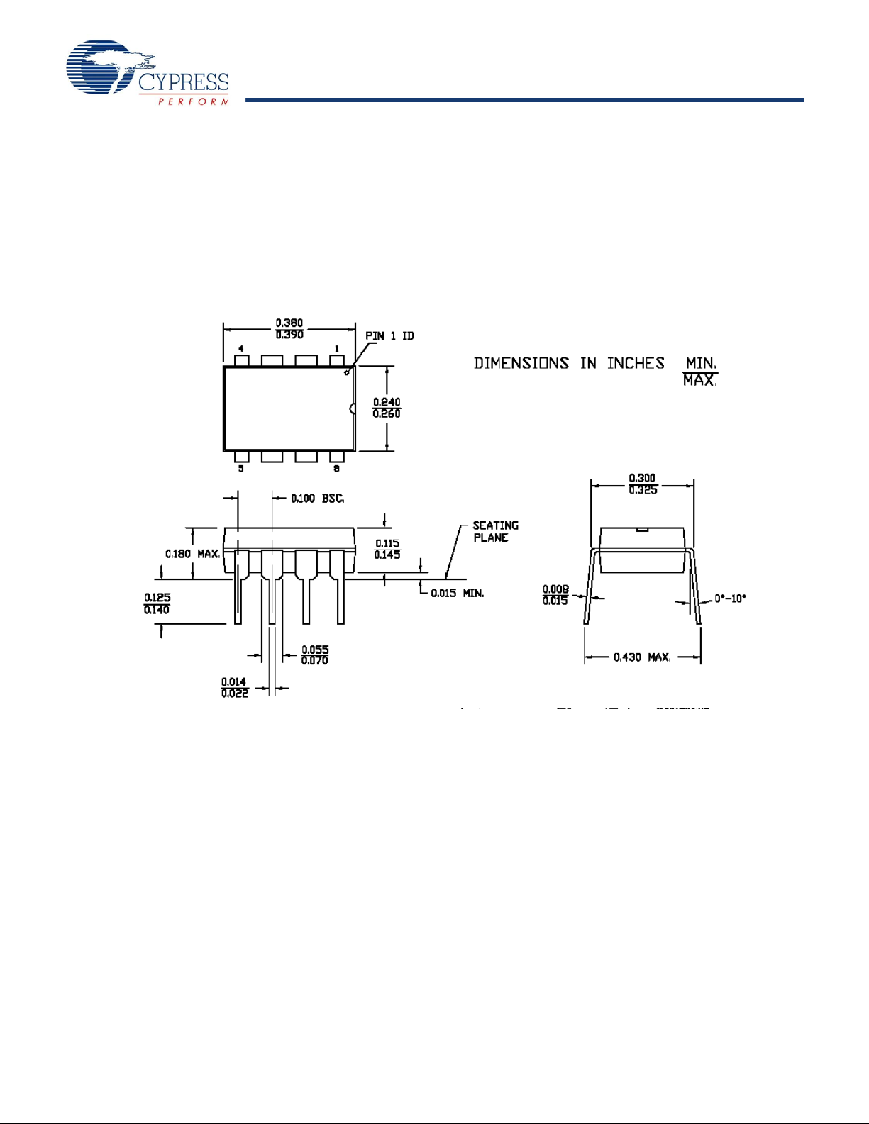
CY8C27143, CY8C27243
CY8C27443, CY8C27543, CY8C27643
Packaging Information
51-85075 *A
This section illustrates the packaging specifications for the CY8C27x4 3 PSoC device, along with the thermal impedan ces for each
package and the typical package capacitance on crystal pins.
Important Note Emulation tools may require a larger area on the target PCB than th e chip’s footprint. For a de tailed description of
the emulation tools’ dimensions, refer to the document titled PSoC Emulator Pod Dimensions at
http://www.cypress.com/design/MR10161.
Packaging Dimensions
Figure 21. 8-Pin (300-Mil) PDIP
Document Number: 38-12012 Rev. *O Page 41 of 53
[+] Feedback
Page 42

CY8C27143, CY8C27243
CY8C27443, CY8C27543, CY8C27643
Figure 22. 20-Pin (210-Mil) SSOP
51-85077 *C
51-85024 *C
Figure 23. 20-Pin (300-Mil) Molded SOIC
Document Number: 38-12012 Rev. *O Page 42 of 53
[+] Feedback
Page 43

CY8C27143, CY8C27243
CY8C27443, CY8C27543, CY8C27643
Figure 24. 28-Pin (300-Mil) Molded DIP
DIMENSIONS IN INCHES [MM]
MIN.
MAX.
SEATING PLANE
0.260[6.60]
0.295[7.49]
0.090[2.28]
0.110[2.79]
0.055[1.39]
0.065[1.65]
0.015[0.38]
0.020[0.50]
0.015[0.38]
0.060[1.52]
0.120[3.05]
0.140[3.55]
0.009[0.23]
0.012[0.30]
0.310[7.87]
0.385[9.78]
0.290[7.36]
0.325[8.25]
0.030[0.76]
0.080[2.03]
0.115[2.92]
0.160[4.06]
0.140[3.55]
0.190[4.82]
1.345[34.16]
1.385[35.18]
3° MIN.
114
15 28
REFERENCE JEDEC MO-095
PART #
P28.3 STANDARD PKG.
LEAD FREE PKG.PZ28.3
LEAD END OPTION
SEE LEAD END OPTION
SEE LEAD END OPTION
(LEAD #1, 14, 15 & 28)
PACKAGE WEIGHT: 2.15gms
51-85014 *E
51-85079 *C
Figure 25. 28-Pin (210-Mil) SSOP
Document Number: 38-12012 Rev. *O Page 43 of 53
[+] Feedback
Page 44

CY8C27143, CY8C27243
CY8C27443, CY8C27543, CY8C27643
Figure 26. 28-Pin (300-Mil) Molded SOIC
51-85026 *D
51-85064 *C
Figure 27. 44-Pin TQFP
Document Number: 38-12012 Rev. *O Page 44 of 53
[+] Feedback
Page 45

CY8C27143, CY8C27243
CY8C27443, CY8C27543, CY8C27643
Figure 28. 48-Pin (300-Mil) SSOP
51-85061-C
51-85061 *C
001-13191 *D
Figure 29. 48-Pin QFN 7x7x 0.90 MM (Sawn Type)
Document Number: 38-12012 Rev. *O Page 45 of 53
[+] Feedback
Page 46

CY8C27143, CY8C27243
CY8C27443, CY8C27543, CY8C27643
Figure 30. 48-Pin (7x7 mm) QFN
51-85152 *C
Important Note For information on the preferred dimensions for mounting QFN packages, see the following Application Note at
http://www.amkor.com/products/notes_papers/MLFAppNote.pdf.
Thermal Impedances Capacitance on Crystal Pins
Table 43. Thermal Impedances per Package
Package Typical θ
8 PDIP 120 oC/W
20 SSOP 116 oC/W
20 SOIC 79 oC/W
28 PDIP 67 oC/W
28 SSOP 95 oC/W
28 SOIC 68 oC/W
44 TQFP 61 oC/W
48 SSOP 69 oC/W
48 QFN 18 oC/W
* TJ = TA + POWER x
θ
JA
JA
*
Table 44. Typical Package Capacitance on Crystal Pins
Package Package Capacitance
8 PDIP 2.8 pF
20 SSOP 2.6 pF
20 SOIC 2.5 pF
28 PDIP 3.5 pF
28 SSOP 2.8 pF
28 SOIC 2.7 pF
44 TQFP 2.6 pF
48 SSOP 3.3 pF
48 QFN 2.3 pF
Document Number: 38-12012 Rev. *O Page 46 of 53
[+] Feedback
Page 47

CY8C27143, CY8C27243
CY8C27443, CY8C27543, CY8C27643
Solder Reflow Peak Temperature
Following is the minimum solder reflow peak temperature to achieve good solderability.
Table 45. Solder Reflow Peak Temperature
Silicon A* Silicon B*
Package
8 PDIP 220oC 240oC 240oC 260oC
20 SSOP 220oC 240oC 240oC 260oC
20 SOIC 220oC 240oC 220oC 260oC
28 PDIP 220oC 240oC 240oC 260oC
28 SSOP 220oC 240oC 240oC 260oC
28 SOIC 220oC 240oC 220oC 260oC
44 TQFP 220oC 240oC 220oC 260oC
48 SSOP 220oC 240oC 220oC 260oC
48 QFN 220oC 240oC 240oC 260oC
*Refer to Table 47 on page 50.
**Higher temperatures may be required based on the solder melting point. Typical temperatures for solder are 220
with Sn-Pb or 245
Minimum Peak
Temperature**
±
5oC with Sn-Ag-Cu paste. Refer to the solder manufacturer specifications.
Maximum Peak
T emperature
Minimum Peak
T emperature*
Maximum Peak
T emperature
±
5oC
Document Number: 38-12012 Rev. *O Page 47 of 53
[+] Feedback
Page 48

CY8C27143, CY8C27243
CY8C27443, CY8C27543, CY8C27643
Development Tool Selection
This chapter presents the development tools available for all
current PSoC device families including the CY8C27x43 family.
Software
PSoC Designer
At the core of the PSoC development software suite is PSoC
Designer, used to generate PSoC firmware applications. PSoC
Designer is available free of charge at
http://www.cypress.com/psocdesigner and includes a free C
compiler.
PSoC Programmer
Flexible enough to be used on the bench in development, yet
suitable for factory programming, PSoC Programmer works
either as a standalone programming application or it can operate
directly from PSoC Designer or PSoC Express. PSoC
Programmer software is compatible with both PSoC ICE-Cube
In-Circuit Emulator and PSoC MiniProg. PSoC programmer is
available free ofcharge at http://www.cypress.com/psocpro-
grammer.
Development Kits
All development kits can be purchased from the Cypress Online
Store.
CY3215-DK Basic Development Kit
The CY3215-DK is for prototyping and development with PSoC
Designer. This kit supports in-circuit emulation and the software
interface allows users to run, halt, and single step the processor
and view the content of specific memory locations. Advance
emulation features also supported through PSoC Designer. The
kit includes:
■
PSoC Designer Software CD
■
ICE-Cube In-Circuit Emulator
■
ICE Flex-Pod for CY8C29x66 Family
■
Cat-5 Adapter
■
Mini-Eval Programming Board
■
110 ~ 240V Power Supply, Euro-Plug Adapter
■
iMAGEcraft C Compiler (Registration Required)
■
ISSP Cable
■
USB 2.0 Cable and Blue Cat-5 Cable
■
2 CY8C29466-24PXI 28-PDIP Chip Samples
™
Evaluation Tools
All evaluation tools can be purchased from the Cypress Online
Store.
CY3210-MiniProg1
The CY3210-MiniProg1 kit allows a user to program PSoC
devices via the MiniProg1 programming unit. The MiniProg is a
small, compact prototyping programmer that connects to the PC
via a provided USB 2.0 cable. The kit includes:
■
MiniProg Programming Unit
■
MiniEval Socket Programming and Evaluation Board
■
28-Pin CY8C29466-24PXI PDIP PSoC Device Sample
■
28-Pin CY8C27443-24PXI PDIP PSoC Device Sample
■
PSoC Designer Software CD
■
Getting Started Guide
■
USB 2.0 Cable
CY3210-PSoCEval1
The CY3210-PSoCEval1 kit features an evaluation board and
the MiniProg1 programming unit. The evaluation board includes
an LCD module, potentiometer, LEDs, and plenty of breadboarding space to meet all of your evaluation needs. The kit
includes:
■
Evaluation Board with LCD Module
■
MiniProg Programming Unit
■
28-Pin CY8C29466-24PXI PDIP PSoC Device Sample (2)
■
PSoC Designer Software CD
■
Getting Started Guide
■
USB 2.0 Cable
CY3214-PSoCEvalUSB
The CY3214-PSoCEvalUSB evaluation kit features a development board for the CY8C24794-24LFXI PSoC device. Special
features of the board include both USB and capacitive sensing
development and debugging support. This evaluation board also
includes an LCD module, potentiometer, LEDs, an enunciator
and plenty of bread boarding space to meet all of your evaluation
needs. The kit includes:
■
PSoCEvalUSB Board
■
LCD Module
■
MIniProg Programming Unit
■
Mini USB Cable
■
PSoC Designer and Example Projects CD
■
Getting Started Guide
■
Wire Pack
Document Number: 38-12012 Rev. *O Page 48 of 53
[+] Feedback
Page 49

CY8C27143, CY8C27243
CY8C27443, CY8C27543, CY8C27643
Device Programmers
Notes
23.Flex-Pod kit includes a practice flex-pod and a practice PCB, in addition to two flex-pods.
24.Foot kit includes surface mount feet that can be soldered to the target PCB.
25.Programming adapter converts non-DIP package to DIP footprint. Specific details and ordering informati on fo r each of the ada pters can be foun d at http://www.em-
ulation.com.
All device programmers can be purchased from the Cypress
Online Store.
CY3207ISSP In-System Serial Programmer (ISSP)
The CY3207ISSP is a production programmer. It includes
protection circuitry and an industrial case that is more robust than
the MiniProg in a production-programming environment.
CY3216 Modular Programmer
The CY3216 Modular Programmer kit features a modular
programmer and the MiniProg1 programming unit. The modular
programmer includes three programming module cards and
supports multiple Cypress products. The kit includes:
■
Modular Programmer Base
■
3 Programming Module Cards
■
MiniProg Programming Unit
■
PSoC Designer Software CD
■
Getting Started Guide
■
USB 2.0 Cable
Note: CY3207ISSP needs special software and is not
compatible with PSoC Programmer. The kit includes:
■
CY3207 Programmer Unit
■
PSoC ISSP Software CD
■
110 ~ 240V Power Supply, Euro-Plug Adapter
■
USB 2.0 Cable
Accessories (Emulation and Programming)
Table 46. Emulation and Programming Accessories
Part # Pin Package Flex-Pod Kit
[23]
Foot Kit
CY8C27143-24PXI 8 PDIP CY3250-27XXX CY3250-8PDIP-FK Adapters can be found at
CY8C27243-24PVXI 20 SSOP CY3250-27XXX CY3250-20SSOP-FK
CY8C27243-24SXI 20 SOIC CY3250-27XXX CY3250-20SOIC-FK
CY8C27443-24PXI 28 PDIP CY3250-27XXX CY3250-28PDIP-FK
CY8C27443-24PVXI 28 SSOP CY3250-27XXX CY3250-28SSOP-FK
CY8C27443-24SXI 28 SOIC CY3250-27XXX CY3250-28SOIC-FK
CY8C27543-24AXI 44 TQFP CY3250-27XXX CY3250-44TQFP-FK
CY8C27643-24PVXI 48 SSOP CY3250-27XXX CY3250-48SSOP-FK
CY8C27643-24LFXI 48 QFN CY3250-2 7XXXQFN CY3250-48QFN-FK
[24]
Adapter
[25]
http://www.emulation.com.
Third-Party Tools
Several tools have been specially designed by the following
3rd-party vendors to accompany PSoC devices during development and production. Specific details for each of these tools
can be found at http://www.cypress.com under DESIGN
RESOURCES >> Evaluation Boards.
Document Number: 38-12012 Rev. *O Page 49 of 53
Build a PSoC Emulator into Your Board
For details on how to emulate your circuit before going to volume
production using an on-chip debug (OCD) non-production PSoC
device, see Application Note “Debugging - Build a PSoC
Emulator into Your Board - AN2323” at
http://www.cypress.com/an2323.
[+] Feedback
Page 50

CY8C27143, CY8C27243
CY8C27443, CY8C27543, CY8C27643
Ordering Information
Note
26.This part may be used for in-circuit debugging. It is NOT available for production.
The following table lists the CY8C27x43 PSoC device’s key package features and ordering codes.
Table 47. CY8C27x43 PSoC Device Key Features and Ordering Information
Package
CY8C27x43 Silicon B – These parts are lead free and offer the f ollowin g improvements. The DEC_CR1 register selections are enhanced to allow any digital block to be
the decimator clock source, the ECO EX and ECO EXW bits in the CPU_SCR1 register are readable, and the accuracy of the analog reference is enhanced (see the
Electrical Specifications chapter). All silicon A errata are fixed in silicon B.
8 Pin (300 Mil) DIP CY8C27143-24PXI 16K 256 No -40C to +85C 8 12 6 4 4 No
20 Pin (210 Mil) SSOP CY8C27243-24PVXI 16K 256 Yes -40C to +85C 8 12 16 8 4 Yes
20 Pin (210 Mil) SSOP
(Tape and Reel)
20 Pin (300 Mil) SOIC CY8C27243-24SXI 16K 256 Yes -40C to +85C 8 12 16 8 4 Yes
20 Pin 300 Mil) SOIC
(Tape and Reel)
28 Pin (300 Mil) DIP CY8C27443-24PXI 16K 256 Yes -40C to +85C 8 12 24 12 4 Yes
28 Pin (210 Mil) SSOP CY8C27443-24PVXI 16K 256 Yes -40C to +85C 8 12 24 12 4 Yes
28 Pin (210 Mil) SSOP
(Tape and Reel)
28 Pin (300 Mil) SOIC CY8C27443-24SXI 16K 256 Yes -40C to +85C 8 12 24 12 4 Yes
28 Pin (300 Mil) SOIC
(Tape and Reel)
44 Pin TQFP CY8C27543-24AXI 16K 256 Yes -40C to +85C 8 12 40 12 4 Yes
44 Pin TQFP
(Tape and Reel)
48 Pin (300 Mil) SSOP CY8C27643-24PVXI 16K 256 Yes -40C to +85C 8 12 44 12 4 Yes
48 Pin (300 Mil) SSOP
(Tape and Reel)
48 Pin (7x7) QFN CY8C27643-24LFXI 16K 256 Yes -40C to +85C 8 12 44 12 4 Yes
48 Pin (7x7) QFN
(Tape and Reel)
48 Pin (7X7X 0.90 MM) QFN (Sawn) CY8C27643-24LTXI 16K 256 Yes -40C to +85C 8 12 44 12 4 Yes
48 Pin (7X7X 0.90 MM) QFN (Sawn) CY8C27643-24LTXIT 16K 256 Yes -40C to +85C 8 12 44 12 4 Yes
56 Pin OCD SSOP CY8C27002-24PVXI
CY8C27x43 Silicon A – Silicon A is not recommended for new designs.
8 Pin (300 Mil) DIP CY8C27143-24PI 16K 256 No -40C to +85C 8 12 6 4 4 No
20 Pin (210 Mil) SSOP CY8C27243-24PVI 16K 256 Yes -40C to +85C 8 12 16 8 4 Yes
20 Pin (210 Mil) SSOP
(Tape and Reel)
20 Pin (300 Mil) SOIC CY8C27243-24SI 16K 256 Yes -40C to +85C 8 12 16 8 4 Yes
20 Pin 300 Mil) SOIC
(Tape and Reel)
28 Pin (300 Mil) DIP CY8C27443-24PI 16K 256 Yes -40C to +85C 8 12 24 12 4 Yes
28 Pin (210 Mil) SSOP CY8C27443-24PVI 16K 256 Yes -40C to +85C 8 12 24 12 4 Yes
28 Pin (210 Mil) SSOP
(Tape and Reel)
28 Pin (300 Mil) SOIC CY8C27443-24SI 16K 256 Yes -40C to +85C 8 12 24 12 4 Yes
28 Pin (300 Mil) SOIC
(Tape and Reel)
44 Pin TQFP CY8C27543-24AI 16K 256 Yes -40C to +85C 8 12 40 12 4 Yes
CY8C27243-24PVXIT 16K 256 Yes -40C to +85C 8 12 16 8 4 Yes
CY8C27243-24SXIT 16K 256 Yes -40C to +85C 8 12 16 8 4 Yes
CY8C27443-24PVXIT 16K 256 Yes -40C to +85C 8 12 24 12 4 Yes
CY8C27443-24SXIT 16K 256 Yes -40C to +85C 8 12 24 12 4 Yes
CY8C27543-24AXIT 16K 256 Yes -40C to +85C 8 12 40 12 4 Yes
CY8C27643-24PVXIT 16K 256 Yes -40C to +85C 8 12 44 12 4 Yes
CY8C27643-24LFXIT 16K 256 Yes -40C to +85C 8 12 44 12 4 Yes
CY8C27243-24PVIT 16K 256 Yes -40C to +85C 8 12 16 8 4 Yes
CY8C27243-24SIT 16K 256 Yes -40C to +85C 8 12 16 8 4 Yes
CY8C27443-24PVIT 16K 256 Yes -40C to +85C 8 12 24 12 4 Yes
CY8C27443-24SIT 16K 256 Yes -40C to +85C 8 12 24 12 4 Yes
Ordering
Code
[26]
16K 256 Yes -40C to +85C 8 12 44 14 4 Yes
RAM
Flash
(Bytes)
Pump
(Bytes)
Switch Mode
Range
Temperature
(Rows of 4)
Digital Blocks
Analog Blocks
Pins
Inputs
Analog
Analog
Outputs
Digital I/O
(Columns of 3)
XRES Pin
Document Number: 38-12012 Rev. *O Page 50 of 53
[+] Feedback
Page 51

CY8C27143, CY8C27243
CY8C27443, CY8C27543, CY8C27643
Table 47. CY8C27x43 PSoC Device Key Features and Ordering Information (contin ued)
CY 8 C 27 xxx-24xx
Package Type: Thermal Rating:
PX = PDIP Pb-Free C = Commercial
SX = SOIC Pb-Free I = Industrial
PVX = SSOP Pb-Free E = Extended
LFX/LKX = QFN Pb-Free
AX = TQFP Pb-Free
Speed: 24 MHz
Part Number
Family Code
Technology Code: C = CMOS
Marketing Code: 8 = Cypress PSoC
Company ID: CY = Cypress
Package
44 Pin TQFP
(Tape and Reel)
48 Pin (300 Mil) SSOP CY8C27643-24PVI 16K 256 Yes -40C to +85C 8 12 44 12 4 Yes
48 Pin (300 Mil) SSOP
(Tape and Reel)
48 Pin (7x7) MLF CY8C27643-24LFI 16K 256 Yes -40C to +85C 8 12 44 12 4 Yes
48 Pin (7x7) MLF
(Tape and Reel)
48 Pin (7X7X 0.90 MM) QFN (Sawn) CY8C27643-24LTXI 16K 256 Yes -40C to +85C 8 12 44 12 4 Yes
48 Pin (7X7X 0.90 MM) QFN (Sawn) CY8C27643-24LTXIT 16K 256 Yes -40C to +85C 8 12 44 12 4 Yes
CY8C27543-24AIT 16K 256 Yes -40C to +85C 8 12 40 12 4 Yes
CY8C27643-24PVIT 16K 256 Yes -40C to +85C 8 12 44 12 4 Yes
CY8C27643-24LFIT 16K 256 Yes -40C to +85C 8 12 44 12 4 Yes
Ordering
Code
Flash
RAM
(Bytes)
Pump
(Bytes)
Switch Mode
Range
Temperature
(Rows of 4)
Digital Blocks
Analog Blocks
Pins
Inputs
Analog
Analog
Digital I/O
(Columns of 3)
Outputs
Note For Die sales information, contact a local Cypress sales office or Field Applications Engineer (FAE).
Ordering Code Definitions
XRES Pin
Document Number: 38-12012 Rev. *O Page 51 of 53
[+] Feedback
Page 52

CY8C27143, CY8C27243
CY8C27443, CY8C27543, CY8C27643
Document History Page
Document Title: CY8C27143, CY8C27243, CY8C27443, CY8C27543, CY8C27643 PSoC® Programmable System-on-Chip
Document Number: 38-12012
Revision ECN No.
Submission
Date
** 127087 7/01/2003 New Silicon. New document (Revision **).
*A 128780 7/29/2003 Engineering and
*B 128992 8/14/2003 NWJ Interrupt controller table fixed, refinements to Electrical Spec section and
*C 129283 8/28/2003 NWJ Significant changes to the Electrical Specifications section.
*D 129442 9/09/2003 NWJ Changes made to Electrical Spec section. Added 20/28-Lead SOIC
*E 130129 10/13/2003 NWJ Revised document for Silicon Revision A.
*F 130651 10/28/2003 NWJ Refinements to Electrical Specification section and I2C chapter.
*G 131298 11/18/2003 NWJ Revisions to GDI, RDI, and Digital Block chapters. Revisions to AC Digital
*H 229416 See ECN SFV New data sheet format and organization. Reference the PSoC Program-
*I 247529 See ECN SFV Added Silicon B information to this data sheet.
*J 355555 See ECN HMT Add DS standards, update device table, swap 48-pin SSOP 45 and 46, add
*K 523233 See ECN HMT Add Low Power Comparator (LPC) AC/DC electrical spec. tables. Add new
*L 2545030 07/29/2008 YARA Added note to DC Analog Reference Specification table and Ordering Infor-
*M 2696188 04/22/2009 DPT/PYRS Changed title from “ CY8C27143, CY8C27243, CY8C27443, CY8C27543,
*N 2762501 09/11/2009 MAXK Updated DC GPIO, AC Chip-Level, and AC Programming Specifications as
*O 2811860 11/20/2009 ECU Added Contents page. In the Ordering Information table, added 48 Sawn
NWJ.
Origin of
Change
Description of Change
New electrical spec additions, fix of Core Architecture links, corrections to
some text, tables, drawings, and format.
Register chapter.
packages and pinouts.
Block Spec and miscellaneous register changes.
mable System-on-Chip Technical Reference Manual for additional information. Title change.
Reflow Peak Temp. table. Add new color and logo. Re-add pinout ISSP
notation. Add URL to preferred dimensions for mounting MLF packages.
Update Transmitter and Receiver AC Digital Block Electrical Specifications.
Dev. Tool section. Add CY8C20x34 to PSoC Device Characteristics table.
Add OCD pinout and package diagram. Add ISSP note to pinout tables.
Update package diagram revisions. Update typical and recommended
Storage Temperature per industrial specs. Update CY branding and QFN
convention. Update copyright and trademarks.
mation.
and CY8C27643 PSoC Mixed Signal Array Final Data Sheet” to
“CY8C27143, CY8C27243, CY8C27443, CY8C27543, CY8C27643
PSoC® Programmable System-on-Chip™”. Updated data sheet template.
Added 48-Pin QFN (Sawn) package outline diagram and Ordering information details for CY8C27643-24LTXI and CY8C27643-24LTXIT parts
follows:
Modified T
Replaced T
cation.
specification.
WRITE
(time) specification with SR
RAMP
POWER_UP
(slew rate) specifi-
Added note [9] to Flash Endurance specification.
Added IOH, IOL, DCILO, F32K_U, T
and T
PROGRAM_COLD
specifications.
POWERUP
, T
ERASEALL
, T
PROGRAM_HOT
QFN (LTXI) to the Silicon B parts. Updated 28-Pin package drawing
(51-85014)
,
Document Number: 38-12012 Rev. *O Page 52 of 53
[+] Feedback
Page 53

CY8C27143, CY8C27243
CY8C27443, CY8C27543, CY8C27643
Sales, Solutions, and Legal Information
Worldwide Sales and Design Support
Cypress maintains a worldwide network of offices, solution centers, manufacturer’s representatives, and distributors. T o find the office
closest to you, visit us at cypress.com/sales.
Products
PSoC psoc.cypress.com
Clocks & Buffers clocks.cypress.com
Wireless wireless.cypress.com
Memories memory.cypress.com
Image Sensors image.cypress.com
© Cypress Semiconductor Corporation, 2003-2009. The information contained herein is subject to change without notice. Cypress Semiconductor Corporation assumes no responsibility for the use
of any circuitry other than circuit ry e mbod ied in a Cyp ress produc t. Nor does it conve y or im ply any lic ense under paten t or ot her ri ghts. Cypr ess pr oducts are not wa rrante d nor inte nde d to be use d
for medical, life support, life saving, criti cal co ntr ol or safety applications, unless pursuant to an express written agreement with Cypress. Furthermore, Cypress does not authorize its products for use
as critical components in life-support systems where a malfunction or failure may reasonably be expected to result in significant injury to the user. The inclusion of Cypress products in life-support
systems application implies that the manufacturer assumes all risk of such use and in doing so indemnifies Cypress against all charges.
Any Source Code (software and/or firmware) is owned by Cypress Semiconductor Corporation (Cypress) and is protected by and subject to worldwide patent protection (United States and foreign),
United States copyrigh t laws and interna tional tr eaty pr ovision s. Cypr ess here by gra nt s to lic ensee a p erson al, no n-excl usive , non- tran sferabl e license to copy, use, modify , cr eate d erivati ve works of ,
and compile the Cypress Source Code and derivative works for the sole purpose of creating custom software and or firmware in support of licensee product to be used only in conju nction with a Cypress
integrated circuit as specified in the ap plicable agr eement. Any reprod uction, modificati on, translation, co mpilation, or re presentatio n of this Source Code except as spe cified above is prohibited wi thout
the express written permission of Cypress.
Disclaimer: CYPRESS MAKES NO WARRANTY OF ANY KIND, EXPRESS OR IMPLIED, WITH REGARD TO THIS MATERIAL, INCLUDING, BUT NOT LIMITED TO, THE IMPLIED WARRANTIES
OF MERCHANTABILITY AND FITNESS FOR A PARTICULAR PURPOSE. Cypress reserves the right to make changes without further notice to the materials described herein. Cypress does not
assume any liability arising out of the app licati on or us e of an y product or circ uit de scrib ed herei n. Cypr ess does n ot auth orize it s product s for use a s critical component s in life-suppo rt systems where
a malfunction or failure may reasonably be expected to result in significant injury to the user. The inclusion of Cypress’ product in a life-support systems application implies that the manufacturer
assumes all risk of such use and in doing so indemnifies Cypress against all charges.
Use may be limited by and subject to the applicable Cypress software license agreement.
Document Number: 38-12012 Rev. *O Revised November 20, 2009 Page 53 of 53
PSoC Designer™ is a trademark a nd PSoC® is a r egistered tradema rk of C ypress Se miconducto r Cor p. All other tra demarks or regi stered trade marks referenced herein are proper ty of the respective
corporations. Purchase of I 2C comp onents from C ypres s or on e of its sublice nsed A sso ciate d Companies conve ys a licens e unde r th e Philips I2C Patent Rights to use these components in an I2C
system, provided that the system conforms to the I2C Standard Specification as defined by Philips.
[+] Feedback
 Loading...