

Datasheet CY8C20110, CY8C20180, CY8C20160, CY8C20140, CY8C20142 Datasheet (Cypress Semiconductor)
Page 1

CY8C20110/CY8C20180/CY8C20160
CY8C20140/CY8C20142
CapSense® Express™ Button
Capacitive Controllers
Features
■
10/8/6/4 Capacitive Button Input
❐
Robust sensing algorithm
❐
High sensitivity, low noise
❐
Immunity to RF and AC noise
❐
Low radiated EMC noise
❐
Supports wide range of input capacitance, sensor shapes,
and sizes
■
Target Applications
❐
Printers
❐
Cellular handsets
❐
LCD monitors
❐
Portable DVD players
■
Low Operating Current
❐
Active current: continuous sensor scan: 1.5 mA
❐
Deep sleep current: 4 uA
■
Industry's Best Configurability
❐
Custom sensor tuning, one optional capacitor
❐
Output supports strong drive for LED
❐
Output state can be controlled through I2C or directly from
CapSense® input state
❐
Run time re-configurable over I2C
■
Advanced Features
❐
All GPIOs support LED dimming with configurable delay
option in CY8C21110
❐
Interrupt outputs
❐
User defined Inputs
❐
Wake on interrupt input
❐
Sleep control pin
❐
Nonvolatile storage of custom settings
❐
Easy integration into existing products – configure output to
match system
❐
No external components required
❐
World class free configuration tool
■
Wide Range of Operating Voltages
❐
2.4V to 2.9V
❐
3.10V to 3.6V
❐
4.75V to 5.25V
■
I2C Communication
❐
Supported from 1.8V
❐
Internal pull up resistor support option
❐
Data rate up to 400 kbps
❐
Configurable I2C addressing
■
Industrial temperature range: –40°C to +85°C.
■
Available in16-pin COL, 8-pin, and 16-pin SOIC Packages
Overview
These CapSense Express™ controllers support 4 to 10 capacitive sensing (CapSense buttons). The device functionality is
configured through an I2C port and can be stored in onboard
nonvolatile memory for automatic loading at power on. The
CY8C20110 is optimized for dimming LEDs in 15 selectable duty
cycles for back light applications. The device can be configured
to have up to 10 GPIOs connected to the PWM output. The PWM
duty cycle is programmable for variable LED intensities.
The four key blocks that make up these devices are: a robust
capacitive sensing core with high immunity against radiated and
conductive noise, control registers with nonvolatile storage,
configurable outputs, and I
configure registers with parameters needed to adjust the
operation and sensitivity of the CapSense buttons and outputs
and permanently store the settings. The standard I
communication interface enables the host to configure the
device and read sensor information in real time. The I2C address
is fully configurable without any external hardware strapping.
2
C communications. The user can
2
C serial
Cypress Semiconductor Corporation • 198 Champion Court • San Jose,CA 95134-1709 • 408-943-2600
Document Number: 001-54606 Rev. *A Revised December 16, 2009
[+] Feedback
Page 2

CY8C20110/CY8C20180/CY8C20160
CY8C20140/CY8C20142
Contents
Features ..............................................................................1
Overview .............................................................................1
Contents ............................................................................. 2
Pinouts ...............................................................................3
Typical Circuits ..................................................................6
Circuit-1: Five Button and Five LED with I2C Interface 6
Circuit 2 - Two Buttons and Two LEDs
with I2C Interface .........................................................6
Circuit 3 - Compatibility with 1.8V I2C Signaling .........7
Circuit 4 - Powering Down CapSense Express
Device for Low Power Requirements ...........................7
I2C Interface .......................................................................8
I2C Device Addressing .................................................8
I2C Clock Stretching .....................................................8
Format for Register Write and Read ............................9
Operating Modes of I2C Commands ..............................10
Normal Mode ..............................................................10
Setup Mode .............................................................. ..10
Device Operation Modes .................................................10
Active Mode ................................................................10
Periodic Sleep Mode ..................................................10
Deep Sleep Mode .......................................................10
Sleep Control Pin .............................................................10
Interrupt Pin to Master ....................................................10
LED Dimming ...................................................................10
LED Dimming Mode 1: Change Intensity on
ON/OFF Button Status ...............................................11
LED Dimming Mode 2: Flash Intensity on
ON Button Status .......................................................11
LED Dimming Mode 3: Hold Intensity After
ON/OFF Button Transition ..........................................12
LED Dimming Mode 4: Toggle Intensity on
ON/OFF or OFF/ON Button Transitions .....................12
Register Map ............................................................ ........13
CapSense Express Commands ................................17
Register Conventions .................................................17
Layout Guidelines and Best Practices ..........................18
CapSense Button Shapes ..........................................18
Button Layout Design .................................................18
Recommended via Hole Placement ...........................18
Example PCB Layout Design with
Two CapSense Buttons and Two LEDs .....................20
Operating Voltages ..........................................................21
CapSense Constraints ............ ........................................21
Electrical Specifications .................................................22
Absolute Maximum Ratings ........................................22
Operating Temperature ..............................................22
DC Electrical Characteristics .........................................22
DC Chip Level Specifications .....................................22
5V and 3.3V DC General Purpose I/O Specifications 22
2.7 DC General Purpose IO Specifications ................23
2.7V DC Spec for I2C Line with 1.8V
External Pull Up ..........................................................24
DC POR and LVD Specifications ...............................24
DC Flash Write Specifications ....................................25
CapSense Electrical Characteristics ..........................25
AC Electrical Specifications ...........................................26
5V and 3.3V AC General Purpose I/O Specifications 26
2.7V AC General Purpose I/O Specifications .............26
2
C Specifications .................................................26
AC I
Appendix- Examples of Frequently Used
I2C Commands ................................................................27
Ordering Information .......................................................28
Ordering Code Definition ............................................28
Package Diagrams ...........................................................29
Document History Page ............................................ ......31
Sales, Solutions, and Legal Information .......................31
Worldwide Sales and Design Support ........................31
Products .....................................................................31
PSoC Solutions ..........................................................31
Document Number: 001-54606 Rev. *A Page 2 of 31
[+] Feedback
Page 3
CY8C20110/CY8C20180/CY8C20160
CY8C20140/CY8C20142
Pinouts
Note
1. 8/6/4 available configurable IOs can be configured to any of the 10 IOs of the package. Af ter any of the 8/6/4 IOs are ch osen, the remaining 2/ 4/6 IOs of the p ackage
are not available for any functionality.
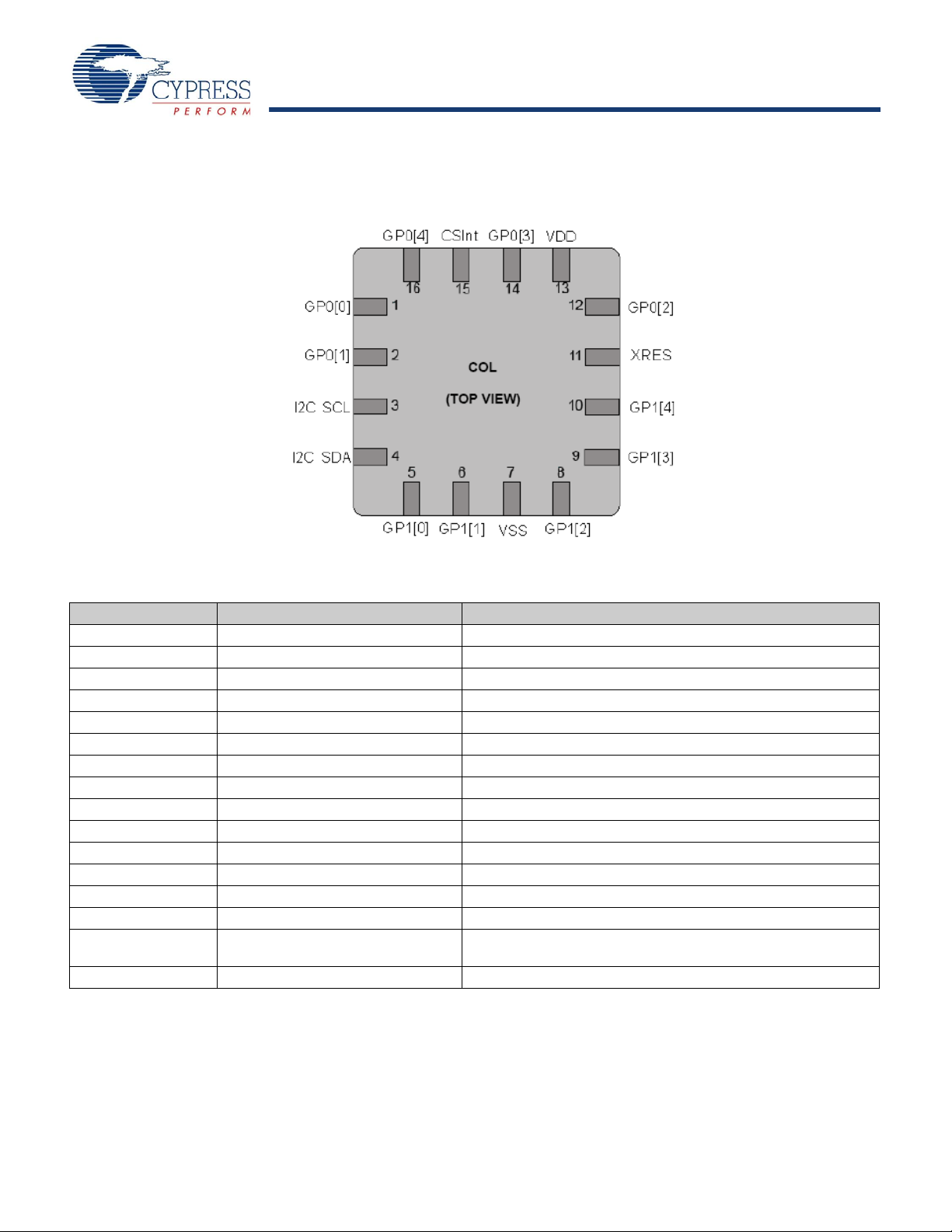
Figure 1. Pin Diagram - 16 COL- CY8C20110 (10 Buttons)/CY8C20180 (8 Buttons)
Table 1. Pin Definitions – 16 COL- CY8C20110 (10 Buttons)/CY8C20180 (8 Buttons)
CY8C20160 (6 Buttons)/CY8C20140 (4 Buttons)
Pin No. Pin Name Description
1 GP0[0] Configurable as CapSense or GPIO
2 GP0[1] Configurable as CapSense or GPIO
3I
4I
5 GP1[0] Configurable as CapSense or GPIO
6 GP1[1] Configurable as CapSense or GPIO
7 VSS Ground Connection
8 GP1[2] Configurable as CapSense or GPIO
9 GP1[3] Configurable as CapSense or GPIO
10 GP1[4] Configurable as CapSense or GPIO
11 XRES Active high external reset with internal pull up
12 GP0[2] Configurable as CapSense or GPIO
13 VDD Supply voltage
14 GP0[3] Configurable as CapSense or GPIO
15 CSInt Integrating Capacitor Input. The external capacitance is required
16 GP0[4] Configurable as CapSense or GPIO
CY8C20160 (6 Buttons)/CY8C20140 (4 Buttons)
[1]
2
C SCL I2C Clock
2
C SDA I2C Data
only if 5:1 SNR cannot be achieved. Typical range is 1 nF to 4.7 nF
Document Number: 001-54606 Rev. *A Page 3 of 31
[+] Feedback
Page 4
CY8C20110/CY8C20180/CY8C20160
CY8C20140/CY8C20142
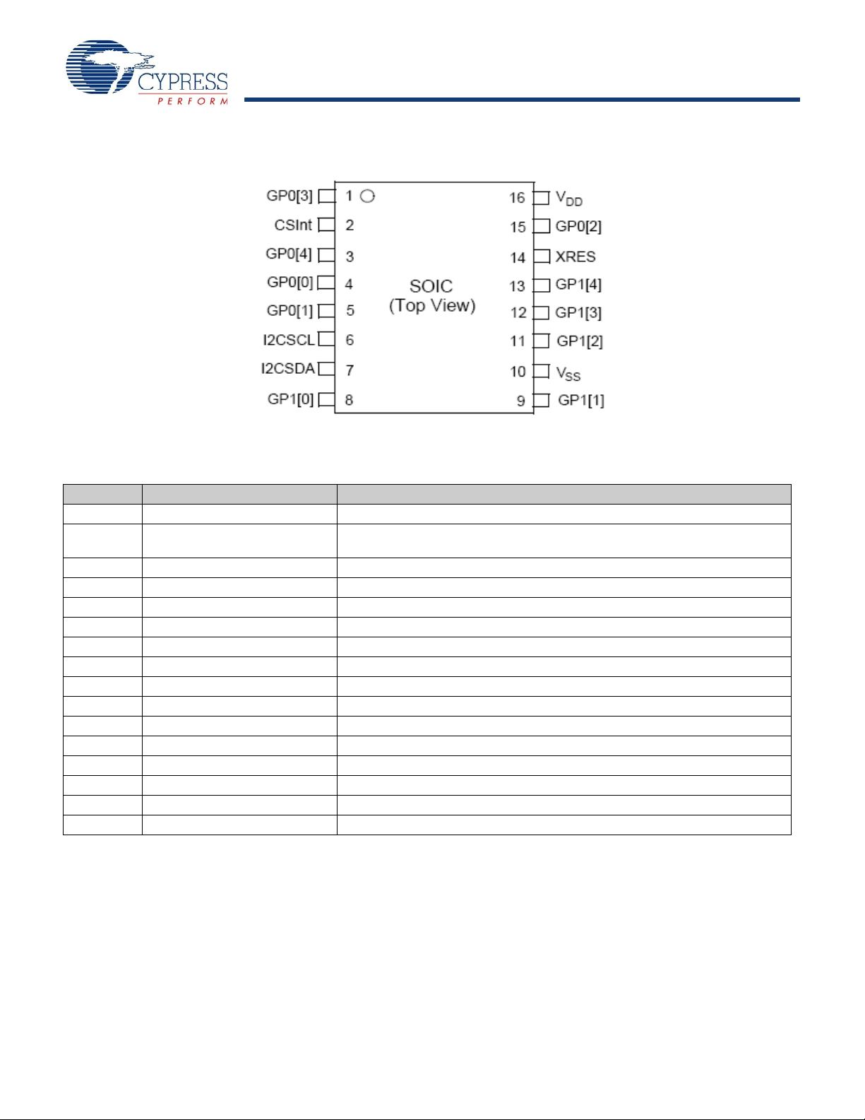
Figure 2. Pin Diagram – 16 SOIC– CY8C20110 (10 Buttons)/CY8C20180 (8 Buttons)
CY8C20160 (6 Buttons)/CY8C20140 (4 Buttons)
Table 2. Pin Definitions – 16 SOIC– CY8C20110 (10 Buttons)/CY8C20180 (8 Buttons)
CY8C20160 (6 Buttons)/CY8C20140 (4 Buttons)
Pin No Name Description
1 GP0[3] Configurable as CapSense or GPIO
2 CSint Integrating Capacitor Input. The external capacitance is required only if 5:1 SNR
3 GP0[4] Configurable as CapSense or GPIO
4 GP0[0] Configurable as CapSense or GPIO
5 GP0[1] Configurable as CapSense or GPIO
6I
7I
8 GP1[0] Configurable as CapSense or GPIO
9 GP1[1] Configurable as CapSense or GPIO
10 VSS Ground Connection
11 GP1[2] Configurable as CapSense or GPIO
12 GP1[3] Configurable as CapSense or GPIO
13 GP1[4] Configurable as CapSense or GPIO
14 XRES Active high external reset with internal pull up
15 GP0[2] Configurable as CapSense or GPIO
16 VDD Supply voltage
2
C SCL I2C Clock
2
C SDA I2C Data
1]
cannot be achieved. Typical range is 1 nF to 4.7 nF
Document Number: 001-54606 Rev. *A Page 4 of 31
[+] Feedback
Page 5
CY8C20110/CY8C20180/CY8C20160
CY8C20140/CY8C20142
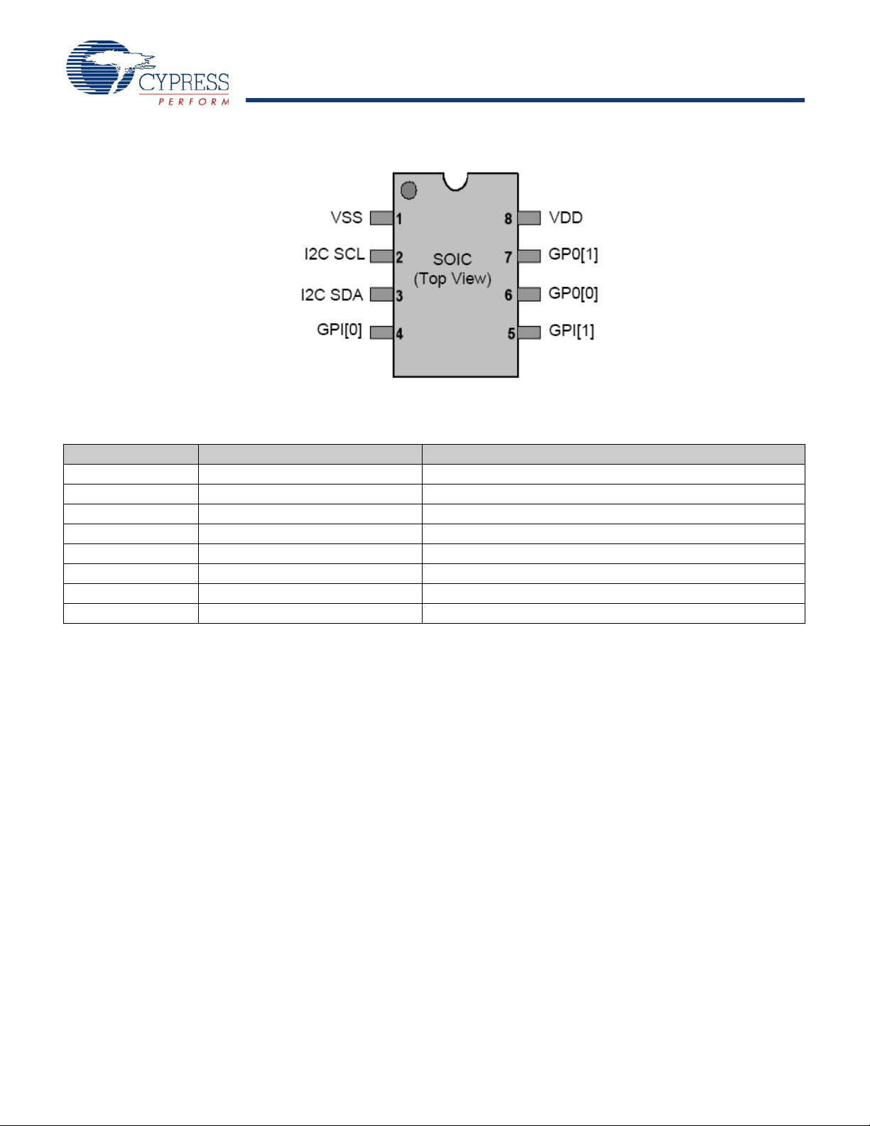
Figure 3. Pin Diagram - 8-Pin SOIC- CY8C20142 (4 Button)
Table 3. Pin Definitions - 8-Pin SOIC - CY8C20142 (4 Button)
Pin No Name Description
1 VSS Ground
2I
3I
4 GP1[0] Configurable as CapSense or GPIO
5 GP1[1] Configurable as CapSense or GPIO
6 GP0[0] Configurable as CapSense or GPIO
7 GP0[1] Configurable as CapSense or GPIO
8 VDD Supply voltage
2
C SCL I2C Clock
2
C SDA I2C Data
Document Number: 001-54606 Rev. *A Page 5 of 31
[+] Feedback
Page 6
CY8C20110/CY8C20180/CY8C20160
CY8C20140/CY8C20142
Typical Circuits
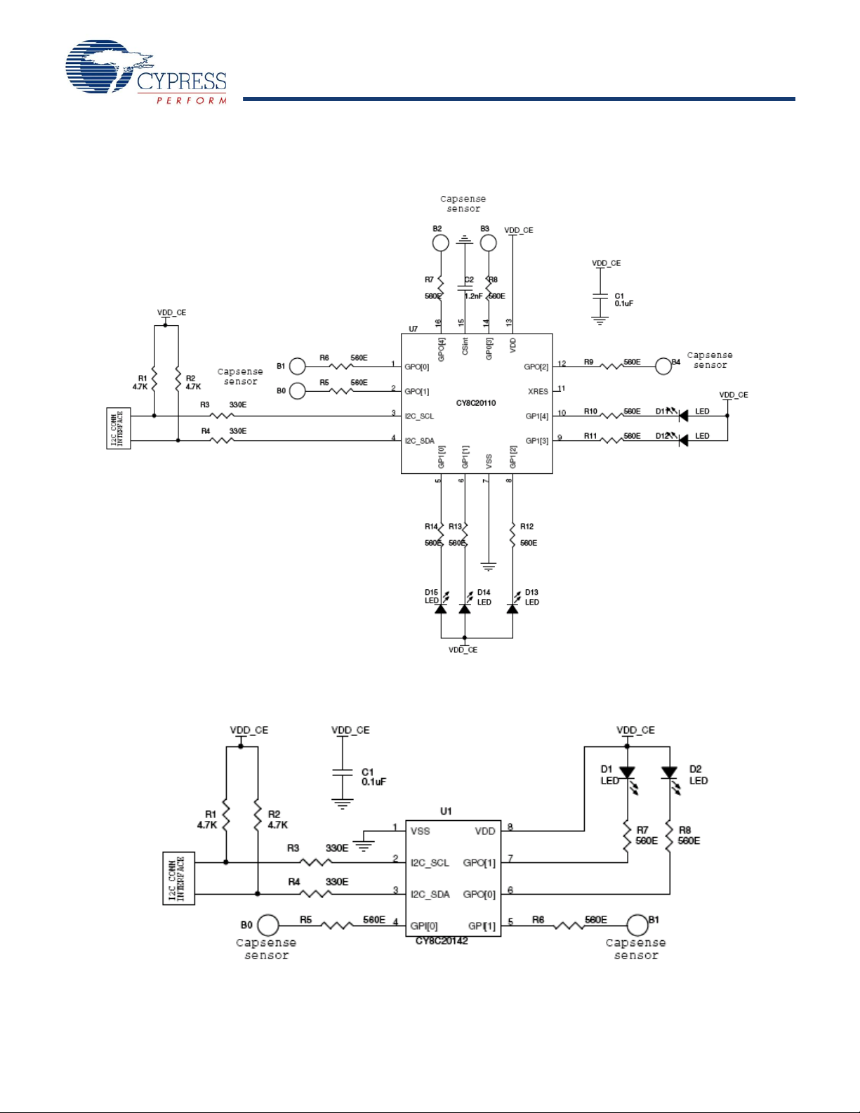
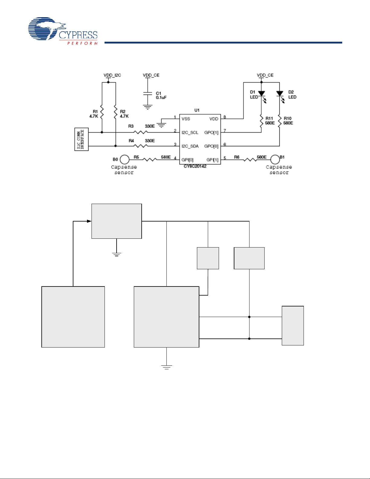
Circuit-1: Five Button and Five LED with I2C Interface
2
Circuit 2 - Two Buttons and Two LEDs with I
C Interface
Document Number: 001-54606 Rev. *A Page 6 of 31
[+] Feedback
Page 7
CY8C20110/CY8C20180/CY8C20160
CY8C20140/CY8C20142
Circuit 3 - Compatibility with 1.8V I2C Signaling
Master
Or
Host
LDO
CapSense Express
I2C Pull
UPs
LED
I2C
BUS
SDA
SCL
VDDOutput
Output
enable
Note 1.8V ≤ VDD_I2C ≤ VDD_CE and 2.4V ≤ VDD_CE ≤ 5.25V
Circuit 4 - Powering Down CapSense Express Device for Low Power Requirements
For low power requirements, if Vdd is to be turned off, this concept can be used. The requirement is that the Vdds of CapSense
Express, I
the device while it is unpowered. The I
pins of the master can cater to the power supply requirements of the circuit, the LDO can be avoided.
2
C pull ups, and LEDs should be from the same source such that turning off the Vdd ensures that no signal is applied to
2
C signals should not be driven high by the master in this situation. If a port pin or group of port
Document Number: 001-54606 Rev. *A Page 7 of 31
[+] Feedback
Page 8

CY8C20110/CY8C20180/CY8C20160
CY8C20140/CY8C20142
I2C Interface
The CapSense Express devices support the industry standard I2C protocol, which can be used for:
■
Configuring the device
■
Reading the status and data registers of the device
■
Controlling device operation
■
Executing commands
2
The I
C address can be modified during configuration.
I2C Device Addressing
The device uses a seven bit addressing protocol. The I2C data transfer is always ini tiated by the master sending a one byte address:
the first 7 bits contain the address and the LSB indicates the data transfer direction. Zero in the LSB bit indicates the write transaction
from master and one indicates read transfer by the master. The following table shows examples for different I
2
Table 4. I
C Address Examples
2
C addresses.
7 Bit Slave
Address
D7 D6 D5 D4 D3 D2 D1 D0 8 Bit Slave Address
1 00000 0 10(W) 02
1 00000 0 11(R) 03
75 10010 1 10(W) 96
75 10010 1 11(W) 97
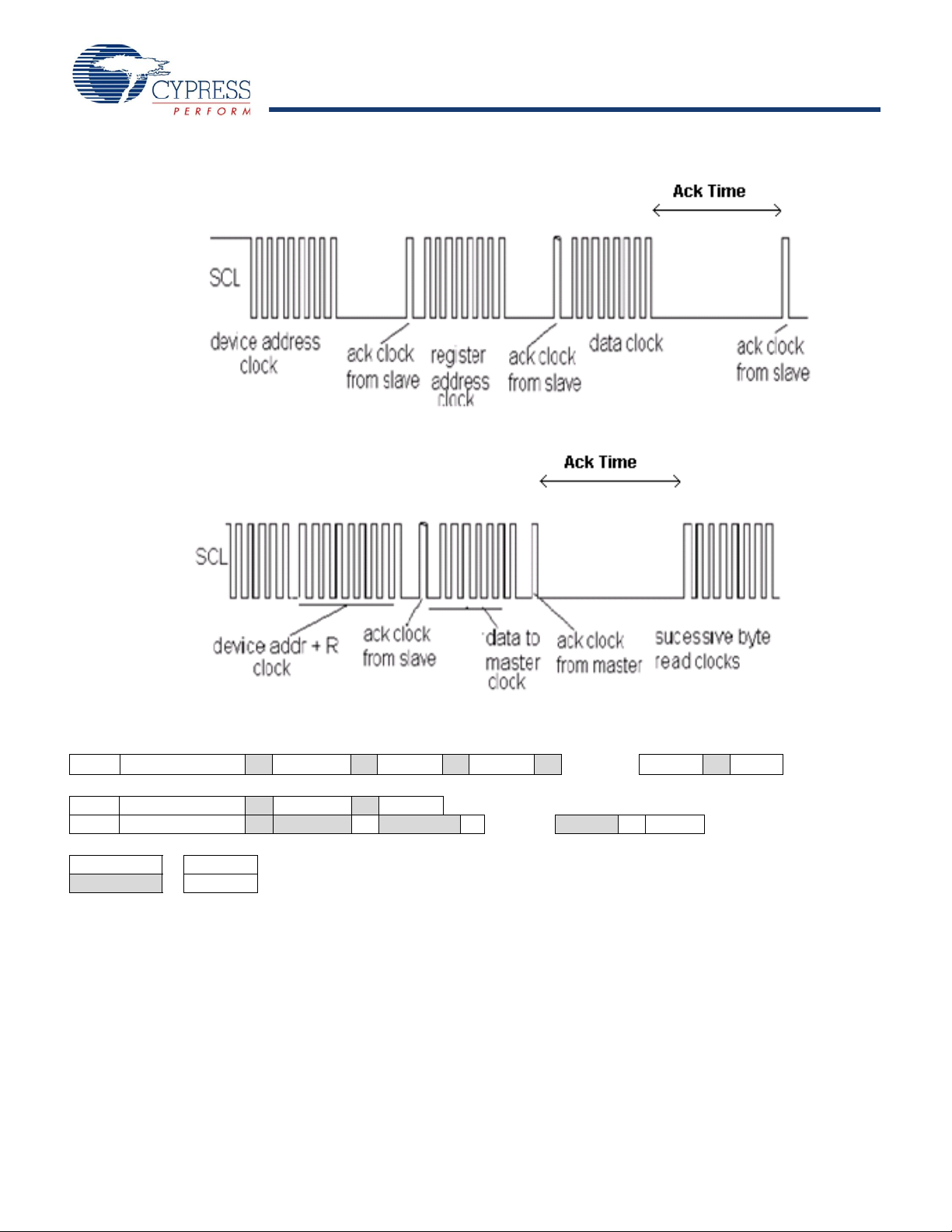
I2C Clock Stretching
‘Clock stretching’ or ‘bus stalling’ in I2C communication protocol
is a state in which the slave holds the SCL line low to indicate
that it is busy. In this condition, the master is expected to wait till
the SCL is released by the slave.
When an I
device, the CapSense Express stalls the I
reception of each byte (that is, just before the ACK/NAK bit) until
processing of the byte is complete and critical internal functions
are executed. Use a fully I
with the CapSense Express device.
2
C master communicates with the CapSense Express
2
C compliant master to communicate
2
C bus after the
If the I2C master does not support clock stretching (a bit banged
software I
2
C Master), the master must wait for a specific amount
of time (as specified in “Format for Register Write and Read” on
page 9) for each register write and read operation before the next
bit is transmitted. The I
should be high) before the I
2
C master must check the SCL status (it
2
C master initiates any data transfer
with CapSense Express. If the master fails to do so and
continues to communicate, the communication is erroneous.
The following diagrams represent the ACK time delays shown in
“Format for Register Write and Read” on page 9 for write and
read.
Document Number: 001-54606 Rev. *A Page 8 of 31
[+] Feedback
Page 9
CY8C20110/CY8C20180/CY8C20160
CY8C20140/CY8C20142
Figure 4. Write ACK Time Representation
Notes
2. Time to process the received data
3. Time taken for the device to send next byte
[2]
Figure 5. Read ACK Time Representation
[3]
Format for Register Write and Read
Register write format
Start Slave Addr + W AReg AddrADataADataA . . . . . Data A Stop
Register read format
Start Slave Addr + W
Start Slave Addr + R
Legends:
Master A - ACK
Slave N- NAK
AReg AddrAStop
A Data A Data A . . . . . Data NStop
Document Number: 001-54606 Rev. *A Page 9 of 31
[+] Feedback
Page 10

CY8C20110/CY8C20180/CY8C20160
CY8C20140/CY8C20142
Operating Modes of I2C Commands
Normal Mode
In normal mode of operation, the acknowledgment time is
optimized. The timings remain approximately the same for
different configurations of the slave. To reduce the acknowledgment times in normal mode, the registers 0x06-0x09, 0x0C,
0x0D, 0x10-0x17, 0x50, 0x51, 0x57-0x60, 0x7E are given only
read access. Write to these registers can be done only in setup
mode.
Setup Mode
All registers have read and write access (except those which are
read only) in this mode. The acknowledgment times are longer
compared to normal mode. When CapSense scanning is
disabled (command code 0x0A in command register 0xA0), the
acknowledgment times can be improved to values similar to the
normal mode of operation.
Device Operation Modes
CapSense Express devices are configured to operate in any of
the following three modes to meet different power consumption
requirements:
■
Active Mode
■
Periodic Sleep Mode
■
Deep Sleep Mode
Active Mode
In the active mode, all the device blocks including the CapSense
sub system are powered. Typical active current consumption of
the device across the operating voltage range is 1.5 mA.
Periodic Sleep Mode
Sleep mode provides an intermediate power operation mo de. It
is enabled by configuring the corresponding device registers
(0x7E, 0x7F). The device goes into sleep after there is no event
for stay awake counter (Reg 0x80) number of sleep intervals.
The device wakes up on sleep interval and It scans the capacitive sensors before going back to sleep again. If any sensor is
active, then the device wakes up. The device can also wake up
from sleep mode with a GPIO interrupt. The following sleep
intervals are supported in CapSense Express. The sleep interval
is configured through registers.
■
1.95 ms (512 Hz)
■
15.6 ms (64 Hz)
■
125 ms (8 Hz)
■
1s (1 Hz)
Deep Sleep Mode
Deep sleep mode provides the lowest power consumption
because there is no operation running. All CapSense scanning
is disabled during this mode. In this mode, the device wakes up
only using an external GPIO interrupt. A sleep timer interrupt
cannot wake up a device from deep sleep mode. This is treated
as a continuous sleep mode without periodic wakeups. Refer to
the application note CapSense Express Power and Sleep
Considerations - AN44209 for details on different sleep modes.
To get the lowest power during this mode the sleep timer
frequency should be set to 1 Hz.
Sleep Control Pin
The devices require a dedicated sleep control pin to enable
reliable I
This is achieved by pulling the sleep control pin low to wake up
the device and start I2C communication. The sleep control pin
can be configured on any GPIO.
2
C communication in case any sleep mode is enabled.
Interrupt Pin to Master
To inform the master of any button press a GPIO can be
configured as interrupt output and all CapSense buttons can be
connected to this GPIO with an OR logic operator. This can be
configured using the software tool.
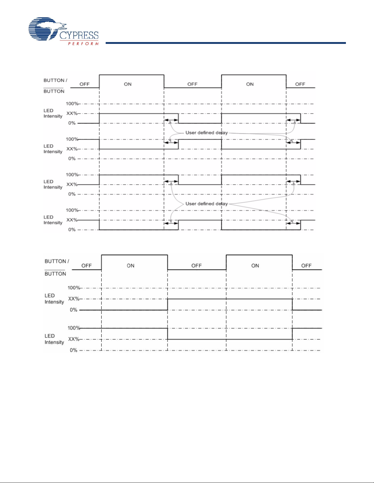
LED Dimming
To change the brightness and intensity of the LEDs, the host
master (MCU, MPU, DSP, and so on) must send I
and program the PWM registers to enable output pins, set duty
cycle, and mode configuration. The single PWM source is
connected to all GPIO pins and has a common user defined duty
cycle. Each PWM enabled pin has two possible outputs: PWM
and 0/1 (depending on the configuration). Four different modes
of LED dimming are possible, as shown in “LED Dimming Mode
1: Change Intensity on ON/OFF Button Status” on page 11 to
“LED Dimming Mode 4: Toggle Intensity on ON/OFF or OFF/ON
Button Transitions” on page 12. The operation mode and duty
cycle of the PWM enabled pins is common. This means that one
pin cannot behave as in Mode1 and another pin as in Mode 2.
2
C commands
Document Number: 001-54606 Rev. *A Page 10 of 31
[+] Feedback
Page 11

CY8C20110/CY8C20180/CY8C20160
CY8C20140/CY8C20142
LED Dimming Mode 1: Change Intensity on ON/OFF Button Status
LED Dimming Mode 2: Flash Intensity on ON Button Status
Document Number: 001-54606 Rev. *A Page 11 of 31
[+] Feedback
Page 12
CY8C20110/CY8C20180/CY8C20160
CY8C20140/CY8C20142
LED Dimming Mode 3: Hold Intensity After ON/OFF Button Transition
LED Dimming Mode 4: Toggle Intensity on ON/OFF or OFF/ON Button Transitions
Note LED DIMMING is available only in CY8C20110.
Document Number: 001-54606 Rev. *A Page 12 of 31
[+] Feedback
Page 13
CY8C20110/CY8C20180/CY8C20160
CY8C20140/CY8C20142
Register Map
Name
Register
Address
(in Hex)
Access
Writable Only in
SETUP Mode
INPUT_PORT0 00 R 00 0.1
INPUT_PORT1 01 R 00 0.1
STATUS_POR0 02 R 00 0.1
STATUS_POR1 03 R 00 0.1
OUTPUT_PORT0 04 W 00 0.1
OUTPUT_PORT1 05 W 00 0.1
CS_ENABL0 06 RW YES 00 11
CS_ENABLE 07 RW YES 00 11
GPIO_ENABLE0 08 RW YES 00 11
GPIO_ENABLE1 09 RW YES 00 11
INVERSION_MASK0 0A RW 00 0.11
INVERSION_MASK1 0B RW 00 0.11
INT_MASK0 0C RW YES 00 11
INT_MASK1 0D RW YES 00 11
STATUS_HOLD_MSK0 0E RW 03/1F
STATUS_HOLD_MSK1 0F RW 03/1F
DM_PULL_UP0 10 RW YES 00 11
DM_STRONG0 11 RW YES 00 11
DM_HIGHZ0 12 RW YES 00 11
DM_OD_LOW0 13 RW YES 00 11
DM_PULL_UP1 14 RW YES 00 11
DM_STRONG1 15 RW YES 00 11
DM_HIGHZ1 16 RW YES 00 11
DM_OD_LOW1 17 RW YES 00 11
PWM_ENABLE0
PWM_ENABLE1
PWM_MODE_DC
PWM_DELAY
[8]
[8]
[8]
[8]
18 RW 00 0.1
19 RW 00 0.1
1A RW 00 0.1
1B RW 00 0.1
OP_SEL_00 1C RW 00 0.12 11
OPR1_PRT0_00 1D RW 00 0.12 11
OPR1_PRT1_00 1E RW 00 0.12 11
OPR2_PRT0_00 1F RW 00 0.12 11
OPR2_PRT1_00 20 RW 00 0.12 11
OP_SEL_01 21 RW 00 0.12 11
OPR1_PRT0_01 22 RW 00 0.12 11
OPR1_PRT1_01 23 RW 00 0.12 11
OPR2_PRT0_01 24 RW 00 0.12 11
OPR2_PRT1_01 25 RW 00 0.12 11
OP_SEL_02 26 RW 00 0.12 11
OPR1_PRT0_02 27 RW 00 0.12 11
OPR1_PRT1_02 28 RW 00 0.12 11
Factory Default Values
[4]
of Registers
(in Hex)
I2C Max ACK Time in
Normal Mode (ms)
[5]
[5]
0.11
0.11
I2C Max ACK Time
in Setup Mode (ms)
Document Number: 001-54606 Rev. *A Page 13 of 31
[+] Feedback
Page 14

CY8C20110/CY8C20180/CY8C20160
CY8C20140/CY8C20142
Register Map
Name
(continued)
Register
Address
(in Hex)
Access
Writable Only in
SETUP Mode
[4]
Factory Default Values
of Registers
(in Hex)
I2C Max ACK Time in
Normal Mode (ms)
I2C Max ACK Time
in Setup Mode (ms)
OPR2_PRT0_02 29 RW 00 0.12 11
OPR2_PRT1_02 2A RW 00 0.12 11
OP_SEL_03 2B RW 00 0.12 11
OPR1_PRT0_03 2C RW 00 0.12 11
OPR1_PRT1_03 2D RW 00 0.12 11
OPR2_PRT0_03 2E RW 00 0.12 11
OPR2_PRT1_03 2F RW 00 0.12 11
OP_SEL_04 30 RW 00 0.12 11
OPR1_PRT0_04 31 RW 00 0.12 11
OPR1_PRT1_04 32 RW 00 0.12 11
OPR2_PRT0_04 33 RW 00 0.12 11
OPR2_PRT1_04 34 RW 00 0.12 11
OP_SEL_10 35 RW 00 0.12 11
OPR1_PRT0_10 36 RW 00 0.12 11
OPR1_PRT1_10 37 RW 00 0.12 11
OPR2_PRT0_10 38 RW 00 0.12 11
OPR2_PRT1_10 39 RW 00 0.12 11
OP_SEL_11 3A RW 00 0.12 11
OPR1_PRT0_11 3B RW 00 0.12 11
OPR1_PRT1_11 3C RW 00 0.12 11
OPR2_PRT0_11 3D RW 00 0.12 11
OPR2_PRT1_11 3E RW 00 0.12 11
OP_SEL_12 3F RW 00 0.12 11
OPR1_PRT0_12 40 RW 00 0.12 11
OPR1_PRT1_12 41 RW 00 0.12 11
OPR2_PRT0_12 42 RW 00 0.12 11
OPR2_PRT1_12 43 RW 00 0.12 11
OP_SEL_13 44 RW 00 0.12 11
OPR1_PRT0_13 45 RW 00 0.12 11
OPR1_PRT1_13 46 RW 00 0.12 11
OPR2_PRT0_13 47 RW 00 0.12 11
OPR2_PRT1_13 48 RW 00 0.12 11
OP_SEL_14 49 RW 00 0.12 11
OPR1_PRT0_14 4A RW 00 0.12 11
OPR1_PRT1_14 4B RW 00 0.12 11
OPR2_PRT0_14 4C RW 00 0.12 11
OPR2_PRT1_14 4D RW 00 0.12 11
CS_NOISE_TH 4E RW 28 0.11 11
CS_BL_UPD_TH 4F RW 64 0.11 11
CS_SETL_TIME 50 RW YES A0 35
CS_OTH_SET 51 RW YES 00 35
CS_HYSTERISIS 52 RW 0A 0.11 11
Document Number: 001-54606 Rev. *A Page 14 of 31
[+] Feedback
Page 15

CY8C20110/CY8C20180/CY8C20160
CY8C20140/CY8C20142
Register Map
Name
(continued)
Register
Address
(in Hex)
Access
Writable Only in
SETUP Mode
[4]
Factory Default Values
of Registers
(in Hex)
I2C Max ACK Time in
Normal Mode (ms)
I2C Max ACK Time
in Setup Mode (ms)
CS_DEBOUNCE 53 RW 03 0.11 11
CS_NEG_NOISE_TH 54 RW 14 0.11 11
CS_LOW_BL_RST 55 RW 14 0.11 11
CS_FILTERING 56 RW 20 0.11 11
CS_SCAN_POS_00 57 RW YES FF 11
CS_SCAN_POS_01 58 RW YES FF 11
CS_SCAN_POS_02 59 RW YES FF 11
CS_SCAN_POS_03 5A RW YES FF 11
CS_SCAN_POS_04 5B RW YES FF 11
CS_SCAN_POS_10 5C RW YES FF 11
CS_SCAN_POS_11 5D RW YES FF 11
CS_SCAN_POS_12 5E RW YES FF 11
CS_SCAN_POS_13 5F RW YES FF 11
CS_SCAN_POS_14 60 RW YES FF 11
CS_FINGER_TH_00 61 RW 64 0.14 11
CS_FINGER_TH_01 62 RW 64 0.14 11
CS_FINGER_TH_02 63 RW 64 0.14 11
CS_FINGER_TH_03 64 RW 64 0.14 11
CS_FINGER_TH_04 65 RW 64 0.14 11
CS_FINGER_TH_10 66 RW 64 0.14 11
CS_FINGER_TH_11 67 RW 64 0.14 11
CS_FINGER_TH_12 68 RW 64 0.14 11
CS_FINGER_TH_13 69 RW 64 0.14 11
CS_FINGER_TH_14 6A RW 64 0.14 11
CS_IDAC_00 6B RW 0A 0.14 11
CS_IDAC_01 6C RW 0A 0.14 11
CS_IDAC_02 6D RW 0A 0.14 11
CS_IDAC_03 6E RW 0A 0.14 11
CS_IDAC_04 6F RW 0A 0.14 11
CS_IDAC_10 70 RW 0A 0.14 11
CS_IDAC_11 71 RW 0A 0.14 11
CS_IDAC_12 72 RW 0A 0.14 11
CS_IDAC_13 73 RW 0A 0.14 11
CS_IDAC_14 74 RW 0A 0.14 11
[6]
75
76
77
78
[6]
[6]
[6]
I2C_ADDR_LOCK 79 RW 01 0.11 11
DEVICE_ID 7A R 42/40/60/80/10
[7]
0.11 11
DEVICE_STATUS 7B R 03 0.11 11
I2C_ADDR_DM 7C RW 00 0.11 11
Document Number: 001-54606 Rev. *A Page 15 of 31
[+] Feedback
Page 16

CY8C20110/CY8C20180/CY8C20160
CY8C20140/CY8C20142
Register Map
Notes
4. These registers are writable only after entering into setup mode. All the other registers available for read and write in Normal as well as in Setup mode.
5. The factory defaults of Reg 0x0E and 0x0F is 0x03 for 20142 device and 0x1F for 20140/60/80/10 devices.
6. The register 0x75- 0x78, 0x7D and 0x8A-0x8D are reserved.
7. The Device ID for different devices are tabulat ed in Table 5.
8. These registers are available only in CY8C20110.
Name
7D
(continued)
Register
Address
(in Hex)
[6]
Access
Writable Only in
SETUP Mode
Factory Default Values
[4]
of Registers
(in Hex)
I2C Max ACK Time in
Normal Mode (ms)
I2C Max ACK Time
in Setup Mode (ms)
SLEEP_PIN 7E RW YES 00 0.1 11
SLEEP_CTRL 7F RW 00 0.1 11
SLEEP_SA_CNTR 80 RW 00 0.1 11
CS_READ_BUTTON 81 RW 00 0.12 11
CS_READ_BLM 82 R 00 0.12 11
CS_READ_BLL 83 R 00 0.12 11
CS_READ_DIFFM 84 R 00 0.12 11
CS_READ_DIFFL 85 R 00 0.12 11
CS_READ_RAWM 86 R 00 0.12 11
CS_READ_RAWL 87 R 00 0.12 11
CS_READ_STATUSM 88 R 00 0.12 11
CS_READ_STATUSL 89 R 00 0.12 11
[6]
8A
[6]
8B
[6]
8C
[6]
8D
COMMAND_REG A0 W 00 0.1 11
Table 5. Device IDs
Part Number Device ID
CY8C 20142 42
CY8C 20140 40
CY8C 20160 60
CY8C 20180 80
CY8C 20110 10
Note All the Ack times specified are maximum values with all buttons enabled and filer enabl ed with maximum or der.
Document Number: 001-54606 Rev. *A Page 16 of 31
[+] Feedback
Page 17

CY8C20110/CY8C20180/CY8C20160
CY8C20140/CY8C20142
CapSense Express Commands
Note
9. The ‘W’ indicates the write transfer. The next byte of data represents the 7 bit I2C address.
Command
W 00 A0 00 Get firmware revision Setup/Normal 0
W 00 A0 01 Store current configuration to NVM Setup/Normal 120
W 00 A0 02 Restore factory configuration Setup/Normal 120
W 00 A0 03 Write NVM POR defaults Setup/Normal 120
W 00 A0 04 Read NVM POR defaults Setup/Normal 5
W 00 A0 05 Read current configurations (RAM) Setup/Normal 5
W 00 A0 06 Reconfigure device (POR) Setup 5
W 00 A0 07 Set Normal mode of operation Setup/Normal 0
W 00 A0 08 Set Setup mode of operation Setup/Normal 0
W 00 A0 09 Start scan Setup/Normal 10
W 00 A0 0A Stop scan Setup/Normal 5
W 00 A0 0B Get CapSense scan status Setup/Normal 0
[9]
Description
Executable
Mode
Duration the Device is not
accessible after ACK (in ms)
Register Conventions
This table lists the register conventions that are specific to this section.
Convention Description
RW Register has both read and write access
R Register has only read access
Document Number: 001-54606 Rev. *A Page 17 of 31
[+] Feedback
Page 18
CY8C20110/CY8C20180/CY8C20160
CY8C20140/CY8C20142
Layout Guidelines and Best Practices
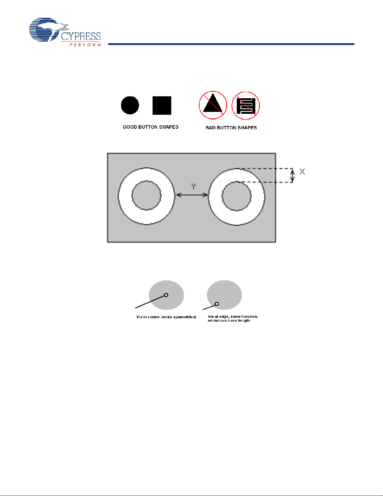
CapSense Button Shapes
Button Layout Design
X: Button to ground clearance (Refer to Table 6 on page 19)
Y: Button to button clearance (Refer to Table 6 on page 19)
Recommended via Hole Placement
Document Number: 001-54606 Rev. *A Page 18 of 31
[+] Feedback
Page 19

CY8C20110/CY8C20180/CY8C20160
CY8C20140/CY8C20142
Table 6. Recommended Layout Guidelines and Best Practices
Sl Category Min Max Recommendations/Remarks
1 Button Shape Solid round pattern, round with LED hole, rectangle with
2 Button Size 5 mm 15 mm 10 mm
3 Button-Button Spacing = Button
4 Button Ground Clearance 0.5 mm 2 mm Button ground clearance = Overlay Thickness [Y]
5 Ground Flood - Top Layer Hatched ground 7 mil trace and 45 mil grid (15% filling)
6 Ground Flood - Bottom Layer Hatched ground 7 mil trace and 70 mil grid (10% filling)
7 Trace Length from Sensor to
PSoC - Buttons
8 Trace Width 0.17 mm 0.20 mm 0.17 mm (7 mil)
9 Trace Routing Traces should be routed on the non sensor side. If any non
10 Via Position for the Sensors Via should be placed near the edge of the button/slider to
1 1 Via Hole Size for Sensor
Traces
12 Number of Vias on Sensor
Trace
13 CapSense Series Resistor
Placement
14 Distance between any
CapSense Trace to Ground
Flood
15 Device Placement Mount the device on the layer opposite to sensor. The
16 Placement of Components in 2
Layer PCB
17 Placement of Components in 4
Layer PCB
18 Overlay Thickness - Buttons 0 mm 2 mm 1 mm
19 Overlay Material Should to be non conductive material. Glass, ABS Plastic,
20 Overlay Adhesives Adhesive should be non conductive and dielectrically homog-
21 LED Back Lighting Cut a hole in the sensor pad and use rear mountable LEDs.
22 Board Thickness Standard board thickness for CapSense FR4 based designs
Ground
Clearance
200 mm <100 mm.
121
10 mm Place CapSense series resistors close to PSoC for noise
10 mil 20 mil 20 mil
round corners
8 mm [X]
CapSense trace crosses CapSense trace, ensure that intersection is orthogonal.
reduce trace length thereby increasing sensitivity.
10 mil
suppression.CapSense resistors have highest priority place
them first.
CapSense trace length between the device and sensors
should be minimum
Top layer - sensor pads and bottom layer - PSoC, other
components, and traces.
Top layer - sensor pads, second layer - CapSense traces,
third layer - hatched ground, bottom layer - PSoC, ot he r
components, and non CapSense traces
Formica
enous. 467MP and 468MP adhesives made by 3M are
recommended.
Refer the PCB layout below.
is 1.6 mm.
Document Number: 001-54606 Rev. *A Page 19 of 31
[+] Feedback
Page 20

CY8C20110/CY8C20180/CY8C20160
CY8C20140/CY8C20142
Example PCB Layout Design with Two CapSense Buttons and Two LEDs
Figure 6. Top Layer
Figure 7. Bottom Layer
Document Number: 001-54606 Rev. *A Page 20 of 31
[+] Feedback
Page 21

CY8C20110/CY8C20180/CY8C20160
CY8C20140/CY8C20142
Operating Voltages
For details on I2C 1x ACK time, refer to “Register Map” on page 13 and “CapSense Express Commands” on page 17. I2C 4x ACK
time is approximately four times the values mentioned in these tables.
CapSense Constraints
Parameter Min Typ Max Units Notes
Parasitic Capacitance (C
CapSense Sensor
Overlay Thickness 0 1 2 mm All layout best practices followed, properly
Supply Voltage Variation (V
) of the
P
)± 5%
DD
30 pF
tuned, and noise free condition.
Document Number: 001-54606 Rev. *A Page 21 of 31
[+] Feedback
Page 22

CY8C20110/CY8C20180/CY8C20160
CY8C20140/CY8C20142
Electrical Specifications
Absolute Maximum Ratings
Parameter Description Min Typ Max Unit Notes
T
STG
T
A
F32k u ILO frequency 15 32 64 kHz Calculations during sleep operations are
Tpowerup Power up time – 150 – ms VDD >= 3.1V
Tpowerup Power up time – 600 – ms 2.4V < VDD < 2.9V
V
DD
V
IO
V
IOZ
I
MIO
ESD Electro static discharge voltage 2000 – – V Human body model ESD
LU Latch up current – – 200 mA
Operating Temperature
Storage temperature –55 25 +100 °C Higher storage temperatures reduce data
retention time. Recommended storage
temperature is +25°C ± 25°C (0°C to 50°C).
Extended duration storage temperatures
above 65°C degrade reliability
Ambient temperature with power
–40 – +85 °C
applied
done based on ILO frequency.
Supply voltage on VDD relative to V
–0.5 – +6.0 V
SS
DC input voltage VSS – 0.5 – VDD + 0.5 V
DC voltage applied to tristate VSS – 0.5 – VDD + 0.5 V
Maximum current into any GPIO pin –25 – +50 mA
Parameter Description Min Typ Max Unit Notes
T
A
T
J
Ambient temperature –40 – +85 °C
Junction temperature –40 – +100 °C
DC Electrical Characteristics
DC Chip Level Specifications
Parameter Description Min Typ Max Unit Notes
V
DD
I
DD
ISB Deep Sleep mode current with POR
ISB Deep Sleep mode current with POR
ISB Deep Sleep mode current with POR
5V and 3.3V DC General Purpose I/O Specifications
This table lists guaranteed maximum and minimum specifications for the voltage and temperature ranges: 4.75V to 5.25V and
-40°C<
Parameter Description Min Typ Max Unit Notes
VOH1 High output voltage on Port 0 pins VDD – 0.2 – – V IOH < 10 µA, VDD > 3.10V, maximum of
VOH2 High output voltage on Port 0 pins VDD – 0.9 – – V IOH = 1 mA, VDD > 3.10V, maximum of
Supply voltage 2.40 – 5.25 V
Supply current – 1.5 2.5 mA Conditions are VDD = 3.10V, TA = 25°C
– 2.6 4 µA VDD = 2.55V, 0°C < TA < 40°C
and LVD active
– 2.8 5 µA VDD = 3.3V, –40°C < TA < 85°C
and LVD active
– 5.2 6.4 µA VDD = 5.25V, –40°C < TA < 85°C
and LVD active
TA<85°C, 3.10V to 3.6V -40°C<TA<85°C. Typical parameters apply to 5V and 3.3V at 25°C and are for design guidance only.
20 mA source current in all I/Os.
20 mA source current in all I/Os.
Document Number: 001-54606 Rev. *A Page 22 of 31
[+] Feedback
Page 23

CY8C20110/CY8C20180/CY8C20160
CY8C20140/CY8C20142
5V and 3.3V DC General Purpose I/O Specifications
Notes
10.The maximum sink current is 40 mA for 20140 and 20142 devices and for all other devices the maximum sink current is 60 mA
11.The maximum sink current per port is 20 mA for 20140 and 20142 devices and for all other devices the maximum sink current is 30 mA.
(continued)
This table lists guaranteed maximum and minimum specifications for the voltage and temperature ranges: 4.75V to 5.25V and
-40°C<TA<85°C, 3.10V to 3.6V -40°C<TA<85°C. Typical parameters apply to 5V and 3.3V at 25°C and are for design guidance only.
Parameter Description Min Typ Max Unit Notes
V
V
V
I
OH1
I
OH2
I
OL
OH3
OH4
OL
High output voltage on Port 1 pins VDD – 0.2 – – V IOH < 10 µA, VDD > 3.10V, maximum of
20 mA source current in all I/Os.
High output voltage on Port 1 pins VDD – 0.9 – – V IOH = 5 mA, VDD > 3.10V, maximum of
20 mA source current in all I/Os.
Low output voltage – – 0.75 V IOL = 20 mA/pin, VDD > 3.10, maximum of
40/60 mA sink current on even port pins and
of 40/60 mA sink current on odd port
[10]
pins.
High output current on Port 0 pins 0.01 – 1 mA VDD >= 3.1V, maximum of 20 mA source
current in all IOs
High output current on Port 1 pins 0.01 – 5 mA VDD >= 3.1V, maximum of 20 mA source
current in all IOs
Low output current – – 20 mA VDD >= 3.1V, maximum of 60 mA sink
current on pins P0_2, P1_2, P1_3, P1_4
and 60 mA sink current on pins P0_0, P0_1,
P0_3, P0_4, P1_0, P1_1
V
V
V
V
V
I
C
C
IL
IH
IL
IH
H
IL
IN
OUT
Input low voltage – – 0.75 V VDD = 3.10V to 3.6V.
Input high voltage 1.6 – – V VDD = 3.10V to 3.6V.
Input low voltage – – 0.8 V VDD = 4.75V to 5.25V.
Input high voltage 2.0 – – V VDD = 4.75V to 5.25V.
Input hysteresis voltage – 140 – mV
Input leakage – 1 – nA Gross tested to 1 µA.
Capacitive load on pins as input 0.5 1.7 5 pF Package and pin dependent.
Temp = 25°C.
Capacitive load on pins as output 0.5 1.7 5 pF Package and pin dependent.
Temp = 25°C.
2.7 DC General Purpose IO Specifications
Parameter Description Min Typ Max Unit Notes
V
OH1
V
OH2
V
OH3
V
OH4
V
OL1
Document Number: 001-54606 Rev. *A Page 23 of 31
High output voltage on Port 0 pins VDD – 0.2 – – V IOH <10 µA, maximum of 10 mA source
current in all IOs.
High output voltage on Port 0 pins VDD – 0.5 – – V IOH = 0.2 mA, maximum of 10 mA
source current in all IOs.
High output voltage on Port 1 pins VDD – 0.2 – – V IOH <10 µA, maximum of 10 mA source
current in all IOs.
High output voltage on Port 1 pins VDD – 0.5 – – V IOH = 2 mA, maximum of 10 mA
source current in all IOs.
Low output voltage – – 0.75 V IOL = 10 mA/pin, VDD > 3.10, maximum of
20/30 mA sink current on even port pins and
of 20/30mA sink current on odd port pins.
[11]
[+] Feedback
Page 24

CY8C20110/CY8C20180/CY8C20160
CY8C20140/CY8C20142
2.7 DC General Purpose IO Specifications
I
I
I
V
V
V
V
I
C
C
OH
OL1
OL2
IL
IH1
IH2
H
IL
IN
OUT
High output current 0.01 – 2 mA VDD <= 2.9V, maximum of 10 mA source
current in all IOs
Low output current on Port 0 pins – – 10 mA VDD <= 2.9V, maximum of 30 mA sink
current on pins P0_2, P1_2, P1_3, P1_4
and 30 mA sink current on pins P0_0, P0_1,
P0_3, P0_4, P1_0, P1_1
Low output current – – 20 mA VDD <= 2.9V, maximum of 50 mA sink
current on pins P0_2, P1_2, P1_3, P1_4
and 50 mA sink current on pins P0_0, P0_1,
P0_3, P0_4, P1_0, P1_1
Input low voltage – – 0.75 V VDD = 2.4 to 2.90V and 3.10V to 3.6V.
Input High voltage 1.4 – – V VDD = 2.4 to 2.7V.
Input High voltage 1.6 – – V VDD = 2.7 to 2.90V and 3.10V to 3.6V.
Input hysteresis voltage – 60 – mV
Input leakage – 1 – nA Gross tested to 1 µA.
Capacitive load on pins as input 0.5 1.7 5 pF Package and pin dependent.
Temp = 25°C.
Capacitive load on pins as output 0.5 1.7 5 pF Package and pin dependent.
Temp = 25°C
2.7V DC Spec for I2C Line with 1.8V External Pull Up
This table lists guaranteed maximum and minimum specifications for the voltage and temperature ranges: 2.4V to 2.9V and 3.10V to
3.60V, and -40°C<
drain and pulled up to 1.8V externally.
TA <85°C, respectively. Typical parameters apply to 2.7V at 25°C. The I2C lines drive mode must be set to open
Parameter Description Min Typ Max Unit Notes
V
V
V
C
R
OLP
IL
IH
I2C
PU
Low output voltage – – 0.4 V IOL=5 mA/pin
Input low voltage – – 0.75 V V
Input high voltage 1.4 – – V V
= 2.4 to 3.6V.
DD
= 2.4 to 3.6V.
DD
Capacitive load on I2C pins 0.5 1.7 5 pF Package and pin dependent.
Temp = 25°C.
Pull up resistor 4 5.6 8 kΩ
DC POR and LVD Specifications
Parameter Description Min Typ Max Unit Notes
V
must be greater than or equal to 2.5V
DD
during startup or internal reset.
V
V
V
V
V
V
PPOR0
V
PPOR1
VLVD0
VLVD2
VLVD6
VDD Value for PPOR Trip
V
= 2.7V
DD
V
= 3.3V, 5V
DD
VDD Value for L VD Trip
VDD= 2.7V
VDD= 3.3V
VDD= 5V
–
–
2.39
2.75
3.98
2.36
2.60
2.45
2.92
4.05
2.40
2.65
2.51
2.99
4.12
Document Number: 001-54606 Rev. *A Page 24 of 31
[+] Feedback
Page 25

CY8C20110/CY8C20180/CY8C20160
CY8C20140/CY8C20142
DC Flash Write Specifications
Note
12.Commands involving flash writes (0x01, 0x02, 0x03) and flash read (0x04) must be executed only within the same VCC voltage range detected at POR (power on, or
command 0x06) and above 2.7V.
This table lists guaranteed maximum and minimum specifications for the voltage and temperature ranges: 4.75V to 5.25V and
-40°C<TA<85°C, 3.10V to 3.6V and -40°C<TA<85°C or 2.4V to 2.90V and -40°C<TA<85°C, respectively. Ty pical parameters apply to
5V , 3.3V, or 2.7V at 25°C. These are for design guidance only. Flash Endurance and Retention specifications are valid only within the
range: 25°C±20°C during the flash write operation. It is at the user’s own risk to operate out of this temperature range. If flash writing
is done out of this temperature range, the endurance and data retention reduces.
Symbol Description Min Typ Max Units Notes
Vdd
I
DDP
Flash
Flash
IWRITE
Supply Voltage for Flash Write Operations 2.7 – – V
Supply Current for Flash Write Operations – 5 25 mA
Flash Endurance 50,000
ENPB
Flash Data Retention 10 – – Years
DR
[12]
– – – Erase/write cycles
CapSense Electrical Characteristics
Max (V) Typ (V) Min (V)
Conditions for Supply
Voltage
Result
3.6 3.3 3.1 <2.9 The device automatically reconfigures itself to work in
2.7V mode of operation.
>2.9 or <3.10 This range is not reco mmended for CapSense usage.
2.90 2.7 2.45 <2.4 5V The scanning for CapSense parameters shuts down
until the voltage returns to over 2.45V.
>3.10 The device automatically reconfigures itself to work in
3.3V mode of operation.
<2.4V The device goes into reset.
5.25 5.0 4.75 <4.73V The scanning for CapSense parameters shuts down
until the voltage returns to over 4.73V.
Document Number: 001-54606 Rev. *A Page 25 of 31
[+] Feedback
Page 26

CY8C20110/CY8C20180/CY8C20160
CY8C20140/CY8C20142
AC Electrical Specifications
5V and 3.3V AC General Purpose I/O Specifications
Parameter Description Min Max Unit Notes
TRise0 Rise time, strong mode,
Cload = 50 pF , Port 0
TRise1 Rise time, strong mode,
Cload = 50 pF , Port 1
TFall Fall time, strong mode,
Cload = 50 pF , all ports
2.7V AC General Purpose I/O Specifications
Parameter Description Min Max Unit Notes
TRise0 Rise time, strong mode,
Cload = 50 pF, Port 0
TRise1 Rise time, strong mode,
Cload = 50 pF, Port 1
TFall Fall time, strong mode,
Cload = 50 pF
AC I2C Specifications
15 80 ns V
15 50 ns V
= 3.10V to 3.6V and 4.75V to
DD
5.25V, 10% - 90%
= 3.10V to 3.6V, 10% - 90%
DD
10 50 ns VDD = 3.10V to 3.6V and 4.75V to
5.25V, 10% - 90%
15 100 ns VDD = 2.4V to 2.90V, 10% - 90%
15 70 ns VDD = 2.4V to 2.90V, 10% - 90%
10 70 ns VDD = 2.4V to 2.90V, 10% - 90%
Parame-
ter
I2C SCL clock frequency 0 100 0 400 kbps Fast mode not supported for
F
SCL
I2C Hold time (repeated ) START condition.
T
HDSTA
After this period, the first clock pulse is
Description
Standard
Mode
Min Max Min Max
4.0 – 0.6 – µs
Fast Mode
Units Notes
V
< 3.0V
DD
generated
I2C LOW period of th e SCL clock 4.7 – 1.3 – µs
T
LOW
I2C HIGH period of the SCL clock 4.0 – 0.6 – µs
T
HIGH
I2C Setup time for a repeated START condition 4.7 – 0.6 – µs
T
SUSTA
I2C Data hold time 0 – 0 – µs
T
HDDAT
I2C Data setup time 250 – 100 – ns
T
SUDAT
I2C Setup time for STOP condition 4.0 – 0.6 – µs
T
SUSTO
I2C BUS free time between a STOP and STAR T
T
BUF
condition
TSPI2C Pulse width of spikes suppressed by the
4.7 – 1.3 – µs
––050 ns
input filter
Document Number: 001-54606 Rev. *A Page 26 of 31
[+] Feedback
Page 27

CY8C20110/CY8C20180/CY8C20160
CY8C20140/CY8C20142
Figure 8. Definition of Timing for Fast/Standard Mode on the I
Note
13.The ‘W’ indicates the write transfer and the next byte of data represents the 7-bit I 2C address. The I2C addre ss is assu med to be ‘0 ’ in th e above examp les.
Similarly ‘R’ indicates the read transfer followed by 7-bit address and data byte read operations.
Appendix- Examples of Frequently Used I2C Commands
2
C Bus
Sl
No.
1 Enter into setup mode W 00 A0 08
2 Enter into normal mode W 00 A0 07
3 Load factory defaults to RAM
registers
4 Do a software reset W 00 A0 08
5 Save current configuration to flash W 00 A0 01
6 Load factory defaults to RAM
registers and save as user configuration
7 Enable GP00 as CapSense button W 00 A0 08
8 Read CapSense button(GP00)
scan results
9 Read CapSense button status
register
Requirement I2C commands
W 00 A0 02
W 00 A0 06
W 00 A0 08
W 00 A0 02
W 00 A0 01
W 00 A0 06
W 00 06 01
W 00 A0 01
W 00 A0 06
W 00 81 01
W 00 82
R 00 RD. RD. RD.
W 00 88
R 00 RD
[13]
Comment
Enter into setup mode
Do software reset
Enter into setup mode
Load factory defaults to SRAM
Save the configuration to flash. Wait for time specified
in “CapSense Express Commands” on page 17.
Do software reset
Enter into setup mode
Configuring CapSense buttons
Save the configuration to flash. Wait for time specified
in “CapSense Express Commands” on page 17.
Do software reset
Select CapSense button for reading scan result
Set the read point to 82h
Consecutive 6 reads get baseline, difference count and
raw count (all two byte each)
Set the read pointer to 88
Reading a byte gets status CapSense inputs
Document Number: 001-54606 Rev. *A Page 27 of 31
[+] Feedback
Page 28

CY8C20110/CY8C20180/CY8C20160
CY8C20140/CY8C20142
Ordering Information
Notes
14.Earlier termed as QFN package.
15.T
J
= TA + Power x θ
JA.
16.Higher temperatures may be required based on the solder melting point. Typical temperatures for solder are 220 ± 5°C with Sn-Pb or 245 ± 5°C with Sn- Ag-Cu paste.
Refer to the solder manufacturer specifications.
Ordering Code
Package
Diagram
Package Type
CY8C20110-LDX2I 001-09116 16 COL
[14]
Operating
T emperature
CapSense
Block
GPIOs XRES Pin
Industrial Yes 10 Yes
CY8C20110-SX2I 51-85068 16 SOIC Industrial Yes 10 Yes
CY8C20180-LDX2I 001-09116 16 COL
[14]
Industrial Yes 08 Yes
CY8C20180-SX2I 51-85068 16 SOIC Industrial Yes 08 Yes
CY8C20160-LDX2I 001-09116 16 COL
[14]
Industrial Yes 06 Yes
CY8C20160-SX2I 51-85068 16 SOIC Industrial Yes 06 Yes
CY8C20140-LDX2I 001-09116 16 COL
[14]
Industrial Yes 04 Yes
CY8C20140-SX2I 51-85068 16 SOIC Industrial Yes 04 Yes
CY8C20142-SX1I 51-85066 8 SOIC Industrial Yes 04 No
Note For die sales information, contact a local Cypress sales office or Field Applications Engineer (FAE).
Ordering Code Definition
Table 7. Thermal Impedances by Package
Package Typical θ
JA
[15]
16 COL[1] 46 °C/W
16 SOIC 79.96 °C/W
8 SOIC 127.22 °C/W
Table 8. Solder Reflow Peak Temperature
Package Minimum Peak Temperature
[16]
Maximum Peak Temperature
16 COL[1] 240 °C 260 °C
16 SOIC 240 °C 260 °C
8 SOIC 240 °C 260 °C
Document Number: 001-54606 Rev. *A Page 28 of 31
[+] Feedback
Page 29

CY8C20110/CY8C20180/CY8C20160
CY8C20140/CY8C20142
Package Diagrams
001-09116 *E
51-85068 *C
Figure 9. 16-Pin Chip On Lead 3 X 3 mm (Sawn) (001-09116)
Figure 10. 16-Pin (150-Mil) SOIC (51-85068)
Document Number: 001-54606 Rev. *A Page 29 of 31
[+] Feedback
Page 30

CY8C20110/CY8C20180/CY8C20160
CY8C20140/CY8C20142
Figure 11. 8-Pin (150-Mil) SOIC (51-85066)
Document Number: 001-54606 Rev. *A Page 30 of 31
[+] Feedback
Page 31
CY8C20110/CY8C20180/CY8C20160
CY8C20140/CY8C20142
Document History Page
Document Title: CY8C20110/CY8C20180/CY8C20160/CY8C20140/CY8C20142 CapSense® Express™ - Button Capacitive
Controllers
Document Number: 001-54606
Rev. ECN No.
Orig. of
Change
Submission
Date
Description of Change
** 2741726 SLAN/FSU 07/21/2009 New Data sheet
*A 2821828 SSHH/FSU 12/4/2009 - Add Contents
- Added new electrical specs including F32k u, Tpowerup, and several
output current specs.
- Noted that the flash reads must also be done at POR voltage (previously
only specified flash writes).
Sales, Solutions, and Legal Information
Worldwide Sales and Design Support
Cypress maintains a worldwide network of offices, solution centers, manufacturer’s representatives, and distributors. T o find the office
closest to you, visit us at Cypress Locations.
Products
Automotive
Clocks & Buffers
PSoC Solutions
psoc.cypress.com/solutions
PSoC 1 | PSoC 3 | PSoC 5
Interface
Lighting & Power Control
Memory
Optical & Image Sensing
PSoC
Touch Sensing
USB Controllers
Wireless/RF
© Cypress Semiconductor Corporation, 2009. The information contained herein is subject to change without notice. Cypress Semiconductor Corporation assumes no responsibility for the use of any
circuitry other than circuitry embodied in a Cypress product. Nor does it convey or imply any license under patent or other rights. Cypress products are not warranted nor intended to be used for medical,
life support, life saving, critical control or safety applications, unless pursuant to an express written agreement with Cypress. Furthermore, Cypress does not authorize its products for use as critical
components in life-support systems where a malfunction or failure may reasonably be expected to result in significant injury to the user. The inclusion of Cypress products in life-support systems
application implies that the manufacturer assumes all risk of such use and in doing so indemnifies Cypress against all charges.
Any Source Code (software and/or firmware) is owned by Cypress Semiconductor Corporation (Cypress) and is protected by and subject to worldwide patent protection (United States and foreign),
United States copyrigh t laws and interna tional tr eaty pr ovision s. Cypr ess here by gra nt s to lic ensee a p erson al, no n-excl usive , non- tran sferabl e license to copy, use, modify, create derivative works of,
and compile the Cypress Source Code and derivative works for the sole purpose of creating custom software and or firmware in support of licensee product to be used only in conju nction with a Cypress
integrated circuit as specified in the ap plicable agr eement. Any reprod uction, modificati on, translation, co mpilation, or re presentatio n of this Source Code except as spe cified above is prohibited wi thout
the express written permission of Cypress.
Disclaimer: CYPRESS MAKES NO WARRANTY OF ANY KIND, EXPRESS OR IMPLIED, WITH REGARD TO THIS MATERIAL, INCLUDING, BUT NOT LIMITED TO, THE IMPLIED WARRANTIES
OF MERCHANTABILITY AND FITNESS FOR A PARTICULAR PURPOSE. Cypress reserves the right to make changes without further notice to the materials described herein. Cypress does not
assume any liability arising out of the app licati on or us e of an y product or circ uit de scrib ed herei n. Cypr ess does n ot auth orize it s product s for use a s critical component s in life-suppo rt systems where
a malfunction or failure may reasonably be expected to result in significant injury to the user. The inclusion of Cypress’ product in a life-support systems application implies that the manufacturer
assumes all risk of such use and in doing so indemnifies Cypress against all charges.
Use may be limited by and subject to the applicable Cypress software license agreement.
Document Number: 001-54606 Rev. *A Revised December 16, 20 09 Page 31 of 31
CapSense Express™ and PSoC De s ign er™ ar e tr ad ema rks a n d PS oC® and Ca pS ens e® ar e r eg ist ered t rad em ark s of C ypre ss Sem i con duc tor Corp. All other tr adem arks or reg iste red tra demark s
referenced herein are property of the respective corporations. Purchase of I2C components from Cypress or one of its sublicensed Associated Companies conveys a license under the Philips I2C
Patent Rights to use these components in an I2C system, provided that the system conforms to the I2C Standard Specification as defined by Philips. All products and company names mentioned in
this document may be the trademarks of their respective holders.
[+] Feedback
 Loading...