

Low Cost VMEbus Interface
Controller Family
CY7C960
CY7C961
Cypress Semiconductor Corporation • 3901 North First Street • San Jose • CA 95134 • 408-943-2600
December 1994 – Revised March 1996
1CY7C96 1
Features
• 80-Mbyte-per-second block transfer rates
• All VME64 transactions provided, including A64/D64,
A40/MD32 transfers
• Auto Slot ID
• CR/CSR space
• All standard (Rev C) VMEbus transactions implemented
• VMEbus Interrupter
• No local CPU required
• Programmable from VMEbus, serial PROM, or local bus
• DRAM controller, including refresh
• On-chip DMA controller
• Local I/O controller
• Flexible VMEbus address scheme
• User-configured VMEbus response
• 64-pin TQFP, 10x10mm (CY7C960)
• 100-pin TQFP, 14x14mm (CY7C961)
Functional Description
The CY7C960 Slave VMEbus Interface Controller provides
the board designer with an integrated, full-featured VME64 interface. This 64-pin device can be programmed to handle every transaction defined in the VME64 specification. The
CY7C961 is based upon the CY7C960: additional features include Remote Master capability whereby the CY7C961 can be
commanded to move data as a VMEbus master. The
CY7C961 is packaged in a 100-pin outline.
The CY7C960 contains all the circuitry needed to c ontrol large
DRAM arrays and local I/O circuitry without the intervention of
a local CPU. There are no re gisters to rea d or write, n o complex command blocks to be constructed in memory. The
CY7C960 simply fetches its own configuration parameters
during the power-on reset period. After reset the CY7C960
responds appropriately to VMEbus activity and controls local
circuitry transparently.
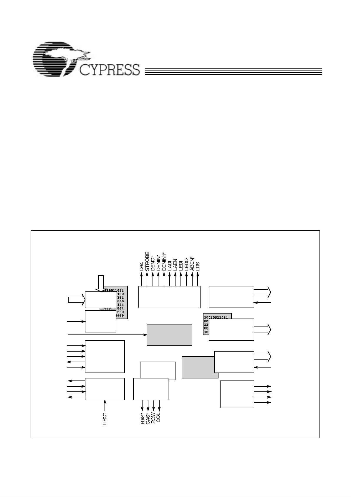
VMECONTROL
INTERF
ACE
CY7C960 Logic Block Diagram
c960–1
REGION/
AM TABLE
CY7C964CONTROLLER
POWER-ON
RESET
GENERATOR
AM [5:0]
SYSRESET*
AS*
DS0*
DS1*
DTACK*
WRITE*
CLK
REGION[3:0]
IRQ*
IACK*
IACKIN*
IACKOUT*
LOCAL ADDRESS
CONTROLLER
CHIP SELECT
OUTPUT PATTERN
TABLE
DATA BYTE
ENABLE
CONTROLLER
DATABYTE
LANE
DECODER
LOCAL
CONTROL
CIRCUIT
DRAM
CONTROLLER
REFRESH
CONTROLLER
TIMING
GENERATOR
VME INTERRUPT
INTERFACE
CS[5:0]
DBE[3:0]
LACK*
LDEN*
PREN*
SWDEN*
R/W
LA [7:1]
LWORD
CY7C960
CY7C961
2
REGION/
AMTABLE
CY7C964 CONTROLLER
POWER-ON
RESET
GENERATOR
AM[5:0]
SYSRESET*
AS*
DS0*
DS1*
DTACK*
WRITE*
BR*
BBSY*
BERR*
BGIN*
BGOUT*
CLK
REGION[3:0]
IRQ*
IACK*
IACKIN*
IACKOUT*
DATA BYTE
ENABLE
CONTROLLER
DATABYTE
LANE
DECODER
LOCAL
CONTROL
CIRCUIT
DRAM
CONTROLLER
REFRESH
CONTROLLER
TIMING
GENERATOR
VME
CONTROL
INTERFACE
VME
INTERRUPT
INTERFACE
CS[5:0]
DBE[3:0]
LACK*
LBERR*
LDEN*
PREN*
SWDEN*
R/W
LA[7:1]
LWORD
LOCAL
ADDRESS
CONTROLLER
CHIPSELECT
OUTPUT
PATTERN TABLE
LD[7:0]
DMA CHANNEL
REGISTERS
DMA
CONTROLLER
LOCK
CONTROLLER
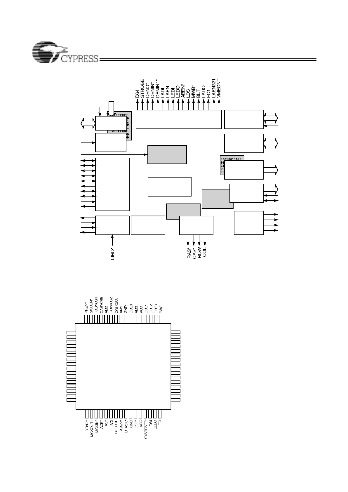
Top View
TQFP
c960–2
64 63 6162 60
2
3
1
32
33
34
12
13
15
14
16
4
5
3130
59 58
17
9
10
8
7
6
11
18 19 2120 22 23 2625 2728 2924
40
39
37
38
36
35
41
42
43
48
46
47
45
44
53 52 5051 4957 56
LA7
LA6
LA5
LA4
IRQ*
LA3
LA1
AM5
VCC
DS1*
LWORD
LAEN
LA2
LACK*
LIRQ*
LDEN*
CS0
CS1
AM3
GND
REGION1
REGION0
DENIN*
REGION2
5455
GND
LDS
DENIN1*
VCC
WRITE*
REGION3/CS2
AM4
CY7C960 Pin Configuration
CY7C961Logic Block Diagram
c960–3
CLK
SELECTLM
CY7C960
CY7C961
3
Functional Descriptio n (continued)
The CY7C960 controls a bridge between the VMEbus and local DRAM and I/O. Once programmed, the CY7C960 provides
activities such as DRAM refresh and local I/O handshaking in
a manner that requires no additional local circuitry. The VMEbus control signals are connected directly to the CY7C960.
The VMEbus address and data sign als are conn ected t o companion address/data transceivers which are controlled by the
CY7C960. The CY7C964 VMEbus Interface Logic Circuit is an
ideal companion device : the CY7C964 provides a slice of data
and address logic that has been optimized for VME64 transactions. In addition to providing the specified drive strength
and timing for VME64 transactions, the CY7C964 contains all
the circuitry needed to multiplex the address/data bus for multiplexed VMEbus transactions. It contains counters and latches neede d during BL T operations; and i t also contains address
comparators which can be used in the board’s Slave Address
Decoder. For a 6U or 9U application, four CY7C964 devices
are controlled by a single CY7C960. For 3U applications, the
CY7C960 controls two CY7C964 devices and an address
latch.
The design of the CY7C960 makes i t unnec essa ry to kno w the
details of the VMEbus transaction timing and protocol. The
complex VMEbus activities are translated by CY7C960 to simple local cycles involving a few familiar control signals. Similarly, it is not necessary to understand the operation of the
companion device, CY7C964: all control sequences for the
part are generated automatically by the CY7C96 0 in response
to VMEbus or local activity. If more information is desired, consult the CY7C964 chapter in the
VIC64 Design Notes
(avail-
able separately).
VMEbus transactions supported by the CY7C960 include D8,
D16, D32 (incl. UAT), MD32, D64, A16, A24, A32, A40, A64
single-cycle and block-transfer reads and writes, Read-Modify-Write cycles (incl. multiplexed), and Address-only (with or
without Handshake). The CY7C960 functions as a VMEbus
Interrupter, and supports the new Auto Slot ID standard and
CR/CSR space. The CY7C960 also handles LOCK cycles, although full LOCK support is not possible within the constraints
of the CY7C960 pinout. Full LOCK support is provided by the
CY7C961.
On the local side, no CPU is needed t o program the CY7C960 ,
nor to manage t ransac tions. All programmable parameters are
initialized through the use of either the VMEbus, a serial PROM, or
some other local circuit. As the CY7C960 incorporates a reliable
power-o n r eset c irc uit , pa r ame ter s are s el f- loa de d b y the dev ic e at
power-up or after a system reset. If the VMEbus is used to provide
paramet ers, a VMEbu s Mas ter p rovid es th e pro grammi ng in form ation using a protocol, described in the User’s Guide, which is compliant with the Aut o Slot ID pr otocol fro m the new VME6 4 speci fic ation.
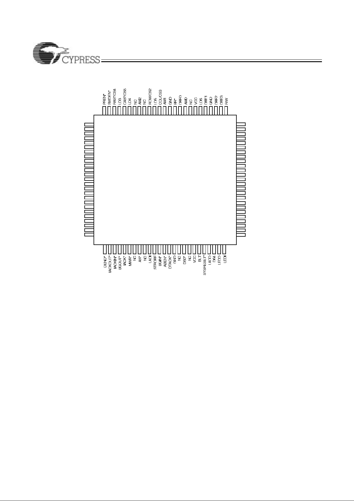
Top View
TQFP
10099 9798 96
2
3
1
4241
59
60
61
12
13
15
14
16
4
5
4039
95 94
17
26
9
10
8
7
6
11
27 28 3029 31 32 3534 3637 3833
67
66
64
65
63
62
68
69
70
75
73
74
72
71
89 88 8687 8593 92 84
LA7
LA6
LA5
LD7
LA4
SELECTLM*
LAEN321
IRQ*
LA3
GND
AM5
VCC
LA1
NC
LACK*
LIRQ*
LDEN*
LD1
CS0
VCC
AM3
AM4
BERR*
GND
VMECNT
REGION2
REGION3/CS2
9091
LBERR*
LA2
BBSY*
NC
VCC
LD2
CS1
NC
DS1*
NC
LWORD
FC1
LDS
DENIN1*
LAEN
LD0
CLK
NC
WRITE*
NC
REGION1
REGION0
DENIN*
18
19
20
21
22
23
24
25
83 82 81 80 79 78 77 76
58
57
56
55
54
53
52
51
43 44 4546 47 48 49 50
c960–4
CY7C961 Pin Configuration
 Loading...