


PRELIMINARY
Features
WAN and LAN ATM physi cal layer devic e
•
Provides complete physi cal layer t ransport of A TM cells
•
at:
—STS−3c/ STM−1 rate of 155.52 MHz
—STS−1 rate of 51.84 MHz
Compliant with ATM Forum User Netw or k Inter face 3. 1
•
specification
UTOPIA ATM inte rface
•
ATM cell processing including:
•
—HEC generation/verification
—Cell scrambli ng / d es c r ambling
—Rate adaption/idle cell filtering
—Local Flow Control
—Cell alignm ent
SONET frame processing including:
•
—Compliant with Bellcore GR−253, I.432,
T1.105, and G.709 for Jitter Tolerance and Jit ter
Generation
—Frame generation/recovery
—SO N ET scrambling/descrambling
—Frequency justification/pointer processing
Complete line interface including:
•
—C lock and data recovery
—Transmit timing derived from receiver or byte-rate
source
—SO NET com pliant PLL
—100K PECL compatible I/O
Alarm indications including:
•
—Loss Of Signal
—Out Of Frame, Loss Of Frame
CY7C955
AX™ ATM-SONET/SDH Transceiver
— Line Far E n d Recei ve Failure
—Line Alarm Indication Signal
— B1 Parity Error
—Loss Of Cell Alignment
—Loss O f Recei ve Data
Controller interface for internal int errupt and
•
configuration registers including:
—Error monitoring
—Status indication
—Device configuration
0.65µ Low Power CMOS
•
• 128-pin PQFP
Functional Description
The Cypress Semiconductor CY7C955 is a Transceiver chip
designed to carry ATM cells across SONET/SDH systems .
On the transmit side, ATM cells coming from the Utopia interface are bei ng mappe d into SONET/ SDH frames and then se rialized for transmission over fiber or twisted pair (through an
optical module or an equalizer chip).
On the receive side, serial SONET/SDH datastreams coming
from an optical module or an equalizer chip are being recovered by the intergrated clock and data recovery phase-locked
loop, framed, processed, and presented as parallel ATM cells
on the Receive Utopia Interface.
The CY7C955 can be use d in a Network Interface Card (NIC)
design to connect the segmentation and Reassembly (SAR)
chip to the optical modules or equalizer chi p.
The CY7C955 can also be used in work group or enterprise
switches to connect the I/O FIFOs of the switch fabric to the
optical module or equalizer in the interface boards.
The applications of the CY7C955 include adapters, switches,
routers, hubs , and proprietary systems.
T ABLE OF CONTENTS
Features 1
Functional Description 1
Pin Descriptions 2
Pin Configuratio n 7
Description 8
Transmit Section 8
Receive Section 10
Controller Interface (CI) 12
Loopback Oper ati on 16
SONET Overhead Description 17
CY7C955 Register Map 18
Electrical Characteristics 60
Capacitance 61
AC Test Loads and Waveforms 61
Switching Characteristics 61
Cypress Semiconductor Corporation
• 3901 North First Street • San Jose • CA 95134 • 408-943-2600
November 29, 1999
PRELIMINARY
CY7C955
T ABLE OF CONTENTS (continued)
Switching Wavef o rm s 63
Functional Timing Diagram 69
Interfa ce Termination and Biasing Schemes 73
Filter Pin Configurat ion 75
Ordering Info rmatio n 76
Package Diagram 77
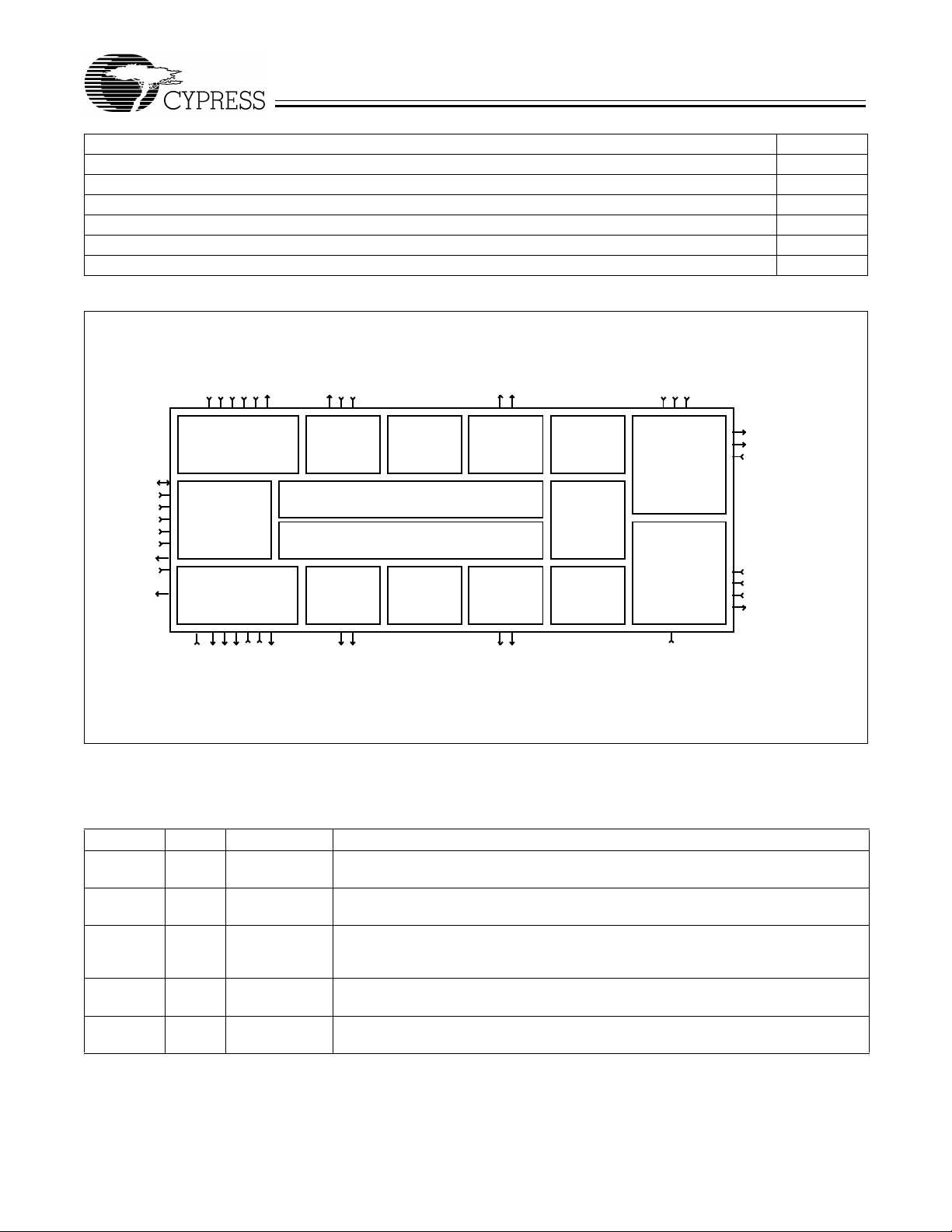
RATE1
TBYP
RATE0
Transmit
Clock
Transmit
Buffer
SONET/SDH
Clock
Recovery
RBYP
TXD±
TXC±
TRCLK±
ALOS±
RRCLK±
RXD±
RXDO±
7C955−1
D[7:0]
A[7:0]
ALE
RDB
WRB
CSB
INTB
RSTB
RALM
TDAT[7:0]
TSOC
TFCLK
TXPRTY
UTOPIA I/F
Transmit FIF O
4 Cell by 8 bit
Controller
Interface
UTOPIA I/F
Receive FIFO
4 Cell by 8 bit
TSEN
RSOC
RXPRTY
RDAT[7:0]
RFCLK
TWRENB
TCA
RRDENB
TCP
XOFF
TGFC
Transmit Transmit Transmit TransmitTransmit
ATM Cell
Processor
Configuration and Status
Register File
Error Monitoring
Receive Receive Receive ReceiveReceive
Processor
RCA
RCP
RGFC
TFPO
TCLK
Path
Overhead Overhead Overhead
PathATM Cell
Processor Processor Processor
Line Section
ProcessorProcessorProcessor
Rate
Selection
SectionLine
OverheadOverheadOverhead
RFP
RCLK
Multiplier &
Pin Descriptions
CY7C955 ATM-SONET/SDH Transceiver
Transmit Utopia Interface
Name Pin I/O Description
TDAT[7:0] 87−94 Input T ra nsmit Utopi a data: Byte-wid e data driv en from the ATM to PHY layer. TD AT[ 7] is the
MSB.
TPRTY 95 Input Transmit Utopia Data Parity: Data parity calculated over TDAT[7:0]. Odd parity is as-
sumed unless the TXPTYP bit (Reg–63, bit 7) is set to even parity
TSOC 96 Input Transmi t Utop ia St art of Cell: Assert TSOC HIGH when TDAT[7:0] contains the first
byte of an ATM cell. If TSOC is asserted sooner than 53 writ es after the pr eviou s SOC,
an error condition will be generated. This inpu t i s opti onal after the first TSOC pulse.
TFCLK 84 Input T ransmit Utopia Clock: Data transfer clock . Data is transferred to the AX on t he rising
edge of TFCLK when TWRENB is asserted (LOW).
TWRENB 85 Input T ransmit Ut opia Data Enable: Enab les the TFCLK input f or data transf er to the AX. This
signal is active LOW.
2

PRELIMINARY
Transmit Utopia Interface (continued)
Name Pin I/O Description
TCA 86 Output T ra nsmit Utopia Cell Av ailab le: An a ctive state on this si gnal in dicates t hat the T r ansmit
FIFO can acce pt at least N more cel ls ( 53 oc tets) of dat a where N and the act iv e st ate
of the signal (HIGH or LOW) are programmable through the config uration registers
(Reg−63H an d Reg−01H) . I n a s peci al case , i f Reg –63H bit2−3 is set to 00, Reg −01H,
bit 3 is set to 0, and TCALEVEL0 (Reg–63H, bit 1) set to 0. TCA will behave as an
active HIGH FULL indic ator.
Transmit ATM Interface
Name Pin I/O Description
XOFF 50 Input Transmi t Idle Cell: A HIGH state on this pin will force the ATM Cell Processor to send
TGFC 52 Input T r ansmi t Generic Flow Control : Thi s bit serial i nput pr ov ides t he abil ity to overwrite the
TCP 51 Ou tput Tr ansmit Sta rt Of GFC: This indicates th at the firs t bit of the GFC f or the ne x t cell read
Transmit Clock Generator
Name Pin I/O Description
TRCLK± 9−10 Differenti al In T ransmi t Input Cloc k: Accepts ei ther a diff erenti al PECL, or a TTL or a CMO S byte rate
TXC± 13−14 Differential Out Transmit Output Clock: Provides clock output for the transmit data. TXD± is updated
TXD± 15−16 Differential Out Transmit Data Output: Accepts NRZ encoded output data. This signal is updated on
TBYP 2 Input T ra nsmi t Cloc k Byp ass: When this input is held HI GH t he trans mit f requency mul tip lier
RATE0
RATE1
TCLK 54 Output Transmit Byte Reference: Byt e rate reference clock derived from the t ransmit line bit
TFPO 53 Output Tr ansmit Frame Reference. This signal is an 8-kHz frame rate reference that goes
97−98 Input RATE: When the RATE0 input i s HIGH the Transmit frequency generator and the Re-
an IDLE cell e ven i f there are cel ls to s end in th e Tr ans mit FIFO. XOFF is an async hronous input and has an integrated pull down resistor.
four bits of the ATM cell header GFC field. These bi ts may be optionally written during
the four TCLK cl ock periods following the assertion of the TCP output.
from the Transm it FIFO is expected on the TGFC pin during the next rising edge of
TCLK.
reference connected to TRCLK− with TRCLK+ grounded for the Transmit frequency
multiplier PLL. Optiona lly, this input can accept also the bit rat e reference when TBYP
is true (held HIGH). In th is mode the Transmit frequency multipl ier is b ypassed and the
bit rate clock is used directly for transmit side clocking.
on the falling edge of this signal. In the default setting, TXC is disabled if RATE0 is
HIGH and a 51.84-MHz cloc k if RA TE0 is LO W. XORTXC (Reg−04H, bit 6) ca n be used
to inve rt the default setting such tha t TXC is a 155.52- MHz clock i f RATE0 is HIG H and
is disabled w hen RATE0 is LOW.
the falling edge of TXC±.
is disabl ed and TRCLK± input is used dir ectly f or transmit s ide clocki ng. When t his input
is held LOW the transm it fre quenc y multi pli er mult ipli es the TRCLK± input b y 8, 24, or
8/3 (depending on the TREFSEL (Reg−06H, bit 0) setting to pr ovide the internal bit
rate clock .
ceive cl ock recov ery are selecte d to operate a t the STS−3c/STM−1 r ate of 155.52 MHz.
When the RATE0 pin is LO W, the Transmit frequency gener ator and the Rec eiv e c lock
recovery ar e s electe d to op er ate at the STS−1 rate of 51.8 4 MHz. RATE1 is for fact ory
testing use only and shoul d be ti ed HIGH. Both RATE0 and RATE1 have integrated
pull-up resistors.
rate.
HIGH during the transmission of the first A1 byte of the SONET/SDH frame . TFPO is
updated by the rising edge of TCLK.
CY7C955
Recei ve C l o ck R e covery
Name Pin I/O Description
RXD± 25−26 Differential In Receiv e Input Data: These line receiver inputs are connected to an internal Receive
PLL that recovers the embedded cloc k and data information. The incoming data rate
can be within one of two fre quency ranges depending on the state of the RATE0 pin.
3

PRELIMINARY
Recei ve C l o ck R e covery (continued)
Name Pin I/O Description
RXDO± 22−23 Differential Out Receive Output Data: These diff erential outputs represent the retimed v ersion of the
input data stream (RXD±) in normal mode and the buffe red v ersi on of the input datas tream (RXD±) in bypass mode. This output pair can be used as inputs to decision
feedback equalizers to correct for baseline wander. RXDO can be turned off to save
power by setting RXDOD (Reg−04H, bit 7) to 1.
RRCLK± 33−34 Differential In Receive Clock : These inpu ts are used t o clock in the diff ere ntial data ( RXD±) when the
Receive clock recov e ry block is by passed (RBYP=HI GH). If RBYP is LO W , RRCLK is
multiplied b y 8, 24, or 8/ 3 d epending on the set ting of RREFSEL ( Reg−07H, bit 0) and
use as a refer ence for the Receiv er PLL. Ref er to the s ection on “Interface T ermin ation
and Bias of Schemes” for connection examples to these pins.
RBYP 41 Input Receive Clock Bypass: When this input is HIGH the Receiver clock recovery block is
bypassed. In this mode the devi ce does not recover clock and data from the Receive
input data stream (RXD±) b ut i nstea d uses t he RRCLK± in puts t o cloc k t he d iff ere ntial
data into the devic e. When th is input is LOW the Receiver cl ock reco very bloc k reco vers
the clock and data fr om the input d ata stream. I n this mode a byte-rat e clock i s expecte d
on the RRCLK± inputs.
RCLK 57 Output Receive Byte Reference: Provides a byte-rate reference derived from the recov ered
bit- rate Receiv e clock. RALM, RCP, and RGFC are aligned with this clock.
RFP 58 Output Receive Frame Reference: This output provides a frame-rate reference clock aligned
to the SONET/SDH frame alignment bytes. RFP will pulse HIGH for one RCLK cycle
eve ry 125 seconds even at OOF and LOF situations.
LF+ 42 Input NC. This pin is for factory testing only.
LF–, LFO 43, 44 Input These are the PLL filter pins. Connect a 0.47-µF capacitor across LF– and LFO.
CY7C955
Receive ATM Interface
Name Pin I/O Description
RGFC 59 Output Receive Generic Flow Control: Thi s output provides the four bits of the current ATM
cell header GFC l ocati ons at ea ch suc cessive RCLK pulse. The RCP output indi cates
the first GFC bi t l ocat ion. This out put i s f orced LO W if the ATM Cell Processor has l ost
cell delineat ion.
RALM 63 Output Receive Interrupt: Thi s active HIGH signal is aligned with the RCLK b yte-rate cloc k and
signals the presence of LAIS, PAIS, LOS, LOF, LOP, or LCD.
RCP 60 Output Receive Start Of GFC: This output indicates the first bit of the G FC presented on the
RGFC output. This output goes HIGH for 1 RCLK cycle 6 byte times after the corre-
sponding cell is written into the Receive FIFO.
Receive Utopia Interface
Name Pin No I/O Description
RDAT[7:0] 70−71
74−79
RPRTY 82 Output Receive Utopia Data Parity: Data parity calculated ov er RDAT[7:0]. Odd parity is as-
RSOC 83 Output Rece ive Utopi a Start of Cell : Asserted HIGH when RD AT[7:0] contains the fi rst byte of
RFCLK 67 Input Receive Ut opia Cloc k: Data transf er cl ock. Data is transf erred from the AX on the rising
RRDENB 68 Input Receive Utopia Enable: Enab les the RFCLK input for dat a tr ansfers from the AX.
RCA 69 Output Receive Utopi a Cell Available: An active signal indicates that the Recei ve FIFO con-
Output Receiv e Utopia Data: Byte-wid e data driv en from th e PHY to ATM layer . RD AT[7] is the
MSB
sumed unless the TXPRTY bit is set to even parity by Reg−50H, bit 6.
an ATM cell.
edge of RFCLK when RRDENB is asserted (LOW).
tains at least 1 or 4 more bytes of data. RCA is controlled by RCAINV (Reg−01H, bit
2) and RCALEVEL0 (Reg−59H, bit 2).
4

PRELIMINARY
Receive Utopia Interface (continued)
Name Pin No I/O Description
TSEN 66 Input Receive Output Enab le: This output oper ates in conjuncti on with the RRDENB output.
When TSEN is HIGH and RRDENB i s HIGH the Receive UTOPIA data b us (RDAT[7:0],
RPRTY, and RSOC) is three-stated. When TSEN is HIGH and RRDENB is LOW the
data bus is driven with the requested data. When TSEN is LOW the data bus will not
three-state.
Controller Interface
Name Pin No I/O Description
D[7:0] 110−112
115−118
A[7:0] 119−126 Input Address[7:0]: Address bus used to select the internal register f or reading or writing.
ALE 127 Input Address Latch Enable: When this in put is LO W the addr ess is l atched f rom the A[7: 0]
RDB 105 Input Read: This activ e LOW signal is us ed to read the internal regi ster. The AX dri ves D[7:0]
WRB 104 Input Write: This active LOW signal is used to write the internal regi sters. Data is latche d
CSB 100 Input Select: This activ e LOW device select has to be enabled duri ng regi ster accesses.
INTB 108 Output Interrupt: This active LOW open drain output transitions LOW when an unmasked
ALOS± 27−28 D iffer e n tia l In Carrier Detect: This diff erential input co ntrols t he recov ery functio n of the Receiv e PLL
RSTB 101 Input Reset : Thi s active LOW signal provide s a device reset. This line can be pulled LOW
VCLK 99 Input Factory test pin. Must be LOW for normal operation. VCLK has an i ntegrated pul l-down
I/O Data[7:0]: Bidirectional data bus used to transfer data to and from the internal config-
uration, status, and error monitori ng registers.
inputs. When this input is HIGH, the input is transpar ent. ALE has an integr ated pullup resistor.
when RDB and CSB are both LOW.
into the specified address register on the rising edge of WRB when CSB is LOW.
interrupt source i s active. This output transiti ons HIGH when the appropriate register
has been read. This inter rupt sig nals the most crit ical error s tates of th e de vice inc luding Loss of P oint er , Line Al arm Indicat ion Signal (LAIS) , Line Far End Receive F ailur e
(LFERF), Loss of Fr ame (LOF), Out of Fram e (OOF), Loss of Signal (LOS), and many
others.
and can be driven by th e carri er detect output from opti cal modules or from external
transition detection circuitry. When this input is at a Logic Low, the input data stream
(RXD±) is recovered normally by the Recei v e Cloc k Recov ery PLL. When this input is
at a Logic Hi gh, t he Recei v e PLL n o l onger aligns t o RXD±, but in ste ad alig ns with the
RRCLK * 8 frequency and the LOS alarm register (RDOOLV) will be set. Besides
differential PECL, the ALOS− input can be set to accept single ended PECL input if
ALOS+ is tied to GND . ALOS− has to be decoupled.
to put the CY7C95 5 into the po wer -down mode . RSTB has an i nteg rated pull -up resistor.
resistor.
CY7C955
Transmit Power
Name Pin No I/O Description
TXVDD 12 Power The Transmit Pad Power supplies the TXD± outputs. TXVDD is physically isolated from
TAVD1 4 Power The power pin for the transmit clock synthesizer reference circuitry. TAVD1 should be
TAVD2 6 Power The power pin for the transmit clock synthesizer oscillator. TAVD2 should be connected
TAVD3 8 Power The power pin for the transmit PECL inputs. TAVD3 should be connect ed to anal og +5V.
TVDDO 18 Power Power for TXC± and RXDO±.
the other de vice po wer pins and should be wel l regulated +5 V DC and noise- free for good
performance when dri ving category 5 unshielded twist pair cabling.
connected to anal og +5V.
to analog +5V.
5

PRELIMINARY
CY7C955
Receive Power
Name Pin No I/O Description
RAVD1 30 Power The power pin for receiv e cloc k and data reco very block reference ci rcuitry . RA VD1 should
be connected to analog +5V.
RAVD2 36 Power The power pin f or receive clock and data recovery block active loop filter and oscillator.
RAVD2 should be connected to analog +5V.
RAVD3 24 Power The power pin for the RXD± and ALOS± PECL inputs. RAVD3 should be connected to
analog +5V.
RAVD4 32 Power The power pin for the RRCLK± PECL inputs. RAVD4 should be connected to an al og +5V.
Core Power
Name Pin No I/O Description
V
V
DDI
DDO
20, 61,
107
55, 73,
81, 114
Power The core power pins should be connected to a well decoupled +5V DC in common with
V
.
DDO
Power The pad ring power pins should be connected to a well decoupled +5V DC in common
with V
DDI
.
Ground
Name Pin No I/O Description
TAVS1 5 Ground The ground pin for the transmit clock synthes izer reference circuitry. TAVS1 should be
connected to anal og GND.
TAVS2 7 Ground The ground pin for t he transmit clock synthesizer oscillat or. TAVS2 should be connec ted
to analog GND.
TAVS3 11 Ground The ground pin for the transmit PECL input s. TAVS3 shou ld be connected t o analog GND .
TXV
SS
17 Ground The transmit pad ground is the return path for the TXC± and TXD± outputs. TXVSS is
physically isolated fro m the other device ground pins and should be noise-fr ee for good
performance when dri ving category 5 unshielded twisted pair cabling.
RAVS1 31 Ground The ground pin f or receive clock an d data recovery bl ock reference ci rcuitry. RAVS1 shoul d
be connected to analog GND.
RAVS2 37 Ground The ground pin fo r receive cloc k and data recovery bl ock active l oop filter and oscillator.
RAVS2 should be connected to analog GND.
RAVS3 29 Ground The ground pin f or the RRCLK± PECL inputs. RA VS3 shoul d be connected to analog GND .
RAVS4 35 Ground The ground pin for the RSD± and ALOS± PECL inputs. RAVS4 should be connected to
analog GND.
RVSSO 21 Ground This pin is grounded for TXC± and RXDO±.
V
SSI
19, 62,
Ground The core ground (V
) pins should be connected to GND in common with V
SSI
SSO
.
106,48
V
SSO
56, 72,
Ground The pad ring ground (V
) pins should be connected to GND in common with V
SSO
SSI
.
80, 113,
49
V
SS
1, 38,
39, 46,
Ground These pins must be connected to GND for correct operati on.
47, 64,
65, 102,
103,
128
ATP1,
ATP2,
40, 3, 46I/O These Analog Test Points (ATPx) are for factory testing use only. These pins have to be
tied to GND for correct chip operation.
ATP3
6

Pin Configuration
PRELIMINARY
128-pin PQFP
CY7C955
Top Vi ew
VSS
TBYP
ATP 2
TAVD1
TAVS1
TAVD2
TAVS2
TAVD3
TRCLK–
TRCLK+
TAVS3
TXV
TXC+
TXC–
TXD+
TXD–
TXV
TVDDO
VSSI
VDDI
RVSS
RXDO+
RXDO–
RAVD3
RXD–
RXD+
ALOS–
ALOS+
RAVS3
RAVD1
RAVS1
RAVD4
RRCLK–
RRCLK+
RAVS4
RAVD2
RAVS2
VSS
VSS
ALE
1284312744126451254612447123481224912150120511195211853117541165511556114
1
2
3
4
5
6
7
8
9
10
11
DD
SS
12
13
14
15
16
17
18
19
20
21
22
23
24
25
26
27
28
29
30
31
32
33
34
35
36
37
38
394142
40
A[4]
A[5]
A[6]
A[7]
A[0]
D[6]
D[7]
A[1]
A[2]
A[3]
VSSO
VDDO
D[4]
D[5]
113
CY7C955
AX
ATM
SONET / SD H
TRANSCEIVER
D[3]
112
D[2]
111
D[1]
110
57
D[0]
109
58
INTB
108
59
VDDI
VSSI
10795106
60
61
WRB
RDB
10594104
62
639664
VSS
103
102
101
100
99
98
97
93
92
91
90
89
88
87
86
85
84
83
82
81
80
79
78
77
76
75
74
73
72
71
70
69
68
67
66
65
VSS
RSTB
CSB
VSS
RATE[0]
RATE[1]
TSOC
TPRTY
TDAT[7]
TDAT[6]
TDAT[5]
TDAT[4]
TDAT[3]
TDAT[2]
TDAT[1]
TDAT[0]
TCA
TWRENB
TFCLK
RSOC
RPRTY
VDDO
VSSO
RDAT[7]
RDAT[6]
RDAT[5]
RDAT[4]
RDAT[3]
RDAT[2]
VDDO
VSSO
RDAT[1]
RDAT[0]
RCA
RRDENB
RFCLK
TSEN
VSS
VSS
ATP 1
LFO
LF
VSS
VSS
RBYP
ATP3
TCP
VSSI
XOFF
VSSO
TCLK
TFPO
TGFC
VDDO
VSSO
RCP
RFP
RCLK
RGFC
VDDI
VSS
VSSI
RALM
−
LF+
7C955−2
7

PRELIMINARY
CY7C955
Description
Transmit Section
T ransmit Utopia Interface (TUI)
The transmit interface provides a simple access from the external environment to the ATM Transceiver. The operation of
this interface is compliant with the Utopia interface specification. The interface provides a 9-bit by 4-cell FIFO to decouple
the system interface from the ATM physical layer timing. 9-bit
words are c loc ke d i nto t he de vi ce thr ough a clo c ked FI FO s ystem interface. These 9 bits include an 8-bit data word along
with a Start Of Cell (SOC) indication. The interface also provides full and almost full indications (TCA). Maximum cl ock
rate for this interface is 33 MHz.
T ransmit ATM Cell Pr ocessor (TACP)
The ATM cell processor provides HEC generation, idle/unassigned cell header modificat ion, pa yload scr ambli ng, and GFC
insertion.
HEC Generator
The Header Error Check (HEC) code is contained i n the last
byte of the ATM cell header and is capable of single error correction and multiple error detecti on. When optionally generated, the Transmit ATM Cell Processor calc ulates a CRC−8 ov er
the first four bytes of the ATM cell header using the pol ynomi al
8
x
+ x2+ x + 1. The coset x6 + x4 + x2 + 1 is added (modulo 2)
to the residue of thi s funct ion. The HEC is calc ulated in accordance with ANSI T1.624−1993 and CCITT Reco mmendation
I.432. This HEC sequ ence i s plac ed in th e 5th b yte of the ATM
cell header.
Idle/Unassigned Cell Header Modification
Idle (Unassigned) cells are sent by the ATM cell processor
whenev er a complete cell is not contained within the Transmit
FIFO. This transforms the non-continuous cell input stream
into a continuous stream of assigned and unassigned cells.
The ATM cell processor provides the ability to overwrite the
Generic Flow Control (GFC), the Payload Type Indication
(PTI), and the Cell Loss Priority (CLP) fields of Idle (Unassigned) cells with the values contained in the corresponding
configura tion registe rs. VPI and VCI are set to zero in I dle (Unassigned) cells.
Payload Scrambler
The 48 bytes of the ATM payload are scrambled using a parallel implem entation of the polynomial x
CCITT Recommendation I.432. The scrambler can be optionally deselec ted.
GFC Insertion
The transmit ted GFC field of an ATM cell can be derived fr om
different sources. For assigned cells, the default is from pins
TDAT[7:0]. For Idle (Unassigned) cells, the default is from
GFC[3:0] (Reg−61H, bit 7−bit 4). However, if any bit of
TGFCE[3:0] (Reg−67H, bit 7−bit4) is set, the corresponding
transmitted G FC location will instead be taken from the serial
TGFC (pin 52) input following the functional timing specifications described in the section on Transmit GFC Serial Link
Interface.
43
+ 1 as described in
Transmit SONET Path Overhead Processor (TPOP)
The SONET path ov erhe ad proces sor provi des pa y load poi nter alignment (H1, H2), path overhead insertion, and insertion
of the Synchron ous Payload Env elope (SPE). ATM cells (bot h
assigned and unassi gned ) are in serted into the SPE f or trans mission in the SONET frame
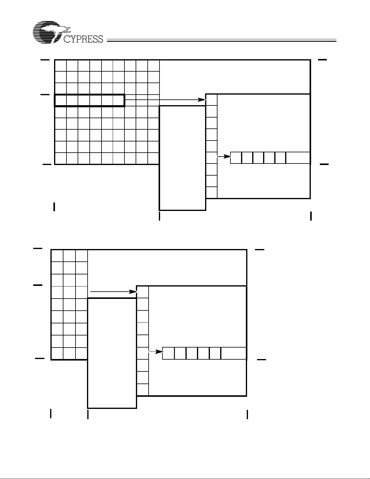
SONET Overhead Insertion
The SONET/SDH STS−3c/STM−1 frame st ructur e is sho wn in
Figure 1 and the SONET STS−1 frame structure is shown in
Figure 2. The SONET fram e occurs once every 125 µs and is
transmitted beginning with the A1 bytes, followed by the A2
bytes, C1 by tes, 261 by tes (87 bytes for S TS−1) of the Synchronous Payload Envelope (SPE), B1 bytes, etc., until the
entire frame is tr ansmitted.
The TPOP generates the H1 and H2 bytes that indicate the
beginning of the SPE and the H4 byte that indicates the ATM
cell offset within the SPE. The default initial value for H1 and
H2 pointer is 522, meaning that the first byte of the SPE (J1)
corresponding to a frame actually starts after the C1 byte of
the next frame.
In the def ault case des cribed abov e, a 6h i s present i n the New
Data Flag (NDF) portion of the first H1 (bits 0−4), a 2h is
present in bits 5−7 and a 0Ah is present in the first H2 byte.
The remaining H1 b ytes f or STS−3c/STM−1 are s et to 93h and
the remaining H2 b ytes ar e set t o FF h which i s the c onca tenation indication for the J1 pointer. The Pointer Action by te, H3,
is set to 00h. During Path AIS all of the H1 and H2 bits are set
to 1.
The STS path trace J1 is set to all zero s. The path BIP−8 (B3)
byte provides path error monitoring. This function calculates
the bit-inte rleav ed parity- 8 code usin g ev en parity o ve r the pre vious SPE before scrambling and is inserted into the current
B3 byte before scrambling. Bit-interleaved parity-8 forces the
number of 1s in the xth bit of every byte in the previous SPE
plus the xth bit of the B3 by te in t he curre nt SPE to be an even
number.
The path signal level indicator, C2, defaults to 13h.
The path status, G1, has several functions. Bits 1 through 4
are used to indicat e Far End Block Errors (FEBE) derived by
counting the nu mber of BIP−8 error s occurred in t he last fr ame
received. Valid codes are 0 through 8. If more than 8 errors
have a ccum ulated since the last, frame the maxim um value is
sent with the curr ent fr ame , the F EBE counter is decr emented
by 8, and the remaining errors are sent with the next frame.
FEBE may be inserted through register control for diagnostic
purposes. Bits 1 through 4 can also be used to transmit Far
End Receive Failures by setting these bits to 9 (1001). This
error indicat es to the far en d that cell deli neation has been lost .
Bit 5 can be used to generate a yellow alarm condition. The
default v alue for this bit is 0 (no alarm).
The multi-frame indicator, H4, is used to ind icate the first ATM
cell and may take on values of 00 to 34h.
The remaining bytes, F2, Z3, Z4, and Z5, are not used by the
SONET path processing and ar e set to 00h upon transmiss ion.
When operating in STS−1 mode, SPE columns 30 and 5 9 can
be configured as fixed stuff columns.
8
PRELIMINARY
.
A1
A1 A1 A2 A2 A2 C1 C1 C1
CY7C955
B1
E1 F1
Section
D1 D2 D3
H1
H1 H1 H2 H2 H2 H3 H3 H3
B2
B2 B2 K2
K1
D4 D5 D6
Line
D7 D8 D9
D10 D11 D12
Z1 Z1 Z1 Z2 Z2
9Bytes
Z2
E2
Figure 1. STS−3c/STM−1 Framing Form at
Payload
J1
B3
C2
G1
F2
H4
Z3
Z4
Z5
Path
Payload
HD1 HD2 HD3 HD4 HEC PAYLOAD
Bytes
261
7C955−3
Bytes
9
A1
B1
D1 D2 D3
H1
B2
D4 D5 D6
Line Section
D7 D8 D9
D10D11 D12
Z1 Z2
A2 C1
E1 F1
H2 H3
K1
E2
3Bytes
K2
Payload
J1
B3
C2
G1
F2
H4
Z3
Z4
Z5
Path
Payload
HD1 HD2 HD3 HD4 HEC PAYLOAD
87
Bytes
Bytes
9
7C955−4
Figure 2. STS−1 Framing Format
9

PRELIMINARY
CY7C955
T ransmit SONET Line Overhead Processor (TLOP)
The Transmit SONET line overhead processor (TLOP) provides B IP−8/24 generation and line level alarms.
The BIP−8/24 code is calculated as if the STS−3c frame was
composed of three STS−1s. The f irst B2 byte is calcu lated over
the firs t STS−1 frame, the second B2 byte over the second
STS−1 frame a nd the thir d B2 b yte ov er the t hird STS−1 frame.
Each B2 bit is calc ulated ov er t he line and SPE portions of th e
previou s frame befor e scramb ling using ev en parity and inserted into the current fram e befor e scrambl ing. For STS−1 RATE,
a BIP−8 is calculated over the entire SPE and line overhead
and placed in B2.
The Line Alarm Indicat ion Signal (LAIS), is as serted by changing all bits of the SONET f rame into 1 bef ore scramb ling . LAIS
generation is controlled by a register setting ( R eg−14H, bit 0).
The Line Far End Receive Failure (LFERF), also called Line
RDI, is indicated by pl acing a 110 pattern in bits 6,7, and 8 of
the first K2 byte. LFERF can be asserted under register
(Reg−20H, bit 0) control.
The Line Fa r End Block Err ors (LFEBE) are loca ted in the third
Z2 byte and indicate the number of B2 errors in the previous
frame interval . Legal v alues f or th is by te are 00 h throug h 18h.
All bytes of the line data com munication channel (D4−D12)
and all other unu sed bytes are encoded to 00h.
T ransmit SONET Section Overhead Processor (TSOP)
The Transmit SONET Line Overhead Processor (TSOP) provides A1,A2 framing pattern generation, section BIP−8 (B1)
insertion, secti on level alarm insertion, and fram e scrambling.
The A1 and A2 bytes pro vide a fr aming pattern fo r frame ali gnment. All A1 bytes are coded to F6h and all A2 bytes are coded
to 28h. These bytes are not scrambl ed upon transmission.
The STS−1 identification byt es, C1, are used for framing and
de-interleav ing purposes and are coded the order in their appearance in the STS−3c frame. The first C1 byte is coded to
01h, the second to 02h, and the t hird to 03h.
The section BIP−8 (B1) is the byte-interleaved par ity-8 calculated over all byt es of the previ ous fram e after scramb l ing and
inserted into the current frame before scrambling.
The bytes of the se ction dat a commun ication cha nnel , D1−D3
and the remaining unused bytes are set to 00h.
The frame is scr ambl ed prior to tr an smissi on with the gener a ting polynomial x
scrambled. The scrambler runs continuously through the
frame and reset s at the beginning of the next transmission
frame. The scrambler may be optionally disabled.
T ransmit Clock Generator (TCG)
The TCG accepts a byte-rate transmit clock from TRCLK that
operates at either 19.44 MHz for STS−3c/STM−1 RATE or at
6.48 MHz for STS−1 RATE. The Transmit PLL multiplies this
byte-rate reference by eight to produce the bit-rate clock used
by the parallel-to-serial converter. Optionally a bit-rate source
can be taken from an external source (TBYP = 1) or from the
Receive Clock Recovery block when in loop-time mode
(LOOPT = 1). In loop-time mode the recovered clock is used
to provide timing to the transmitte r.
7
+ x6 + 1. The A1, A2, and C1 bytes are not
Parallel to Serial Converter (PSC)
The PSC converts the parallel data from t he TSOP to serial
data. The bit rate cloc k is derived from the Transmit Cloc k Generator. The serialized data and aligned output clock are presented to the Transmit Output Mult iplexer.
Transmit Output Multiplexer (TOM)
The TOM selects between the serialized output data stream
and associated clock provided by the PSC and the recovered
data and clock from the Receive Clock Recovery block for
transmissi on based on the state of the local loop back enable
(LLE) register (Reg−05H, bit 2). When LLE = 1 the recovered
data and recovered clock is sel ected for ou tput on th e tra nsmi t
data lines (TXD±) and the transmit clock lines (TXC±). The
output signal is 100K compatible differential Positive-referenced ECL (PECL) signal capable of driving any copper or
fiber based media with impedances as LOW as 50Ω.
Receiv e Section
Receive Clock Recovery (RCR)
The RCR provides clock and data recovery from an incoming
differential PECL data stream. Clock and data are recovered
from the incoming differential PECL data stream without the
need for external buffering and AC-coupling. The built-in line
receiver inputs have a wide common-mode range (2.5−5V)
and the ability t o recei v e signal s wit h as littl e as 200 m V diff er ential volt age. They are compat ible with all PE CL signals. They
are compatib le with a ll PECL signal s driv en by optical modul es
or twisted-pair equalizers. The Receive PLL uses the RRCLK
as a byte-rate reference. This input is multiplied by 8 and is
used to impro ve PL L lock time and to provid e a center frequency for operat ion in the absence of input data stream transit ions.
The receiver can recover clock and data in two different frequency ranges depending on the state of the RATE0 pin. To
insure accurate data and clock recovery, the received data
stream must be within 1000 ppm of RRCLK * 8 (The PLL will
declare Out Of Lock if the data rate is different from REFCLK
x 8 by more than 2000 ppm. The PLL will remain Out Of Lock
until the data rate pulls back to within 700 ppm of REFCLK x
8 frequency). The standards, however, specify that the
RRCLK*8 frequency accurac y be within 20−100 ppm. The wid er frequency toler ance r a nge of the CY7C955 i s a n adv ant age
that allows for higher frequenc y tol eranc e in be nch tes ting setups.
A Loss of Signal (ROOLV = 1) is declare d when no transitions
have been detect ed on the incoming data st ream for more than
512 bit-times. LOS is cleared whe n two valid framing patterns
(A1, A2) have been found and the intervening data does not
contain a period that vio lat es the minimum transit ions limit.
Serial to Paral lel Conversion (SPC)
The SPC conv erts bit serial data to byt e s erial dat a fro m ei ther
the recov er ed recei ved dat a or t he trans mit dat a fr om t he PSC
depending on the state of the DLE register (Reg−05H, bit 1).
When DLE =1 transmit data is used for serial to parallel conversion. The SPC also provides SONET framing by scanning
the incoming data for the SONET framing pattern A1,A2. For
STS−1 RATE the framer looks for the pattern F628h and for
STS−3 RATE the framer looks for the pattern
F6F6F6282828h. Out of Frame (OOF) is declared when four
consecutive frames contain a framing error. OOF clears when
two frames cont ain valid framing characters. Loss of Frame
10

PRELIMINARY
CY7C955
(LOF) is decl ared when the OOF c ondition fail s to clear withi n
3 ms. L OF clears after 3 m s of frames with valid framing characters.
Receive SONET Section Overhead Processor (RSOP)
The RSOP provides descrambling, SONET section alarm indication, and error monitoring.
The data is descrambled using the generating polynomial 1 +
6
x
+ x7. The A1, A2, and C1 bytes are not descrambled. The
scrambling process may be disabled under register control.
The BIP−8 v alue calculated ov er the pre vious scrambl ed frame
is compared wi th the B1 b yte of the current fr ame section ove rhead after descrambling. If the two values do not match, the
B1PAR output is taken HIGH. Up to 64,000 errors can be detected per second (8000 frames/second * 8 bit-errors
(max)/frame). Errors are recorded in a 16-bit saturating
counter that ca n be read through the controller int erface.
Receive SONET Line Overhead Processor (RLOP)
The RLOP provides SONET line alarm indications and error
monitoring.
A Line Alarm Indication Signal (LAIS) is asserted when a 111
pattern is detected for five consecutive frames in bits 6,7, and
8 of the first K2 byte of the Automatic Protection Switching
channel. LAIS i s removed when anyt hing other than a 111 pa ttern is received for five consecutive frames.
A Line Fa r End Receive Failure (LFERF) or Line RDI is indicated with a 110 patte rn is detected for five consecut ive frames
in bits 6,7, and 8 of the first K2 b yte. LFERF is removed when
anything other than a 110 pattern is received for five consecutive fram es.
The BIP−24 (BIP−8 for STS−1 RATE) value calculate d ove r the
previou s line overhe ad and SPE is compar ed with the B2 by tes
of current frame. Up to 192,000 errors can be detected per
second (3 channels/frame * 8 errors (max)/channel * 8000
frames/second). Errors are recorded in a 20-bit saturating
counter that ca n be read through the controller int erface.
Far End Block Errors (FEBE) are detected by examining the
value i n t he t h ird Z2 byt e. T hi s val ue (0 −18h) is added to the
count in an 18-bit saturatin g counter that can be rea d thr ough
the controller interface.
Receive SONET Path Overhead Processor (RPOP)
The RPOP provides pointer interpretation, SPE extraction,
SONET path alarm indications, and error monitoring.
The pa yload locat ion i s d etermined b y e xami ning t he val ues in
the H1 and H2 b y tes of the l ine o ver hea d which i ndicat e the J 1
byte of the SPE. The RPOP can process a J1 byte located
anywhere in the SPE. Loss of P ointer ( LOP) is set when a vali d
pointer value has not been found within eight consecutive
frames. Thi s register bit is cleared when a val id pointer is foun d
for three consecutive frames. Path Alarm Indication Signal
(PAIS) (Reg30H, bit 3) is set when the H1 and H2 bytes are
set to all ones for 3 consecutive frames. This register bit is
cleared when a valid pointer is found for three consecutive
frames. PAIS does not cause LOP to be s et. The SPE locat ion
is provided to the Receive ATM Cell Processor for cell extraction.
The BIP−8 value calculated over the previ ous SPE is compared with the B3 byt e of the current path overhead. Up to
65,535 errors can be detected per second. Err ors are recorded
in a 16-bit saturating counter that can be read through the
controller interface.
Path F ar En d Block Errors (PFEBE) a re detect ed by e xamining
the value in bits 1 through 4 of G1. This value (0−8h) is added
to the count in a 16-bit saturating counter that can be read
through the controller interface.
Path Far End Receive Failures (PFERF) are detected by examining the value in bits 1 through 4 of G1. If this value is 9h
for two consecutive frames, PFERF is set. This register bit is
cleared when anything other than 9h appears for two consec utive frames.
Path Remote Defect Indication (Path RDI) is detected by examining bit 5 of G1. If thi s val ue is 1 h f or 5 consec utiv e fr ames ,
PYEL is set. This register bit is cleared when a 0 appears in
bit 5 for 5 consecutive frames.
Receive ATM Cell Processor (RA CP)
The RACP block provides cell delineation, HEC checking and
correcting, cell filtering for idle/unassigned cells, cell payload
descrambling, status indicat ions, and error monitori ng.
Cell delineati on is per formed b y comparing t he HEC seque nce
calculated over the first four bytes of the SPE to the fifth byte.
If these values match, cell boundary has been determined. If
not, the calculati on advances one b yte further into the pa yload
(bytes 2−5) and the check is performed again. The HEC sequence is a CRC−8 calculated o ver the first 4 octet s of the A TM
cell header using the polynomial x
+ x4 + x2 + 1 is added (modulo 2) to the residue before comparison with the receiv ed seque nce. Thi s is t he HUNT state of
the cell deli neat ion pr ocess. When a v ali d match has occ urred
the process enters the PRESYNC state. When 7 consecutive
matches occur the process enters the SYNC state. If 6 consecutive incorrect HEC matches are detected the process
moves back to the HUNT state. The average time for cell delineation is 93µs for STS−1 and 31µs for ST S −3C.
The HEC sequence is used not only to check for cell alignment, but also to insure that integrity of the ATM header. The
HEC is used to correct single bit errors and to detect multiple
bit errors. This feature can be disabl ed. The register file contains two satur ating 8-bi t coun ter s f or HEC er rors; one for cells
with single bit errors and another for multiple-bit errors. Cells
with multiple bit errors are optionally discarded. Figure 3
shows the state di agram for HEC.
The RACP optionally discards Idle/Unassigned cells. These
cells contain a VPI/VCI address of 0h. Also, a Header Mask
and Header Match register are provi ded to allow cells with a
particular header characteristic in GFC, PTI and CLP to be
filtered.
The payload of valid cells are descrambled using the polyno-
43
mial x
+1. The cell headers are not descrambled since they
8
+ x2 + x + 1. The coset x
6
11

PRELIMINARY
were not scr ambl ed upon tr ansmission. The descr ambli ng feature can be disabled.
ATMDELINEATION
SYNC
STATE
ApparentMulti-Bit Error
(Drop Cell)
No Errors
Detected
PassCell
DELTA
consecutive HECs
(From PRESYNCstate)
CORRECTION
MODE
SingleBit Error
(CorrectError
and PassCell)
No ErrorsDetected
(PassCell)
Figure 3. HEC Verification State Diagram
DETECTION
MODE
Errors
Detected
(Drop
Cell)
CY7C955
ALPHA
consecutive
HECs (From
HUNT state)
7C955−5
Receive Utopia Interface (RUI)
The RUI provides a simple access from the external environment to the ATM T r anscei v er. The operation of this interfa ce is
compliant with the Utopia interface specification that is being
standardized by the ATM Forum. The interface provides a 10
bit by 4 cell FIFO to decouple the system interface from the
ATM physical layer timing. Ten bit words are clocked out from
the device through a clocked FIFO style interface. These 10
bits include an 8-bit data word along with an parity bit
(RXPRTY) and a Start Of Cell ( SO C) indication. T he interface
also provides a cell available (RCA) indication and a read enable (RRDENB) cont rol. RCA allo ws the FIFO to i ndicate empty and almost empty conditions and RRDENB allows the
downstream circuit to pause the reading process in case the
downstream can not accep t anymore r ead. If the Rec eiv e FIFO
overflows, FIFO reset will occur and up to 4 cells may be lost
because of t he operation.
Controller
Interface
SONET/SDH
Overhead Processing
Fiber or Copper
Media Interface
Fiber or Copper
Media Interface
Receive Serial Data
Carrier Detect
Buffered TransmitData
Byte Rate
Oscillator
Clock a nd Data
Recovery and
Receive
Equalization
Frequency
Multiplication &
Transmit
Buffering
Controller Interface (CI)
The CI interface provides external access to the internal register file, device resetting and ext ernal input for the carrier detect signal. The ALOS input allows an external carrier detect
from an optical module to cause an interrupt to the controller.
The INTB and RALM pins can be configured to interrupt the
external con trol ler whe ne ver an y of se v er al di ff er ent err or con ditions occur. RALM signals the most important error conditions such as LOS, LOF, line AIS, path AIS, LCD, and LOP.
INTB may indicate all possible errors depending on the state
of the mask regi ster s . INTB pr o vides n otif ication of the in divid ual processing block that generated the error condition. The
error register contained in each block will determine the e xact
cau se of the in terrupt.
Packet
Reassembly
or
ATM Switch
Core
Packet
Segmentation
or
ATM Switch
Core
ATM Cell
Processing
Receive Parallel Data
Receive Start of Cell
Receive Parity
Read Strobe
Parallel Data
Transmit
TransmitStart of Cell
TransmitParity
WriteStrobe
CY7C955ATM−SONET/SDHTransceiver(AX)
Figure 4. SONET/SDH and ATM Interface
12
7C955−6

PRELIMINARY
CY7C955
F6
A1
NOTE
B1
00
D1
62
H1
[NOTE
B2
00
D4
00
D7
00
D10
H
F6
A1
1
00
00
93
H
H
H
H
H1
1]
[NOTE
B2
H
00
H
H
00
H
00
H
H
H
H
1]
F6
A1
00
00
93
H1
[NOTE
B2
00
00
00
28
H
A2
H
00
E1
H
00
D2
H
0A
H2
1]
00
H
K1
00
H
D5
00
H
D8
H
00
D11
28
H
A2
00
H
28
H
A2
00
H
H
01
H
H
C1
00
02
C1
00
H
03
H
H
C1
00
H
H
F1
00
H
H
00
H
00
00
H
00
H
H
D3
FF
H
H2
00
H
FF
H
H2
00
H
00
H
H
H3
00
00
H3
00
H
H
00
H
H
H3
00
H
K2
00
H
H
00
00
H
00
H
00
H
H
D6
00
H
H
00
H
00
00
H
00
H
H
D9
00
H
H
00
H
00
00
H
00
H
H
D12
00
H
Z1
Note:
1. B1, B2, Z2, G1, H4, and B3 are variables.
Figure 5. Default Values for the Transmitted Section and Line STS−3C/STM−1 Overhead
00
Z1
H
00
Z1
[NOTE
Z2
1]
00
E2
00
H
Z2
00
H
H
Z2
00
H
00
H
H
7C955−7
13

PRELIMINARY
CY7C955
F6
H
A1
NOTE 1
B1
00
H
D1
62
H
H1
NOTE
B2
00
D4
00
D7
00
D10
F6
A2
00
H
E1
00
D2
0A
H2
1
00
K1
H
00
D5
H
00
D8
00
H
D11
00
H
H
C1
00
H
F1
00
H
H
D3
H
00
H
H3
00
H
H
K2
00
H
H
D6
00
H
H
D9
00
H
H
D12
NOTE
Z2
1
00
H
E2
7C955−8
00
H
Z1
Figure 6. Default Values for the Transmitted Section and Line STS−1 Overhead
14

PRELIMINARY
00
J1
NOTE
B3
13
C2
NOTE
G1
00
F2
NOTE
H4
CY7C955
H
1
H
1
H
1
00
H
Z3
00
H
Z4
00
H
Z5
7C955−9
Figure 7. Default Values for the Transmitted Path Overhead
15
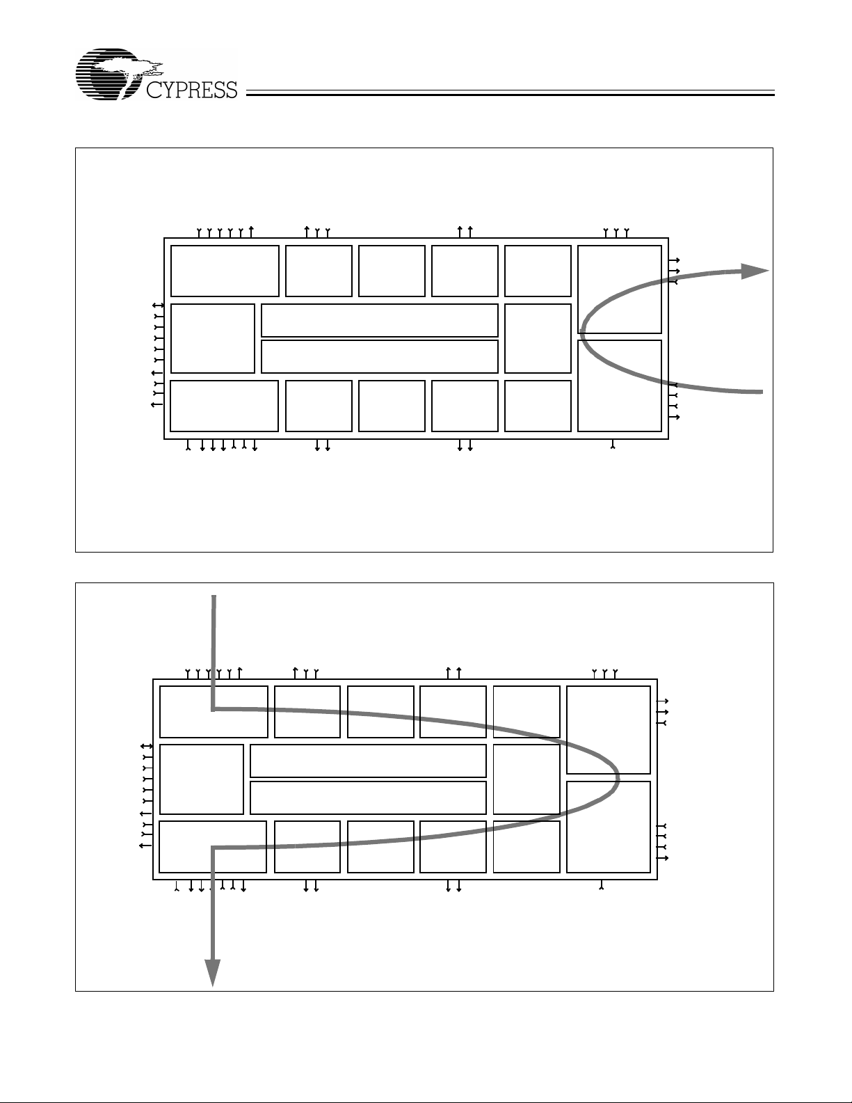
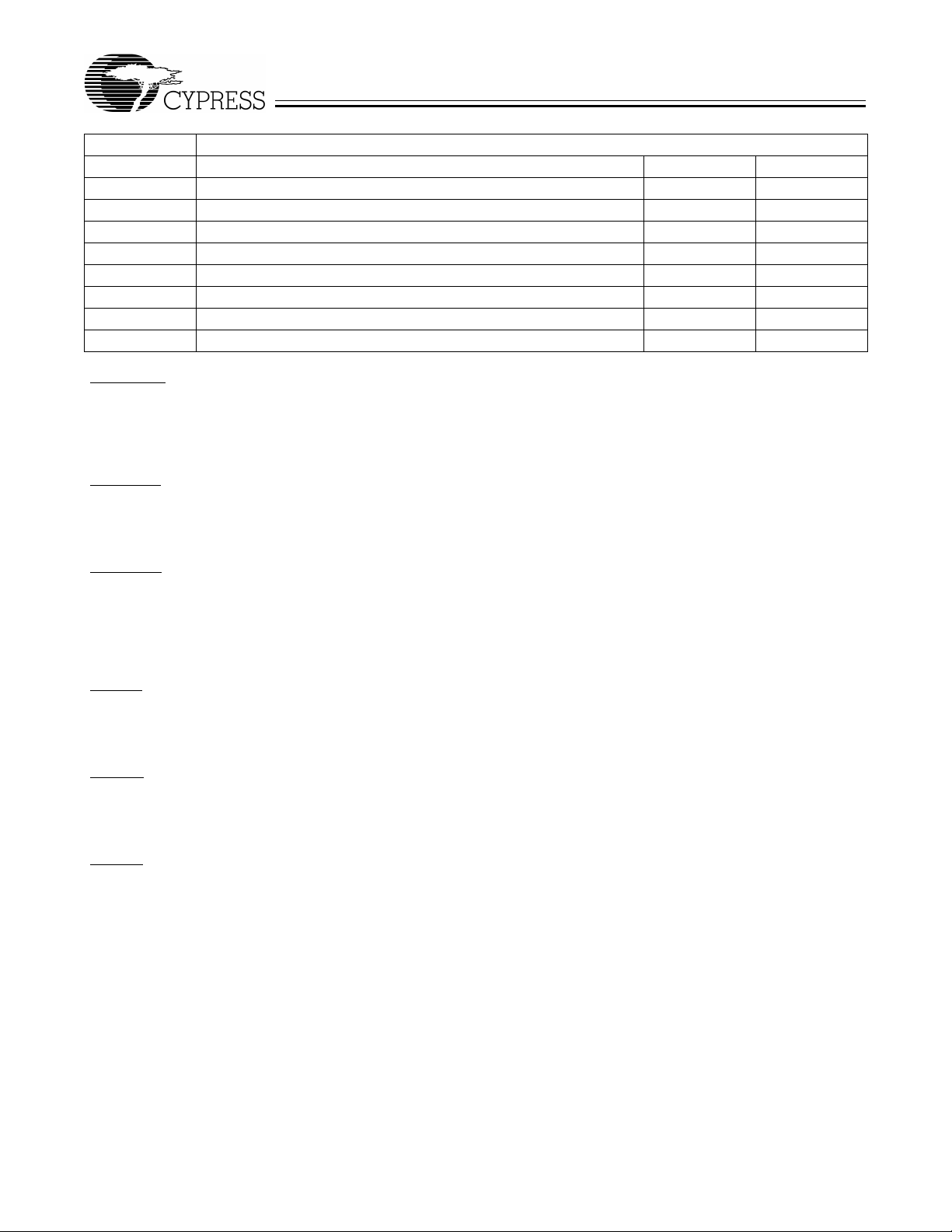
Loopback Operatio n
TDAT[7:0]
TXPRTY
PRELIMINARY
TSOC
TFCLK
TWRENB
TCA
TCP
XOFF
TGFC
TFPO
TCLK
TBYP
RATE0
RATE1
CY7C955
D[7:0]
A[7:0]
ALE
RDB
WRB
CSB
INTB
RSTB
VCLK
RALM
UTOPIA I/F
Transmit FIFO
4 Cell by 8 bit
Controller
Interface
UTOPIA I/F
Receive FIFO
4 Cell by 8 bit
TSEN
RSOC
RXPRTY
RDAT[7:0]
TDAT[7:0]
TSOC
TFCLK
TXPRTY
TWRENB
Transmit Transmit Transmit TransmitTransmit
ATM Cell
Processor
Configuration and Status
Register File
Error Monitoring
Receive Receive Receive ReceiveReceive
Processor
RCA
RFCLK
RRDENB
RCP
RGFC
Path
Overhead Overhead Overhead
PathATM Cell
Processor Processor Processor
Line Section
ProcessorProcessorProcessor
Rate
Selection
SectionLine
OverheadOverheadOverhead
RFP
RCLK
Transmit
Clock
Multiplier &
Transmit
Buffer
SONET/SDH
Clock
Recovery
RBYP
High Speed Line Loopback
RATE1
TBYP
TCA
TCP
XOFF
TGFC
TFPO
TCLK
RATE0
TXD±
TXC±
TRCLK±
ALOS±
RRCLK±
RXD±
RXDO±
7C955−10
D[7:0]
A[7:0]
ALE
RDB
WRB
CSB
INTB
RSTB
VCLK
RALM
UTOPIA I/F
Transmit FIF O
4 Cell by 8 bit
Controller
Interface
UTOPIA I/F
Receive FIFO
4 Cell by 8 bit
TSEN
RSOC
RXPRTY
RDAT[7:0]
Transmit Transmit Transmit TransmitTransmit
ATM Cell
Processo
Configuration an d S ta t us
Regis ter Fil e
Error Monitoring
Receive Receive Receive ReceiveReceive
Processor
RCA
RFCLK
RRDENB
RCP
RGFC
Path
Overhead Overhead Overhead
r
PathATM Cell
Processor Processor Processor
Line Section
RFP
RCLK
ProcessorProcessorProcessor
Rate
Selection
SectionLine
OverheadOverheadOverhead
Transmit
Clock
Multip lier &
Transmit
Buffer
SONET/SDH
Clock
Recovery
RBYP
Diagnostic Loopback
TXD±
TXC±
TRCLK±
ALOS±
RRCLK±
RXD±
RXDO±
7C955−11
16

PRELIMINARY
CY7C955
SONET Overhead Description
Signal Values Description
A1, A2 The frame ali gnment b yt es mark the begi nning of a SONET frame . The y are t ransm itted e very 125
C1 This is t he ident ificat ion b yt e f or th e STS d ata st ream. Transmit Side: In OC−1, C1 is tr ansm itted as
B1 This is the se ction bit i nterleave p arity byt e. T r ansmit Side: B1 is calcul ated using the BIP−8 algorithm
H1, H2 These are the poi nter val ue b yte. These b yt es ar e use d to l ocate the beginni ng of th e Synchro nous
H3 This is the pointer action byte. Transmit Side: H3 will be all zeroes. Receive Side: Synchronous
B2 This is the line bit interleaved parity bytes, it is used to monitor line errors. Transmit Side: B2 is
K2 This is the identity line lay er maint enance signal . Transmit Side: Bits 6, 7, and 8 of thi s byte ar e ‘110’
Z2 This is the growt h byte. It is us ed to prov ide far end bloc k error f unction usef ul for remote perf ormance
B3 This is the interleaved parity byte. Transmit Side: B3 is calcul ated over all bits of the SPE of the
C2 This is the path signal label byte for indicating the contents of the SONET payload. Transmit Side:
G1 This is the path status byte. Transmit Side: P ath remote def ect Indication (P ath RDI) together with
H4 This is the cell offset byte. Transmit Side: Thi s byte i ndicates the of fset in bytes bet ween the H4 b yte
µs in both OC−1 and OC3c speeds. Transmit Sid e: In OC−1, A1(F6
into the t ransmitted stream at the beginning of every frame. These bytes are not scrambled by the
frame synchronous SONET scrambler. Receive Side: The receiv er will search for and frame onto
the incoming A1, A2 bytes.
OH. In OC −3c, the sequence C1, C1, C1 of every fr ame is transmitted as 01
bytes are not scrambled by the fr ame-synchronous SONET scrambler. Receive side: The receiver
will ignore C1.
described in I.432. It i s inserted into the SONET data st ream bef ore the f rame syn chronous SONET
scrambl er. Receive Side: Received B1 error events are accumulated in the SBE [15:0] (Reg−12H
and Reg−13H).
Pa yload Env elope (SPE) in the SONET/SDH frame. T r ansmit si de: H1, H2 contains th e normal new
data flag (0110 ) to gether with 522 (decimal) as th e fi xed pointer value field. The concatenation
indication byte is also inserted (H1* = 93, H2* = FF). Receive Side: H1 and H2 are used to locat e
the beginni ng of the SPE. If a v alid po inter canno t be fou nd, CY7C955 will i ndicate a Los s of Po inter
State. Path AIS is detected by an all-ones pattern in H1 and H2 bytes.
Payload Data will be stuffed in the H3 byte if a negat ive stuff e vent occurs. This byte is ignored
otherwise.
calculat ed over all bits of the line overhead and the SPE cap acity of the previous frame before the
frame is being scrambled. The B2 byte itself is then placed in t he current frame before scramble.
before scramb ling when Line Remote Def ect I ndicatio n is true. Th e whole of K2 is an all -one pattern
before scrambling if Lin e AIS is inserted. Recei ve Side: Bits 6, 7, and 8 of the K2 byte are being
exami ned to determine the presence of AIS, and RDI si gnals. Access to APs registers will be
av ail a ble in future revisions .
monitoring. Transmit Side: The number of B2 errors detected in the last frame is inserted. Z2 is a
number from 0−24 indi cati ng 0 −24 errors . Recei ve Si de: A le gal (0 −24) Z2 num ber will be add ed to
the line FEBE counter.
previo us frame before s crambling and is pl aced in the current f rame befo re scramb ling. This provides
path error moni toring capability for the link. Receive Side: The val ue in B3 is accum ulated in a
register.
It’s fixed value is 13H. This indicates the payload is ATM. Receive Side: The receive si de expects
C2 to be 13H. If the data is not 13H f or 3 consecutive frames, an interrupt (if enabled) will be
generated.
the number of B3 erro rs in the last frame are inserted into G1 before scrambling f or transmission.
G1 is a number from 0−8, indicating 0−8 errors. Receive side: A legal G1 value (0−8) will be ac cumulated in the FEBE counter. Path remote defect indication is also detected through this byte.
and the first cell byte after H4. Receive Side: H4 byte is ignored.
) and A2 (28H) are inserted
H
, 02H, 03H. These
H
17

PRELIMINARY
CY7C95 5 R eg i ster Map
Address Register
Reg−00H Master Reset/Type/Identify Register
Reg−01H Master Configu ration Register
Reg−02H Master Inter rupt Register
Reg−04H Master Clock Monitor Register
Reg−05H Master Control Regis ter
Reg−06H Transmit Clock Synthesis Control Register
Reg−07H Receive Clock Synthesis Control Register
Reg−10H Receive Section Overhead Processor Control Regi ster
Reg−11H Receive Section Overhead Processor Status Register
Reg−12H LSB of the Receive Section Overhead Processor Status BIP-8 Counter
Reg−13H MSB of the Receive Sec ti on O verhead Processor Status BIP-8 Counter
Reg−14H Transmit Section Overhead Processor Control Register
Reg−15H Transmit Section Overhead Processor Control Error Insertion Register
Reg−18H Receive Line Overhead Processor Control and Status Register
Reg−19H Receive Line Overhead Processor Interrupt Enable and Status Register
Reg−1AH Line B I P −8/24 Register
Reg−1BH Line B I P −8/24 Register
Reg−1CH Line BIP−8/24 Register
Reg−1DH Line Far-End Block Error Register
Reg−1EH Line Far-End Block Error Register
Reg−1FH Line Far-End Block Error Register
Reg−20H Transmit Line Overhead Processor Register
Reg−21H Transmit Line Overhead Processor Error Insertion Register
Reg−30H Receive Path Overhead Processor Interrupt Regis ter
Reg−31H Receive Path Overhead Processor Register
Reg−33H Receive Path Overhead Processor Interrupt Enable Register
Reg−37H Receive Path Signal Label Register
Reg−38H Path BIP−8 (B3) Register
Reg−39H Path BIP−8 (B3) Register
Reg−3AH Pat h Far-End Block Error Register
Reg−3BH Pat h Far-End Block Error Register
Reg−3CH Path Far-End Block Error Register
Reg−40H Transmit Path Overhead Processor Error Insertion Register
Reg−41H Transmit Path Overhead Processor Pointer Control Register
Reg−45H Transmit Path Overhead Processor Arbitrary Payload Pointer Register
Reg−46H Transmit Path Overhead Processor Arbitrary Payload Pointer Register
Reg−48H Transmit Path Overhead Processor Path Signal Label Register
Reg−49H Transmit Path Overhead Processor Arbitrary Path Status Register
Reg−50H Receive ATM Cell Processor Control and Status Register
Reg−51H Receive ATM Cell Processor Interrupt Register
Reg−52H Receive ATM Cell Processor Match Header Pattern Register
Reg−53H Receive ATM Cell Processor Match Header Mask Register
Reg−54H Receive ATM Cell Processor Correctable HCS Error Count Register
CY7C955
18

PRELIMINARY
CY7C955
CY7C95 5 R eg i ster Map
Address Register
Reg−55H Receive ATM Cell Processor Uncorrectable HCS Error Coun t Regi ster
Reg−56H Receive ATM Cell Processor Receive Cell Counter Register
Reg−57H Receive ATM Cell Processor Receive Cell Counter Register
Reg−58H Receive ATM Cell Processor Receive Cell Counter Register
Reg−59H Receive ATM Cell Processor Receive Configuration Register
Reg−60H Transmit ATM Cell Processor Control and Status Register
Reg−61H Transmit ATM Cell Processor Unassigned Cell Header Register
Reg−62H Transmit ATM Cell Processor Unassigned Cell Payload Register
Reg−63H Transmit ATM Cell Processor FIFO Control Register
Reg−64H Transmit ATM Cell Processor Transmit Cell Counter Register
Reg−65H Transmit ATM Cell Processor Transmit Cell Counter Register
Reg−66H Transmit ATM Cell Processor Transmit Cell Counter Register
Reg−67H Transmit ATM Cell Processor Transmit Configuration Register
Reg−80H CY7C955 Test Control Register
REG−00H Master Reset / Type / Identity Register
BIT POSITION NAME READ/WRITE DEFAULT
7 RESET R/W 0
6 TYPE[2] R 0
5 TYPE[1] R 1
4 TYPE[0] R 1
3 ID[3] R 1
2 ID[2] R 1
1 ID[1] R 1
0 ID[0] R 1
(continued)
RESET
This is the master reset bit. Toggling this register has the same effect as toggling the RSTB pin, except that RSTB will reset all
registers to their default values, while writing a 1 to this register will only reset all other registers (but not itself) to their default
values. Leaving a 1 in this register puts the AX in power-down mode.
0: Normal mode.
1: Reset / Power Down Mode.
TYPE[2:0]
These bits differentiate the AX with other Cypress products.
ID[3:0]
These bits show th e revision number of the CY7C955.
19
PRELIMINARY
REG − 01H Master Configuration Register
BIT POSITION NAME READ/WRITE DEFAULT
7 Unused
6 AUTOFEBE R/W 1
5 AUTOLRDI R/W 1
4 AUTOPRDI R/W 1
3 TCAINV R/W 0
2 RCAINV R/W 0
1 RXDINV R/W 0
0 Unused
AUTOFEBE
This bit contro ls whet her Far End Block Error (FEBE) is t ransm it ted when l ine or path BIP err or is being de tected on the rec eiv e
data stream.
0: Do not generate line or path FEBE error in response to incoming li ne or path BIP error.
1: Generate line or path FEBE error in response to incoming line or pat h BIP error.
AUTOLRDI
This bit controls whether Li ne Remote Defect Indication (LRDI) is transmitted when an incoming alarm is being det ected.
0: Do not insert line RDI when line AIS , Loss of Frame (LOF) or Loss of Signal (LOS) is being detecte d.
1: Insert line RDI when line AIS, Los s of Frame (LOF) or Loss of Signal (LOS) is being detect ed.
AUTOPRDI
This bit controls whether STS Path Rem ote Def ect Indica tion (PRDI ) is transm it ted when an incomi ng alarm is being detected.
0: Do not insert STS path RDI when Loss of Signal (LO S), Loss of P oi nter (LOP), STS pat h AIS, Los s of F r ame (LOF), l ine
AIS, or Loss of Cell Delineation (LCD) is being detected.
1: Insert STS path RDI when Loss of Signal (LO S), Los s of Pointer (LOP), STS path AIS, Loss of Frame (LOF), line AIS, or
Loss of Cell Delineat ion (LCD) is being detected.
TCAINV
This bit controls the polarity of TCA.
0: TCA is active HIGH.
1: TCA is active LOW.
RCAINV
This bit controls the polarity of RCA.
0: RCA is active HIGH.
1: RCA is active LOW.
RXDINV
This bi t con tr o ls the in te r p r e ta tion of the differ ent ia l p ai r R X D.
0: Logical 1 is represe nted by RXD+ HIGH and RXD− LOW.
1: Logical 0 is represe nted by RXD+ HIGH and RXD− LOW.
CY7C955
20

PRELIMINARY
REG − 02H Master I nterrupt Register
BIT POSITION NAME READ/WRITE DEFAULT
7 TROOLI R
6 LCDI R
5 RDOOLI R
4 TACPI R
3 RACPI R
2 RPOPI R
1 RLOPI R
0 RSOPI R
TROOLI
This is the Transmit Reference Out Of Lock Interrupt. This bi t re sets when Reg−02H is being read.
1: TROOLV (Reg−06H, bit 3) has changed state since Reg−02H was last read.
0: TROOLV (Reg−06H, bit 3) has not changed state si nce Reg−02H was last read.
LCDI
This is the Loss of Cel l Delineation Int errupt. It has to be enab led by bit 7 of Reg−05H. This bit resets when Reg−02H is being
read.
1: Loss of cell delineation is entered or e xited since Reg−02H was last re ad.
0: There is no change in the loss of cell delineation state.
RDOOLI
This is the Receive Data Out Of Lock Interrupt. This bi t resets when Reg−02H is being read.
1: RDOOLV (Reg−07H, bit 3) has changed state since Reg−02H was last read.
0: RDOOLV (Reg−07H, bit 3) has not changed state since Reg−02H wa s last read.
TACPI
This is the Transmit ATM Cell Processor Interrupt. This bit resets when Reg−02H is being read. This register is a logical O R of
all the Transmit ATM Cell Processor (TACP) interrupts Reg−60H and 63H.
1: FOVRI, TSOCI, or TXPRTYI is HIGH.
0: FOVRI , TSOCI, and TXPRTYI are all LOW.
RACPI
This is the Receive ATM Cell Processor Interrupt. This bit r esets when Reg−02H is being read. This registe r i s a logical OR of
all the Receive ATM Cell Processo r (RACP) interrupts of Reg−51H.
1: OOCDI, CHCSI, or UHCSI is HIGH.
0: OOCDI, CHCSI, and UHCSI are all LOW.
RPOPI
This is the Receive Path Overhead Processor Interrupt. This bit resets when Reg−02H is being read. This register is a logical
OR of all the Receive Path Overhead Processor (RPOP) interrupts of Reg−31H.
1: PSLI, LOPI, PAISI, PRDII, BIPEI, or FEBEI is HIGH.
0: PSLI, LOPI, PAISI, PRDII, BIPEI, and FEBEI are all LOW.
RLOPI
This is the Receive Line Overhead Processor Interrupt. This bit resets when Reg−02H is being read. This register is a logical
OR of all the Receive Line Overhead Processor (RLOP) interrupts of Reg−19H.
1: FEB E I, B IP EI, LAISI, or R D II is HI GH .
0: FEBEI, BIPEI, LAISI, and RDII are all LOW.
RSOPI
This is the Receiv e Section Ov erhead Processor Inter rupt. This bit resets when Reg−02H is being read. Thi s register i s a logical
OR or all the Receive Secti on Overhead Processor (RSOP) interrupts or Reg−11H.
1: BIPEI, LOSI, LOFI, or OOFI is HIGH.
0: BIPEI, LOSI, LOFI, and OOFI are all LO W.
CY7C955
21

PRELIMINARY
REG − 04H Master Clock Monitor Register
BIT POSITION NAME READ/WRITE DEFAULT
7 RXDOD R/W 0
6 XORTXC R/W 0
5 Unused
4 Unused
3 RRCLKA R
2 TRCLKA R
1 RCLKA R
0 TCLKA R
RXDOD
This bit is used to turn off the RXDO output in case it is not needed. Thi s helps save power and reduce power supply noise.
1: RXDO output is disabled.
0: RXDO is the retimed buffered output of RXDXORTXC.
XORTXC is used to invert the defaul t-on status of the TXC output.
1: TXC is disabled if RATE0 is LOW, and TXC is a 155.52-MHz clock if RATE0 is HIGH.
0: TXC is a 51.84-MHz clock if RATE0 is LOW, and TXC is disabled if RATE0 is HIGH.
RRCLKA
This bit can be read to check for RRCLK transitions ; when HIGH, thi s bit stays HIGH until Reg −04H is being read.
1: RRCLK+ has a LOW to HIGH transiti on since this register was last read.
0: RRCLK+ has no LOW to HIGH transitions since this regis ter was last read.
TRCLKA
This bit can be read to check for TRCLK transitions ; when HI GH, thi s bit stays HIGH until Reg−04H is being read.
1: TRCLK+ has a LOW to HIGH transition since this register was last read.
0: TRCLK+ has no LOW to HIGH transitions since this register was last read.
RCLKA
This bit can be read to check for RCLK transitions; when HIGH, thi s bit stays HIGH until Reg −04H is being read.
1: RCLK has a LOW to HIGH transit ion since this regist er was last read.
0: RCLK has no LOW to HIGH transitions since this register was last read.
TCLKA
This bit can be read to check for TCLK transitions; when HIGH, this bit stays HIGH unti l Reg−04H is being read.
1: TRCLK+ has a LOW to HIGH transition since this register was last read.
0: TRCLK+ has no LOW to HIGH transitions since this register was last read.
CY7C955
22

PRELIMINARY
REG − 05H Master Control Register
BIT POSITION NAME READ/WRITE DEFAULT
7 LCDE R/W 0
6 LCDV R
5 FIXPTR R/W 1
4 Unused
3 Unused
2 LLE R/W 0
1 DLE R/W 0
0 LOOPT R/W 0
LCDE
This bit enables a change in the Loss of Cell Delineation state to generate an interrupt on pin INTB.
0: INTB will not be affected by a transition in LCDV (Reg−05H, bit 6).
1: INTB will go LOW when there is a transition in LCDV (Reg−05H, bit 6).
LCDV
This bit shows the present loss of cell del ineation state of the Receive ATM Cell overhead Processo r (RACP).
0: RACP is in SYNC state f or l onger than 4 ms.
1: RACP is out of cell delineation for more than 4 ms and there are no detected LOS, LOP, Path AIS, and Line AIS.
FIXPTR
This bit controls the operation of the transmit payload pointer adjustment function.
0: The setting in Reg−41H can con trol the payload point er adjustment operat ions.
1: The transmit payload pointer is fixed at 522.
LLE
This bit controls the li ne loop-back path of the CY7C955; DLE and LLE cannot be both set to 1.
0: Normal operation.
1: RXD+ and RXD− are connected to TXD+ and TXD− internally.
DLE
This bit controls the diagnostic loop-back path of the CY7C955; DLE and LLE cannot be both set to 1.
0: Normal operation.
1: The transmitted data steam is being looped bac k to the received data stream.
LOOPT
This bit enables loop timing.
0: The transmit ted data stream derives its cloc k from TRCLK. The cloc k to use depends on the setting of TREFSEL
(Reg−06H, bit 0) and on the level of pins TBYP and RATE0.
1: The transmitted dat a stream derives its clock from RRCLK if the clock and data recovery function of the receiver is not
active and f rom RXD if the cl ock and data recovery function is activ e. Again, the clock to use in RRCLK depends on
the setting of RREFSEL (Reg−07H), RBYP, and RATE0.
CY7C955
23

PRELIMINARY
REG − 06H Transmit Clock Synthesis Contr ol Regi ster
BIT POSITION NAME READ/WRITE DEFAULT
7 Unused
6 Unused
5 Unused
4 Unused
3 TROOLV R
2 Unused
1 TROOLE R/W 0
0 TREFSEL R/W 0
TROOLV
This bit is the Transmit Reference Out Of Lock Status register.
0: The divided-do wn synthesized tr ansmit clock is within 2930 ppm of TRCLK or RRCLK (in loop ti ming mode).
1: The divided-do w n synthesized transmit clock is not with in 2930 ppm of TRCLK or RRCLK (in loop timing mode).
TROOLE
This bit is the Transmit Reference Out Of Lock Interrupt Enable register.
0: INTB, the interrupt pin, will not be aff ected by transmit out of lock.
1: INTB, the interrupt pin, will pull LOW when there is a state change of TROOLV.
TREFSEL
This bit is the Transmit Reference Select. This bit is ignored in transmit bypass mode (TBYP = 1).
0: TRCLK expects a 19.44-MHz reference clock. If RATE0 is HIGH (155.52 Mbps, STS−3c/STM−1), the transmit PLL will
multiply the TRCLK frequency by 8 times. If RATE0 is LOW (51.84 Mbps, STS−1), the transmit PLL will multiply the
TRCLK frequency by 8/ 3 times to clock the transmitter .
1: TRCLK expects a 6.48-MHz reference clock. If RATE0 is HIGH (155.52 Mbps, STS−3c/STM−1), the transmit PLL will
multiply the TRCLK frequency by 24 times. If RATE0 is LOW (51.84 Mbps, STS−1), the t ransm it P LL will multi ply the
TRCLK frequency by 8 tim es to clock the transmit ter.
CY7C955
24

PRELIMINARY
REG − 07H Recei ve Clock Synthesis Control Regi ster
BIT POSITION NAME READ/WRITE DEFAULT
7 Unused
6 Unused
5 Unused
4 Unused
3 RROOLV R
2 Unused
1 RROOLE R/W 0
0 RREFSEL R/W 0
RROOLV
This bit is the Receive Reference Out Of Lock Status register.
0: The divided-down reco vered clock is within 2930 ppm of RRCLK, and there is at least one tran sition on RXD during
the last 80 bit-periods.
1: The divided-down recovered clock is not within 2930 ppm of RRCLK, or there are no trans it ions on RXD within the last
80 bit-periods.
RROOLE
This bit is the Receive Reference Out Of Lock Interrupt Enabl e regi ster.
0: INTB, the interrupt pin, will not be aff ected by receiv er out of lock.
1: INTB, the interrupt pin, will go LOW when there is a state change of RROOLV.
RREFSEL
This bit is the Receiver Reference Select. This bit is ignored in receiver bypass mode (RBYP = 1).
0: RRCLK expects a 19.44-MHz reference clock. If RATE0 is HIGH (155.52 Mbps, STS−3c/STM−1), the recovered clock
is divided down 8 times before comparing with RRCLK. If RATE0 is LOW (51.84 Mbps, STS−1), the recovered clock is
divided down 3/8 times before comparing with RRCLK.
1: RRCLK expects a 6.480-MHz reference clock. If RATE0 is HIGH (155.52 Mbps, STS−3c/STM−1), the recovered clock
is divided down 24 times before comparing wit h RRCLK. If RATE0 is LOW (51.84 Mbps , STS−1), the recovered clock is
divided down 8 times before comparing with RRCLK.
CY7C955
25

PRELIMINARY
REG − 10H Recei ve Section Overhead Processor Cont rol Register
BIT POSITION NAME READ/WRITE DEFAULT
7 Unused
6 DDS R/W 0
5 FOOF W 0
4 Unused
3 BIPEE R/W 0
2 LOSE R/W 0
1 LOFE R/W 0
0 OOFE R/W 0
DDS
This bit controls whether SONET descrambling is done on the receive data stream.
0: Descramb li ng is performed.
1: Descramb li ng is not performed.
FOOF
This bit can be used to manually put the Receive Secti on Overhead Processor out of frame.
0: No action.
1: The Receive Section Overhead Proce ssor will detect an out of frame alarm at the next frame boundary.
BIPEE
This bit controls whether a section BIP−8 error (B1) gener ates an interrupt.
0: The interrupt pin, INTB, is not affected by section BIP−8 errors .
1: The interrupt pin, INTB, will go LOW upon receivi ng a section BIP−8 error.
LOSE
This bit controls whether a Loss of Signal alarm generates an interrupt.
0: The interrupt pin, INTB, is not affected by the loss of signal alarm.
1: The interrupt pin, INTB, will go LOW upon receiving a loss of signal alarm.
LOFE
This bit controls whether a Loss of Frame al arm generates an interrupt.
0: The interrupt pin, INTB, is not affected by the lo ss of frame alarm.
1: The interrupt pin, INTB, will go LOW upon receivi ng a loss of frame alarm.
OOFE
This bit controls whether an Out of Frame alarm generates an interrupt.
0: The interrupt pin, INTB, is not affected by the out of frame alarm.
1: The interrupt pin, INTB, will go LOW upon receiving an out of frame alarm.
CY7C955
26

PRELIMINARY
REG − 11H Recei ve Section Overhead Processor Sta tus Register
BIT POSITION NAME READ/WRITE DEFAULT
7 Unused
6 BIPEI R
5 LOSI R
4 LOFI R
3 OOFI R
2 LOSV R
1 LOFV R
0 OOFV R
BIPEI
This is the section BIP −8 interrupt bit. This bit resets when Reg−11H is being read.
0: No section BIP−8 error is det ected since Reg−11H was last read .
1: Section BIP−8 error is det ected since Reg−11H was last read.
LOSI
This is the Loss of Signal (LOS) interrupt bit. This bit resets when Reg−11H is being read.
0: No change in the LOS status.
1: There is a change in the LOS status since Reg−11H was last read.
LOFI
This is the Loss of Frame (LOF) interrupt bit. This bit resets when Reg−11H is being read.
0: No change in the LOF status .
1: There is a change in the LOF status since Reg−11H was last read.
OOFI
This is the Out of Frame (OOF) interrupt bit. This bit resets when Reg−11H is being read.
0: No change in the OOF status.
1: There is a change in the OOF status since Reg−11H was last read.
LOSV
This bit shows the Loss of Signal (LOS) status of the CY7C955.
0: The Receive Section Overhead Processor is not in a loss of signal st ate.
1: The Receive Section Overhead Processor is in a loss of signal state.
LOFV
This bit shows the Loss of Frame (LOF) status of the CY7C955.
0: The Receive Section Overhead Processor is not in a Loss of Frame state.
1: The Receive Section Overhead Processor is in a Loss of Frame state. LOF is declared when OOF has lasted for more
than 3 ms. LOFV stays HIGH until the Receive Sect ion Overhead Processor is in frame for more than 3 ms.
OOFV
This bit shows the Out of Frame (OOF) status of the CY7C955.
0: The Receive Section Overhead Processor is in frame.
1: The Receive Section Overhead Processor is in an out of frame state.
CY7C955
27

PRELIMINARY
REG − 12H LSB of the Receive Section Overhead Processor Status BIP−8 coun ter
BIT POSITION NAME READ/WRITE DEFAULT
7 SBE[7] R 0
6 SBE[6] R 0
5 SBE[5] R 0
4 SBE[4] R 0
3 SBE[3] R 0
2 SBE[2] R 0
1 SBE[1] R 0
0 SBE[0] R 0
SBE[15:0]
Reg−12H and Re g−13H wil l l oad th e n umber o f BIP−8 error s from an internal counter app rox imately 1 µs after a write oper ation
is done to Reg−12H, Reg−13H, or Reg−00H. At that time (1 µs after the write operation), these two registers are updated and
the in ternal BI P −8 err or coun ter is r eset t o zer o t o begin another ro und of er ror a ccum ulati on. Readi ng Reg−1 2H and Reg−13H
after the write yields the number of BIP−8 (B1) errors accumulated since the counter was last written to, if overflow has not
occurred.
REG − 13H MSB of the Receive Section Overhead Processor St atus BIP−8 counter
BIT POSITION NAME READ/WRITE DEFAULT
7 SBE[15] R 0
6 SBE[14] R 0
5 SBE[13] R 0
4 SBE[12] R 0
3 SBE[11] R 0
2 SBE[10] R 0
1 SBE[9] R 0
0 SBE[8] R 0
CY7C955
SBE[15:0]
Reg−12H and Re g−13H wil l l oad th e n umber o f BIP−8 error s from an internal counter app rox imately 1 µs after a write oper ation
is done to Reg−12H, Reg−13H, or Reg−00H. At that time (1 µs after the write operation), these two registers are updated and
the in ternal BI P −8 err or coun ter is r eset t o zer o t o begin another ro und of er ror a ccum ulati on. Readi ng Reg−1 2H and Reg−13H
after the write yields the number of BIP−8 (B1) errors accumulated since the counter was last written to if overflow has not
occurred.
28

PRELIMINARY
REG − 14H Transmit Section Overhead Processor Cont rol Register
BIT POSITION NAME READ/WRITE DEFAULT
7 Unused
6 DS R/W 0
5 Unused
4 Unused
3 Unused
2 Unused
1 Unused
0 LAIS R/W 0
DS
This bit controls whether SONET scrambling is done to the transmit data stream.
0: Scrambling is performed.
1: Scrambling is not performed.
LAIS
This bit controls whether line Alarm Indication Signal (AIS) is being inserted into the transmit data stream.
1: All bits in the SONET frame (excluding the section overhead) are converted to a 1 prior to SONET scrambling. This
operation begins immediately at the next frame boundary.
0: No line AIS is transmitt ed.
CY7C955
REG − 15H Transmit Section Overhead Processor Error Insertion Register
BIT POSITION NAME READ/WRITE DEFAULT
7 Unused
6 Unused
5 Unused
4 Unused
3 Unused
2 DLOS R/W 0
1 DBIP8 R/W 0
0 DFP R/W 0
DLOS
This bit generates a continuous loss of signal error in the transmit dat a stream.
0: Normal operation.
1: TXD transmits all zeros.
DBIP8
This bit generates a continuous section BIP−8 (B1) error in the transmit data stream.
0: Normal operation.
1: B1 byte is inverted.
DFP
This bit generates a fr am ing byte error in the transmit data stream.
0: Normal operation.
1: The most significant bit of the section overhead framing byte is conver ted from 1 to 0. In other words, F6H becomes H
in the first A1 byte of the section overhead.
29

PRELIMINARY
REG − 18H Receive LIne Overhead Processor Control and Status Register
BIT POSITION NAME READ/WRITE DEFAULT
7 BIPWORD R/W 0
6 Unused
5 Unused
4 Unused
3 Unused
2 Unused
1 LAISV R 0
0 RDIV R 0
BIPWORD
This bit controls how many times a B2 error is recorded.
0: The B2 error counter increments only once per frame on receiving B2 bit-errors.
1: The B2 error counter increments once for every bit error represented in the B2 word. Note that in STS−3c, there could
be at most 24 B2 bit-errors per frame, and in STS−1, there could be, at most, 8 B2 bit-erro rs per frame.
LAISV
This bit is the Line Alarm Indicati on Signal (LAIS) status regist er.
0: No Line AIS detected.
1: Line AIS has been detected. Line AIS is triggered by LOS or LOF.
RDIV
This bit is the Remote Def ect Indication status register.
0: No remote defect indication (RDI) detected .
1: Remote defect indication (RDI) has been detected.
CY7C955
30

PRELIMINARY
REG − 19H Recei ve Line Overhead Processor Inte rrupt Enable and Status Register
BIT POSITION NAME READ/WRITE DEFAULT
7 FEBEE R/W 0
6 BIPEE R/W 0
5 LAISE R/W 0
4 RDIE R/W 0
3 FEBEI R
2 BIPEI R
1 LAISI R
0 RDII R
FEBEE
This bit controls whether line far end block error generates an interrupt by asserting INTB LOW.
0: Line far- end block error will not generate an interrupt.
1: Line far- end block error will generate an inte rrupt.
BIPEE
This bit controls whether BIP−24 (B2) error generates an interrupt by asserting INTB LOW.
0: BIP−24 error will not generate an interrupt.
1: BIP−24 error will generate an interrupt.
LAISE
This bit controls whether line alarm indication signa l (L AIS) error generates an interrupt by asserting INTB LOW.
0: LAIS error will not generate an interrupt.
1: LAIS error will generate an interrupt.
RDIE
This bit controls whether a remote defect indication alarm det ection generates an interrupt by asserting INTB LOW.
0: A change in the RDIV state (Reg−18H, bit 0) will not generate an interrupt.
1: A change in the RDIV state (Reg−18H, bit 0) will generate an interrupt.
FEBEI
This is the line f ar- end block error interrupt bit. This bit reset s when Reg−19H is being read.
0: No line far -end block error has been detected since Reg−19H was last read.
1: Line far- end block error has been detected since Reg−19H was last read.
BIPEI
This is the section BIP −24 (B2) interrupt bit. This bit resets when Reg−19H is being read.
0: No line BIP−24 (B2) error has been detected since Reg−19H was last re ad.
1: Line BIP−24 (B2) error has been detected since Reg−19H was last read.
LAISI
This is the Li ne Alarm Indication Signal (LAIS) interrupt bit. This bit resets when Reg−19H is bei ng read.
0: No LAIS has been detected si nce Reg−19H was last read.
1: LAIS has been detected since Reg−19H was last read.
RDII
This is the Remote Defect Indication (RDI) inte rrupt bit . This bit resets when Reg−19H is being read.
0: No line remote def ect indication has been detected since Reg−19H was last read.
1: Line remote defect indication has been detected since Reg−19H was last read.
CY7C955
31

PRELIMINARY
REG − 1AH Line BIP−8/24 Register
BIT POSITION NAME READ/WRITE DEFAULT
7 LBE[7] R 0
6 LBE[6] R 0
5 LBE[5] R 0
4 LBE[4] R 0
3 LBE[3] R 0
2 LBE[2] R 0
1 LBE[1] R 0
0 LBE[0] R 0
LBE[19:0]
Reg−1AH to Reg−1CH will be loaded with the number of BIP−8/24 (B2) err ors f rom a n int ernal cou nter appr oxi mate ly 1 µs af ter
a write operation is done to Reg−1AH, Reg−1BH, Reg−1CH, Reg−1DH, Reg−1EH, Reg−1FH, or Reg−00H. At that time (1 µs
after the write operation), these three registers are updated and the internal BIP−8/24 error counter reset to zer o to begin
another round of error acc umulation. Reading Reg −1AH, Reg−1BH, and Reg−1CH after the write yields the number of BIP−8/24
(B2) errors accumulated since the counter was last reset, if overflow has not occurred.
REG − 1BH Line BIP−8/24 Register
BIT POSITION NAME READ/WRITE DEFAULT
7 LBE[15] R 0
6 LBE[14] R 0
5 LBE[13] R 0
4 LBE[12] R 0
3 LBE[11] R 0
2 LBE[10] R 0
1 LBE[9] R 0
0 LBE[8] R 0
CY7C955
LBE[19:0]
Reg−1AH to Reg−1CH will be loaded with the number of BIP−8/24 (B2) err ors f rom a n int ernal cou nter appr oxi mate ly 1 µs af ter
a write operation is done to Reg−1AH, Reg−1BH, Reg−1CH, Reg−1DH, Reg−1EH, Reg−1FH, or Reg−00H. At that time (1 µs
after the write operation), these three registers are updated and the internal BIP−8/24 error counter is reset to zero to begin
another round of error acc umulation. Reading Reg −1AH, Reg−1BH, and Reg−1CH after the write yields the number of BIP−8/24
(B2) errors accumulated since the counter was last reset, if overflow has not occurred.
32

PRELIMINARY
REG − 1CH Line BIP−8/24 Register
BIT POSITION NAME READ/WRITE DEFAULT
7 Unused
6 Unused
5 Unused
4 Unused
3 LBE[19] R 0
2 LBE[18] R 0
1 LBE[17] R 0
0 LBE[16] R 0
LBE[19:0]
Reg−1AH to Reg−1CH will be loaded with the number of BIP−8/24 (B2) err ors f rom a n int ernal cou nter appr oxi mate ly 1 µs af ter
a write operation is done to Reg−1AH, Reg−1BH, Reg−1CH, Reg−1DH, Reg−1EH, Reg−1FH, or Reg−00H. At that time (1 µs
after the write operation), these three registers are updated and the internal BIP−8/24 error counter is reset to zero to begin
another round of error acc umulation. Reading Reg −1AH, Reg−1BH, and Reg−1CH after the write yields the number of BIP−8/24
(B2) errors accumulated since the counter was last reset, if overflow has not occurred.
REG − 1DH Line Far End Block Error Register
BIT POSITION NAME READ/WRITE DEFAULT
7 LFE[7] R 0
6 LFE[6] R 0
5 LFE[5] R 0
4 LFE[4] R 0
3 LFE[3] R 0
2 LFE[2] R 0
1 LFE[1] R 0
0 LFE[0] R 0
CY7C955
LFE[19:0]
Reg−1DH, Reg−1EH, and Reg−1FH will be loaded with the number of line FEBE (Z2) errors from an internal counter appr oximately 1 µs after a write operation is done to Reg−1AH, Reg−1BH, Reg−1CH, Reg−1DH, Reg−1EH, Reg−1FH, or Reg−00H.
At that time (1 µs after the write operatio n), these three registers are updated and the internal line FEBE error counter is reset
to zero to begin another round of error accumulation. Reading Reg−1DH, Reg−1EH, and Reg−1FH after the write yields the
number of line FEBE (Z2) errors accumulated since the count er was last reset, if overflow has not occurred.
33

PRELIMINARY
REG − 1EH Line Far End Block Error Register
BIT POSITION NAME READ/WRITE DEFAULT
7 LFE[15] R 0
6 LFE[14] R 0
5 LFE[13] R 0
4 LFE[12] R 0
3 LFE[11] R 0
2 LFE[10] R 0
1 LFE[9] R 0
0 LFE[8] R 0
LFE[19:0]
Reg−1DH, Reg−1EH, and Reg−1FH will be loaded with the number of line FEBE (Z2) errors from an internal counter appr oximately 1 µs after a write operation is done to Reg−1AH, Reg−1BH, Reg−1CH, Reg−1DH, Reg−1EH, Reg−1FH, or Reg−00H.
At that time (1 µs a fter the write o per ation ), t hese thr ee regi ster s are upd ate d and the in ternal li ne FEBE err or coun ter are r eset
to zero to begin another round of error accumulation. Reading Reg−1DH, Reg−1EH, and Reg−1FH after the write yields the
number of line FEBE (Z2) errors accumulated since the count er was last reset, if overflow has not occurred.
REG − 1FH Line Far End Block Error Register
BIT POSITION NAME READ/WRITE DEFAULT
7 Unused R 0
6 Unused R 0
5 Unused R 0
4 Unused R 0
3 LFE[19] R 0
2 LFE[18] R 0
1 LFE[17] R 0
0 LFE[16] R 0
CY7C955
LFE[19:0]
Reg−1DH, Reg−1EH, and Reg−1FH will be loaded with the number of line FEBE (Z2) errors from an internal counter appr oximately 1 µs after a write operation is done to Reg−1AH, Reg−1BH, Reg−1CH, Reg−1DH, Reg−1EH, Reg−1FH, or Reg−00H.
At that time ( 1 µs after the write opera tion) , these t hree r egist ers ar e u pdated and t he in ternal l ine F EBE error c ounter are r eset
to zero to begin another round of error accumulation. Reading Reg−1DH, Reg−1EH, and Reg−1FH after the write yields the
number of line FEBE (Z2) errors accumulated since the count er was last reset, if overflow has not occurred.
34

PRELIMINARY
REG − 20H Transmit Line Overhead Processor Register
BIT POSITION NAME READ/WRITE DEFAULT
7 Unused
6 Unused
5 Unused
4 Unused
3 Unused
2 Unused
1 Unused
0 RDI R/W 0
RDI
This bit controls whether line far end receive failure (RDI) is being inserted into the tran sm it data stream.
0: Transmit 000 in bits 6, 7, and 8 of K2.
1: Transmit 110 in bits 6, 7, and 8 of K2.
REG − 21H Transmit Line Overhead Processor Error Insertion Register
BIT POSITION NAME READ/WRITE DEFAULT
7 Unused
6 Unused
5 Unused
4 Unused
3 Unused
2 Unused
1 Unused
0 DBIP R/W 0
CY7C955
DBIP
This bit generates a continuous line BIP−8/24 (B2) error in the transm it data stream.
0: Normal operation.
1: Insert BIP8/24 (B2) error by inverting the B2 byte.
35

PRELIMINARY
REG − 30H Recei ve Path Overhead Processor Interrupt Register
BIT POSITION NAME READ/WRITE DEFAULT
7 Unused
6 Unused
5 LOP R
4 Unused
3 PAIS R
2 PRDI R
1 Unused
0 Unused
LOP
This bit is the Loss of Pointer (LOP) alarm regi ster.
0: N o lo s s of pointer al a rm det ected.
1: Loss of pointer alarm detec ted.
PAIS
This bit is the path Alarm Indication Signal (AIS) register.
0: No path alarm indication signal detected.
1: Path alarm indication signal detected.
PRDI
This bit is the path Far-End Receive Failure (RDI) alarm register.
0: No path far- end receive fail ure (RDI) alarm detected.
1: Path far-end receive failure (RDI) alarm detected.
CY7C955
36

PRELIMINARY
REG − 31H Recei ve Path Overhead Processor Register
BIT POSITION NAME READ/WRITE DEFAULT
7 PSLI R
6 Unused
5 LOPI R
4 Unused
3 PAISI R
2 PRDII R
1 BIPEI R
0 FEBEI R
PSLI
This is the Path Signal Label (PSL) register interrupt bit. This bit resets when Reg−31H is being read.
0: No change in the path signal label since Reg−31H was last read.
1: There is a change in the path si gnal label since Reg−31H was last rea d.
LOPI
This is the Loss of Pointer (LOP) interrupt bit . This bit resets when Reg−31H is being read.
0: No change in the loss of pointer state since Reg−31H was last read.
1: There is a change in the loss of pointer state since Reg−31H was last read.
PAISI
This is the path Alarm Indication Signal (AIS) interrupt bit. This bit resets when Reg−31H is being read.
0: No change in the path alarm indication signal since Reg−31H was last read.
1: There is a change in the path al arm indi cation signal since Reg−31H wa s last read.
PRDII
This is the path Far-End Receive Failure (RDI) alarm interrupt bit. This bit resets when Reg−31H is being r ead.
0: No change in the path far-end receive failure alarm since Reg−31H was last read.
1: There is a change in the path f ar-end recei ve failure alarm since Reg−31H was last read.
BIPEI
This is the BIP−8 (B3) error interrupt bit. This bit resets when Reg −3 1H is being read.
0: No BIP−8 (B3) error detected since Reg−31H was last re ad.
1: BIP−8 (B3) error has been detected since Reg−31H was last rea d.
FEBEI
This is the path Far -End Block Error (FEBE) interrupt bit. This bit resets when Reg−31H is being read.
0: No path far- end block error detected since Reg−31H was last read.
1: Pat h far-end bloc k error has been detected since Reg−31H was last read.
CY7C955
37

PRELIMINARY
REG − 33H Recei ve Path Overhead Processor Interrupt Enable Register
BIT POSITION NAME READ/WRITE DEFAULT
7 PSLE R/W 0
6 Unused
5 LOPE R/W 0
4 Unused
3 PAISE R/W 0
2 PRDIE R/W 0
1 BIPEE R/W 0
0 FEBEE R/W 0
PSLE
This bit controls whether a change in the Path Signal Label (PSL) generates an interrupt by asserting INTB LOW.
0: A change in the path signal l abel (PSL) will not generate an in ter rupt.
1: An interrupt wil l be generated if more than two consecutive non-13H C3 bytes are being detec ted i n the path overhead.
LOPE
This bit controls whether a loss of poi nter generates an interrupt by asserting INTB LOW.
0: A change in the loss of point er state will not generate an in terrupt.
1: A change in the loss of point er state will generate an int errupt.
PAISE
This bit controls whether Path Alarm Indication Signal (PAIS) error generates an interrupt by asserting INTB LOW.
0: PAIS error will not generate an interrupt.
1: PAIS err o r w ill g e nera t e a n inte r rupt.
PRDIE
This bit controls whether a path Remote Defect Indication (RDI) generates an interrupt by asserting INTB LOW.
0: A change in the path remote defect indication state will not generate an interrupt.
1: A change in the path remote defect indication state will generate an int errupt.
BIPEE
This bit controls whether BIP−8 (B3) error generates an interrupt by asserting INTB LOW.
0: BIP−8 (B3) error will not generate an interrupt.
1: BIP−8 (B3) error will generate an interrupt.
FEBEE
This bit controls whether line far end block error generates an interrupt by asserting INTB LOW.
0: Line far- end block error will not generate an interrupt.
1: Line far- end block error will generate an inte rrupt.
CY7C955
38

PRELIMINARY
REG − 37H Receive Path Signal Label Register
BIT POSITION NAME READ/WRITE DEFAULT
7 PSL[7] R
6 PSL[6] R
5 PSL[5] R
4 PSL[4] R
3 PSL[3] R
2 PSL[2] R
1 PSL[1] R
0 PSL[0] R
PSL[7:0]
This is the path signal label (C2) register byte. This register is either 13H or the first non-13H value detected in the recei ved
SONET data stream.
REG − 38H Path BIP−8 (B3) Register
BIT POSITION NAME READ/WRITE DEFAULT
7 PBE[7] R 0
6 PBE[6] R 0
5 PBE[5] R 0
4 PBE[4] R 0
3 PBE[3] R 0
2 PBE[2] R 0
1 PBE[1] R 0
0 PBE[0] R 0
CY7C955
PBE[15:0]
Reg−38H and Reg−39H will be loaded with the numbe r of path BIP−8 (B3) errors from an internal counter approximately 1 µs
after a write operation is done to Reg−38H, Reg−39H, Reg−3AH, Reg−3BH, or Reg−00H. At that time (1 µs after th e wr ite
operation), these three registers are updated and the internal BIP−8 (B3) error counter is reset to zero to begin another round
of error accumulation. Reading Reg−38H and Reg−39H after the write yields the number of BIP−8 (B3) errors accumulated
since the counter w as last reset, if overflow has not occurr ed.
39

PRELIMINARY
REG − 39H Path BIP−8 (B3) Register
BIT POSITION NAME READ/WRITE DEFAULT
7 PBE[15] R 0
6 PBE[14] R 0
5 PBE[13] R 0
4 PBE[12] R 0
3 PBE[11] R 0
2 PBE[10] R 0
1 PBE[9] R 0
0 PBE[8] R 0
PBE[15:0]
Reg−38H and Reg−39H will be loaded with the numbe r of path BIP−8 (B3) errors from an internal counter approximately 1 µs
after a write operation is done to Reg−38H, Reg−39H, Reg−3AH, Reg−3BH, or Reg−00H. At that time (1 µs after th e wr ite
operation), these three registers are updated and the internal BIP−8 (B3) error counter is reset to zero to begin another round
of error accumulation. Reading Reg−38H and Reg−39H after the write yields the number of BIP−8 (B3) errors accumulated
since the counter w as last reset, if overflow has not occurr ed.
REG − 3AH Path Far-End Block Error Register
BIT POSITION NAME READ/WRITE DEFAULT
7 PFE[7] R 0
6 PFE[6] R 0
5 PFE[5] R 0
4 PFE[4] R 0
3 PFE[3] R 0
2 PFE[2] R 0
1 PFE[1] R 0
0 PFE[0] R 0
CY7C955
PFE[15:0]
Reg−3AH and Reg−3BH will be loaded with the number of pat h FEBE (G1) errors from an internal counter approximately 1 µs
after a write operation is done to Reg−38H, Reg−39H, Reg−3AH, Reg−3BH, or Reg−00H. At that time (1 µs after th e wr ite
operation), these three registers are updated and the internal path FEBE error counter is reset to zero to begi n another round
of error accumul ation. Reading Reg−3AH and Reg−3BH afte r the write yields the number of path FEBE (G1) errors accumulated
since the counter w as last reset, if overflow has not occurr ed.
40

PRELIMINARY
REG − 3BH Pat h Fa r E n d Blo ck E rro r R e g is ter
BIT POSITION NAME READ/WRITE DEFAULT
7 PFE[15] R 0
6 PFE[14] R 0
5 PFE[13] R 0
4 PFE[12] R 0
3 PFE[11] R 0
2 PFE[10] R 0
1 PFE[9] R 0
0 PFE[8] R 0
PFE[15:0]
Reg−3AH and Reg−3BH will be loaded with the number of pat h FEBE (G1) errors from an internal counter approximately 1 µs
after a write operation is done to Reg−38H, Reg−39H, Reg−3AH, Reg−3BH, or Reg−00H. At that time (1 µs after th e wr ite
operation), these three registers are update and the internal path FEBE error counter is reset to zero to begin another round
of error accumul ation. Reading Reg−3AH and Reg−3BH afte r the write yields the number of path FEBE (G1) errors accumulated
since the counter w as last reset, if overflow has not occurr ed.
REG − 3DH Path Far-End Block Error Register
BIT POSITION NAME READ/WRITE DEFAULT
7 Unused
6 Unused
5 BLKBIP R/W 0
4 Unused
3 Unused
2 Unused
1 Unused
0 Unused
CY7C955
BLKBIP
This bit controls how path BIP−8 (B3) errors are accumulated.
0: BIP−8 (B3) errors are accumu lated and reported in a bit basis.
1: BIP−8 (B3) errors are acc umul ated and re ported in a bloc k bas is. Only one BIP−8 error is reported to the upstr eam pat h
ev en if mo re th an one path BIP−8 (B3) errors are detecte d.
41

PRELIMINARY
REG − 40H Transmit Path Overhead Processor Error Insertion Register
BIT POSITION NAME READ/WRITE DEFAULT
7 Unused
6 Unused
5 Unused
4 Unused
3 Unused
2 Unused
1 DB3 R/W 0
0 PAIS R/W 0
DB3
This bit generates a path BIP−8 error in the tr ansmit data stream.
0: Normal operation.
1: The path BIP−8 (B3) byte is inverted, eight BIP−8 (B3) errors are thus generated per frame PAIS.
PAIS
This bit generates a path Alarm Indication Signal (AIS) in the transmit data stream.
0: Normal operation.
1: The whole synchronous payload envelope (SPE) together with the H1, H2, and H3 bytes are converted to 1 before
scrambling.
CY7C955
42

PRELIMINARY
REG − 41H Transmit Path Overhead Processor Poi nter Control Register
BIT POSITION NAME READ/WRITE DEFAULT
7 Unused
6 FTPTR R/W 0
5 SOS R/W 0
4 PLD R/W 0
3 NDF R/W 0
2 NSE R/W 0
1 PSE R/W 0
0 Unused
FTPTR
This bit en ables the insertion of the arbi trary paylo ad pointer value int o the last 10 bits of H1, H2. The NDF flag is not automatically changed b y thi s operation.
0: Normal operation.
1: The bits contained in Arbitrary Pointer Register (APTR[ 9:0]) are inserted i nto H1 and H2 of the transmitted data stream.
This bit is provi ded for creat ing pointer byte errors to diagnose the downstream system.
SOS
This is the stuff opportunity spacing bit which controls how often stuff events can occur.
0: Stuff event can occur in every other frame. Insertion of positive pointer movement or negative pointer movement can be
done through writing to NSE and PSE (bit 2 and 1 of Reg−41H)
1: Stuff ev ent can occur onl y once in every f our frames . Insertion of positiv e pointer mov ement or negative poi nter mov ement
can be done t hrough writing to NSE and PSE (bit 2 and 1 of Reg−41H)
PLD
This bit ena bles t he insertion of the arbi trary payl oad point er v alue into the last 10 bits of H1 and H2 bytes . The v alue in NDF[3:0]
(Reg−46H, bit 7 − bit 4) will also be l oaded into the new data flag (NDF) position of the H1 byte. PLD should be used instead
of FTPTR for non-diagnostic pay load pointer adjustments.
0: Normal operation.
1: The bits contained in Arbitrary Poin ter Register (APTR[9:0]) are inserted into H1 and H2 of the transmit data stream.
This operation will not affect the interpretation of the pointer in the received data stream, and will only be performed if
the value st ored in APTR[9:0] is >0 and < 782.
NDF
This is the new data flag (NDF) insertion control bit. This bit is ignored if PLD is set to 1.
0: The normal NDF pattern (0110) is being transmitted in the first four bytes of H1.
1: The value stored in NDF[3:0] (Reg−46H, bit 7−bit 4) are inserted into the first four bytes of H1.
NSE
This bit can be used to generate a negative pointer movement. This bit has to be first enabled by setting FIXPTR (Reg−05H,
bit 5) to 1. This bit resets to zero automatically after every write to it.
0: Default state.
1: A single negative pointer adjustment will be made on the outgoing data stream. This bit will be clear ed to zero
immediately
PSE
This bit ca n be used to generate a positive pointer movement. This bi t has to be fi rst enabled by setting FIXPTR (Reg−05H, bit
5) to 1. This bit resets to zero automatically after every write to it.
0: Default state.
1: A single po sitiv e pointer a djustmen t will be made on t he outgoing data str eam. This bit will be cleare d to zer o immediate ly .
CY7C955
43

PRELIMINARY
REG − 45H Transmit Path Overhead Processor Arbitrary Payload Pointer Register
BIT POSITION NAME READ/WRITE DEFAULT
7 APTR[7] R/W 0
6 APTR[6] R/W 0
5 APTR[5] R/W 0
4 APTR[4] R/W 0
3 APTR[3] R/W 0
2 APTR[2] R/W 0
1 APTR[1] R/W 0
0 APTR[0] R/W 0
APTR[9:0]
Reg−45H and Re g−46H are the arbi trary payload pointer regist ers. This two registe rs are used to store the ne w payloa d pointer
value to be loaded into H1and H2 of the transmitted data stream. The value loaded into these 10 bits has to be greater than or
equal to zero and smaller than 782. A legal value stored in APTR[9:0] is not loaded into the data stream until PLD or FTPTR
is toggled HIGH.
REG − 46H Transmit Path Overhead Processor Arbitrary Payload Pointer Register
BIT POSITION NAME READ/WRITE DEFAULT
7 NDF[3] R/W 1
6 NDF[2] R/W 0
5 NDF[1] R/W 0
4 NDF[0] R/W 1
3 S[1] R/W 0
2 S[2] R/W 0
1 APTR[9] R/W 0
0 APTR[8] R/W 0
CY7C955
NDF[3:0]
These bits are used to store t he arbit rary new data fl ag to be loaded i nto the tran smit data stream . These bits are loade d when
NDF is toggled HIGH or when PLD is toggled HIGH.
S[1:0]
These 2 bits are inserted into the 2 unused bit s of H1 whenever PLD, NDF, or FTPTR are toggled HIGH.
APTR[9:0]
Reg−45H and Re g−46H are the arbi trary payload pointer regist ers. This two registe rs are used to store the ne w payloa d pointer
value to be loaded into H1 and H2 of the transmitted data stream. The value loaded into these 10 bits has to be greater than
or equal to zero and small er than 782. A legal v alue st ored in APTR[9: 0] is not loaded into the data stre am until PLD or FTPTR
is toggled HIGH.
44

PRELIMINARY
REG − 48H Transmit Path Overhead Processor Signal Label Register
BIT POSITION NAME READ/WRITE DEFAULT
7 C2[7] R/W 0
6 C2[6] R/W 0
5 C2[5] R/W 0
4 C2[4] R/W 1
3 C2[3] R/W 0
2 C2[2] R/W 0
1 C2[1] R/W 1
0 C2[0] R/W 1
C2[7:0]
These bits are inserted in the C2 byte position in the transmit stream.
REG − 49H Transmit Path Overhead Processor Path Status Register
BIT POSITION NAME READ/WRITE DEFAULT
7 FEBE[3] R/W 0
6 FEBE[2] R/W 0
5 FEBE[1] R/W 0
4 FEBE[0] R/W 0
3 PRDI R/W 0
2 G1[2] R/W 0
1 G1[1] R/W 0
0 G1[0] R/W 0
CY7C955
FEBE[3:0]
These bits are used to hold the FEBE value to be inserted into the transmitted data stream. After insertion of these bits into
the FEBE location of the next possible frame, FEBE[3:0] wil l be reset. If t he value written to these register bits can still be rea d
back, it just mean that the insertion has not taken place yet.
PRDI
This bi t is used to ins e rt remote de fect indication (R D I ) in to the tra n s m itt e d d a ta str e am .
0: Normal operation. With the PRDI bit of G1 only affected by the setting of AUTOPRDI (Reg−01H, Bit 4) and the alarm
conditions.
1: The P R DI bi t of G1 is set to 1.
G1[2:0]
These bits are inserted into the unused bit positions of G1 of e very frame.
45

PRELIMINARY
REG − 50H Recei ve ATM Cell Processor Control and Status Register
BIT POSITION NAME READ/WRITE DEFAULT
7 OOCDV R
6 RXPTYP R/W 0
5 PASS R/W 0
4 DISCOR R/W 0
3 HCSPASS R/W 0
2 HCSADD R/W 1
1 DDSCR R/W 0
0 FIFORST R/W 0
OOCDV
This bit is the cell delineation status register.
0: This indicates that the cell delineation state machine is in the ‘SYNC’ state and ATM cells are passing though to the
receive FI FO.
1: This indicates that the cell delineation state machine is in the ‘PRESYNC’ or ‘HUNT’ state.
RXPTYP
This bit controls whether odd or even parity is used for RXPRTY.
0: Odd parity is generated for RDAT[7:0].
1: Even parity is gener ated for RDAT[7:0].
PASS
This bit controls whether cells with VPI = 0 and VCI = 0 are dropped.
0: All cells with VPI = 0, VCI = 0 and header matching all the unmasked bits of Reg−52H are dropped.
1: No cell filtering is performed.
DISCOR
This bit controls whether header error (HCS) correction is perform ed.
0: Header error correction is performed. Single bit-errors detected in the header are corrected automatically.
1: Header error correction is not perfo rmed. Any HCS error detected is considered uncorrectable.
HCSPASS
This bit controls whether cells with HCS error are dropped.
0: All cells with an unco rrectable HCS error are dropped.
1: No cells are dropped if the cell delineation state machine is in SYNC state.
HCSADD
This bit controls whether the coset polynomial x6+x4+x2+1 is added to the HCS byte before HCS comparison is performed.
0: No coset polynomial is added.
1: The coset pol ynomial x
DDSCR
This bit controls whether cell payload descrambling is performed.
0: Cell payl oad descrambling is performed.
1: Cell payl oad descrambling is not performed.
FIFORST
This bit is the receive FIFO reset bit.
0: Normal receive FIFO operation.
1: All receive FIFO locations are reset and the receive FIFO will ignore al l writes.
6+x4+x2
+1 is added to the HCS byte.
CY7C955
46

PRELIMINARY
REG − 51H Receive ATM Cell Processor Interrupt Register
BIT POSITION NAME READ/WRITE DEFAULT
7 OOCDE R/W 0
6 HCSE R/W 0
5 FIFOE R/W 0
4 OOCDI R
3 CHCSI R
2 UHCSI R
1 FOVRI R
0 Unused
OOCDE
This bit controls whether a change in cell delineat ion state generates an inte rrupt by asserting INTB LOW.
0: A change in the cell deli neation state will not generate an interrupt.
1: A change in the cell deli neation state will generate an interrupt.
HCSE
This bit controls whether an HCS error generates an interrupt by asserting INTB LOW.
0: HCS errors will not generate an interrupt.
1: A correctable or uncorrectable HCS error will both generate an interrupt.
FIFOE
This bit controls whether receive FIFO overflow will generate an interrupt by asserting INTB LOW.
0: Receive FIFO overflow will not generate an interrupt.
1: Receive FIFO overflow will generate an interrupt.
OOCDI
This is the change of cell delineation interrupt bit . Thi s bit resets as Reg−51H is being read.
0: There is no change in the loss of cell delineation state.
1: There is a change from the PRESYNC state to SYNC state or from the SYNC state to the HUNT sta te.
CHCSI
This is the correctab le HCS error detection bit. This bit resets as Reg−51H is being read.
0: No correctable HCS error has been detected since Reg −51H was last read.
1: One or more than one correctable HCS errors have been detected since Reg−51H was last r ead.
UHCSI
This is the uncorrecta ble HCS error detecti on bit. This bit resets as Reg−51H is being read.
0: No uncorrectable HCS error has been detected since Reg−51H was last read.
1: One or more than one uncorrectable HCS errors have been detected since Reg−51H was last read.
FOVRI
This is the receive FIFO overflow interrupt bit. This bit reset s as Reg−51H is being read.
0: No receive FIFO overflo w has occurred since Reg−51H was last read.
1: Receive FIFO overflow has occurred since Reg−51H was last read.
CY7C955
47

PRELIMINARY
REG − 52H Recei ve ATM Cell Processor Match Header Pattern Register
BIT POSITION NAME READ/WRITE DEFAULT
7 GFC[3] R/W 0
6 GFC[2] R/W 0
5 GFC[1] R/W 0
4 GFC[0] R/W 0
3 PTI[2] R/W 0
2 PTI[1] R/W 0
1 PTI[0] R/W 0
0 CLP R/W 0
GFC[3:0]
These are the Generic Flow Control (GFC) register bits. If the PASS bit (Reg−50H, bit 5) is LOW, ATM cells with VPI = 0, VCI
= 0, and with other parts of their header matching all the unmaske d bits of th is regist er will be dropped. Each bit of this regis ter
can be masked by its corresponding bit in Reg−53H. Masked bits are not com pared.
PTI[2:0]
These are the Payload Type Indicator (PTI) register bits. If the PASS bit (Reg−50H, bit 5) is LOW, ATM cells with VPI = 0, VCI
= 0, and with other parts of their header matching all the unmaske d bits of th is regist er will be dropped. Each bit of this regis ter
can be masked by its corresponding bit in Reg−53H. Masked bits are not com pared.
CLP
This is the Cel l Loss Priority (CLP) register bit. If the PASS bit (Reg−50H, bit 5) is LOW, ATM cells with VPI = 0, VCI = 0,and
with other parts of their header matching all the unmasked bits of this r egister will be dropped. Each bit of this register can be
masked bits corresponding bit in Reg−53H. Masked bi ts are not compared.
CY7C955
48

PRELIMINARY
REG − 53H Recei ve ATM Cell Processor Match Header Mask Register
BIT POSITION NAME READ/WRITE DEFAULT
7 MGFC[3] R/W 0
6 MGFC[2] R/W 0
5 MGFC[1] R/W 0
4 MGFC[0] R/W 0
3 MPTI[2] R/W 0
2 MPTI[1] R/W 0
1 MPTI[0] R/W 0
0 MCLP R/W 0
MGFC[3:0]
This is the mask for the Generic Flow Control register. A HIGH in any bit of this register unmasks the corresponding bit of
Reg−52H and allows it t o be comp ared with t he curr ent ATM cell. If PASS (Reg−50H, bit 5) is LOW, ATM cells with VPI = 0, VCI
= 0, and other parts of their header matching all the unmasked bits of Reg−52H are dropped.
MPTI[2:0]
This is the mask for the Payload Type Indicator register. A HIGH in any bit of this register unmasks the corresponding bit of
Reg−52H and allows it to be compared with the current ATM cell. If PASS (Reg−50H, bit 5) is LOW, ATM cel ls with VPI = 0,
VCI = 0, and other parts of their header matching al l the unmasked bits of Reg −52H are dropped.
MCLP
This is the mask for the Cell Loss Priority (CLP) register. A HIGH in any bit of this register unmasks the corresponding bit of
Reg−52H and allows i t to be compared wit h the cur rent ATM cell. If P ASS ( Reg−50H, bit 5) is LO W, A TM cel ls with VPI = 0, VCI
= 0, and other parts of their header matching all the unmasked bits of Reg−52H are dropped.
CY7C955
REG − 54H Recei ve ATM Cell Processor Correctable HCS Error Count Register
BIT POSITION NAME READ/WRITE DEFAULT
7 CHCS[7] R
6 CHCS[6] R
5 CHCS[5] R
4 CHCS[4] R
3 CHCS[3] R
2 CHCS[2] R
1 CHCS[1] R
0 CHCS[0] R
CHCS[7:0]
Reg−54H and Reg−55H will load the number of correctable HCS error s fr om an int ernal counter approximately 200 ns after a
write operation is done to Reg−54H, Reg−55H, or Reg−00H. At that time (200 ns after the write operation), this register is
updated and the internal correcta ble HCS error counter is r eset to zer o to begin another round of error accumulation. Reading
Reg−54H and Reg–55H after the write yields the number of correctable HCS errors accumulated since the counter was last
reset, if overflow has not occur red.
49

PRELIMINARY
REG − 55H Recei ve ATM Cell Processor Uncorrectable HCS Error Count Regist er
BIT POSITION NAME READ/WRITE DEFAULT
7 UHCS[7] R
6 UHCS[6] R
5 UHCS[5] R
4 UHCS[4] R
3 UHCS[3] R
2 UHCS[2] R
1 UHCS[1] R
0 UHCS[0] R
UHCS[7:0]
Reg−54H and Reg−55H will load the number o f uncorrectable HCS errors from an internal counter approximately 200 ns after
a write operation is done to Reg−54H, Reg−55H, or Reg−00H. At that time (200 ns after the write operation), this register is
updated and the internal uncorrect able HCS er ror count er is rese t to zero t o begin anot her round of erro r accum ulation. Rea ding
Reg−54H and Reg.–55H aft er the write yiel ds the n umber of uncor rectab l e HCS erro rs accumu la ted sin ce the cou nter w as l ast
reset, if overflow has not occur red.
REG − 56H Recei ve ATM Cell Processor Receive Cell Counter Register
BIT POSITION NAME READ/WRITE DEFAULT
7 RCELL[7] R
6 RCELL[6] R
5 RCELL[5] R
4 RCELL[4] R
3 RCELL[3] R
2 RCELL[2] R
1 RCELL[1] R
0 RCELL[0] R
CY7C955
RCELL[18:0]
Reg−56H, Reg−57H, and Reg−58H will load the number of cells received from an internal counter approximately 200ns after
a write operation is done to Reg−54H, Reg−55H, Reg−56H, Reg−57H, Reg−58H, or R eg −00H. At that time (200ns after the
write operation), this register is updated and the internal receive cell counter is reset to zero to begin another round of accumulation. Reading Reg −56H, Reg−57H, an d Reg−58H after t he write yi elds t he n umber of c ells r ece iv ed since the counter was
last reset, if overflow has not occurred.
50

PRELIMINARY
REG − 57H Recei ve ATM Cell Processor Receive Cell Counter Register
BIT POSITION NAME READ/WRITE DEFAULT
7 RCELL[15] R
6 RCELL[14] R
5 RCELL[13] R
4 RCELL[12] R
3 RCELL[11] R
2 RCELL[10] R
1 RCELL[9] R
0 RCELL[8] R
RCELL[18:0]
Reg−56H, Reg−57H, and Reg−58H will load the number of cells receiv ed from an internal counter approximately 200 ns af ter
a write operation is done to Reg−54H, Reg−55H, Reg −56H, Reg−57H, Reg−58H, or Reg−00H. At that time (200 ns after the
write operation), this register is updated and the internal receive cell counter is reset to zero to begin another round of accumulation. Reading Reg −56H, Reg−57H, an d Reg−58H after t he write yi elds t he n umber of c ells r ece iv ed since the counter was
last reset, if overflow has not occurred.
REG − 58H Recei ve ATM Cell Processor Receive Cell Counter Register
BIT POSITION NAME READ/WRITE DEFAULT
7 Unused
6 Unused
5 Unused
4 Unused
3 Unused
2 RCELL[18] R
1 RCELL[17] R
0 RCELL[16] R
CY7C955
RCELL[18:0]
Reg−56H, Reg−57H, and Reg−58H will load the number of cells receiv ed from an internal counter approximately 200 ns af ter
a write operation is done to Reg−54H, Reg−55H, Reg −56H, Reg−57H, Reg−58H, or Reg−00H. At that time (200 ns after the
write operation), this register is updated and the internal receive cell counter is reset to zero to begin another round of accumulation. Reading Reg −56H, Reg−57H, an d Reg−58H after t he write yi elds t he n umber of c ells r ece iv ed since the counter was
last reset, if overflow has not occurred.
51

PRELIMINARY
REG − 59H Recei ve ATM Cell Processor Receive Configuration Register
BIT POSITION NAME READ/WRITE DEFAULT
7 RGFCE[3] R/W 1
6 RGFCE[2] R/W 1
5 RGFCE[1] R/W 1
4 RGFCE[0] R/W 1
3 FSEN R/W 1
2 RCALEVEL0 R/W 1
1 HCSFTR[1] R/W 0
0 HCSFTR[0] R/W 0
RGFCE[3:0]
This is the Receive Generic Flow Control Enable register. Each bit is logical ANDed with its corresponding bit in the ATM cell
header. RGFCE[3] corresponds to the most significant bit of the GFC header. If RGFC[x] is set LOW, then bit x of the serial
RGFC output (pin 59) will appear LOW.
FSEN
This is the fix stuff expectation bit. This command only affects STS−1 frames.
0: No fix stuff bytes are expected in the STS−1 payload.
1: Fix stuff b ytes are expected in Column 30 and 59 of the received STS−1 fram e.
RCALEVEL0
This is the receive cell available (RCA) pin empty defin it ion control register.
0: RCA is an active LOW indication for the receive FIFO being 4 bytes from empty.
1: RCA is an active LOW indication for the receive FIFO being empty.
HCSFTR[1:0]
This is the HCS c ell a cceptanc e thre shold r egi ster . The se bit s contr ol ho w man y co nsecu tiv e err or-f ree cel ls ar e nee ded f or the
Receive ATM cell processor to convert from detection mode to correction mode.
11: 7 cells with no HCS error is needed before the 8th cell is accepted. Correction mode is entered immediately after that.
10: 3 cells with no HCS error is needed before the 4th cell is accepted. Correction mode is entered immediately after that.
01: 1 cell with no HCS error is needed before the 2nd cell is accepted. Correction mode is entered immediately af ter that.
00: All cell with no HCS error is accepted. Correction mode is entered immediately after that.
CY7C955
52

PRELIMINARY
REG − 60H Transmit ATM Cell Processor Contr ol and Status Register
BIT POSITION NAME READ/WRITE DEFAULT
7 FIFOE R/W 0
6 TSOCI R
5 FOVRI R
4 DHCS R/W 0
3 Unused
2 HCSADD R/W 1
1 DDSCR R/W 0
0 FIFORST R/W 0
FIFOE
This bit controls whether transmit FIFO overflow or misplaced transmit start of cell (TSOC) will generate an interrupt.
0: Transmit FIFO overflow and misplaced TSOC will not generate an interrupt.
1: Transmit FIFO overflow or misplaced TSOC (TSOC appearing not with the first byte of an ATM cell) will generate an
interrupt.
TSOCI
This is the transmit start of cell int errupt bit. This bit resets as Reg−60H is being read.
0: No TSOC error has occurred since Reg−60H was last read.
1: TSOC has occurred at times other than at t he beginning of an ATM cell. The int ernal 53-byte cell length counter is reset
to zero immed iat ely if such an error occurs and the incomplete ATM cell is disca rded.
FOVRI
This is the transmit FIFO overflow interrupt bit. This bit resets as Reg−60H is being read.
0: No transmit FIFO overflow has occurred since Reg−60H was last read.
1: Transmit FIFO overflow has occurred si nce Reg−60H was last read.
HCSADD
This bit controls whether the coset polynomial x6+x4+x2+1 is added to the HCS byte before the ATM cell is inserted into the
Synchronous P ayload Envelope (before SO NET scrambling if enabled).
0: No coset polynomial is added.
1: The coset polynomial x
byte XOR 01010101).
DDSCR
This bit controls whether cell payload scrambl ing is performed.
0: Cell payl oad scrambling is performed.
1: Cell payl oad scrambling is not performed.
FIFORST
This bit is the transmit FIFO reset bit.
0: Normal transmit FIFO operation.
1: All transmit FI FO locations are reset and the trans m it FIFO wil l ignore all writes.
6+x4+x2
+1 is added to the HCS byte. This is equivalent to substituting the HCS byte with (HCS
CY7C955
53

PRELIMINARY
REG − 61H Transmit ATM Cell Processor Unassigned Cell Header Register
BIT POSITION NAME READ/WRITE DEFAULT
7 GFC[3] R/W 0
6 GFC[2] R/W 0
5 GFC[1] R/W 0
4 GFC[0] R/W 0
3 PTI[2] R/W 0
2 PTI[1] R/W 0
1 PTI[0] R/W 0
0 CLP R/W 0
GFC[3:0]
These are the transmit Generic Flow Control (GFC) register bits. The bits in this register are appended to VPI = 0, and VCI =
0 before adding to the transmit data stream as idle cells. Idle cells are transmitted whenever there are no complete ATM cells
in the transmit FIFO.
PTI[2:0]
These are the transmit Payload Type Indicator (PTI) register bits. The bits in this register are appended to VPI = 0, and VCI =
0 before adding to the transmit data stream as idle cells. Idle cells are transmitted whenever there are no complete ATM cells
in the transmit FIFO.
CLP
This is the transmit Cell Loss Priority (CLP) register bit. The bits in this register are appended to VPI = 0, and VCI = 0 before
adding to the transmit data stream as idle cells. Idle cells are transmitted whenever there are no complete ATM cells in the
transmit FIFO.
CY7C955
REG − 62H Transmit ATM Cell Processor Unassigned Cell Payload Register
BIT POSITION NAME READ/WRITE DEFAULT
7 ICP[7] R/W 0
6 ICP[6] R/W 1
5 ICP[5] R/W 1
4 ICP[4] R/W 0
3 ICP[3] R/W 1
2 ICP[2] R/W 0
1 ICP[1] R/W 1
0 ICP[0] R/W 0
ICP[7:0]
This register contains t he octet to be p laced in each byt e of the t ransmitt ed idle cells. When there are no user ATM cells a vai lable
for tra nsmissi on, the Transmit ATM Cell Processor generate s its o wn idl e cell s based on s etti ng in Reg −6 1H and 62H. I dle cell s
allow CY7C955 to perform cell rate decoupling.
54

PRELIMINARY
REG − 63H Transmit ATM Cell Processor FIFO Control Register
BIT POSITION NAME READ/WRITE DEFAULT
7 TXPTYP R/W 0
6 TXPRTYE R/W 0
5 Unused
4 TXPRTYI R
3 FIFODP[1] R/W 0
2 FIFODP[0] R/W 0
1 TCALEVEL0 R/W 0
0 Unused 0
TXPTYP
This is the polarity contr ol bi t for the interpretation of TXPRTY.
0: TXPRTY is the odd parity input for TDAT[7:0].
1: TXPRTY is the even parity input for TDAT[7:0].
TXPRTYE
This is the transmit parity error interrupt enable register .
0: Transmit parity error will not pull INTB (pin 108) LOW but will st il l be indicated on TXPRTYI.
1: Transmit parity error will pull I N TB (pi n 108) LOW as well as setting TXPRTYI.
TXPRTYI
This is the transmit parity err or interrupt register. This bit resets when Reg−63H is being read.
0: No transmit parity error has been detected since Reg−63H was last read.
1: Transmit parity error has been detected since Reg−63H was last read.
FIFODP[1:0]
This bit control s the transmit cell available (TCA) pin def inition. Note that this register only determines when TCA (pin 86) is to
be deasserted. The transm it FIFO is alw ays 4 cells deep regardless of the setting of this register. This means that interrupt for
FIFO overflow, if enabled by FIFOE (Reg−60H, bit 7), will only occur if a write is attempted on a FIFO that is already filled up
with all 4 cells.
11: TCA will go LOW when transmit FIFO is 1 cell full (if TCALEVEL = 1) or 4 b ytes awa y from 1 cell full (if TCALEVEL = 0).
10: TCA will go LOW when tr ansmit FIFO is 2 cells full (if TCALEVEL = 1) or 4 b ytes awa y from 2 cells f ull (if TCALEVEL = 0).
01: TCA will go LOW when tr ansmit FIFO is 3 cells full (if TCALEVEL = 1) or 4 b ytes awa y from 3 cells f ull (if TCALEVEL = 0).
00: TCA will go LOW when tr ansmit FIFO is 4 cells full (if TCALEVEL = 1) or 4 b ytes awa y from 4 cells f ull (if TCALEVEL = 0).
TCALEVEL0
This is the transmit cell available (TCA) pin transition definition control register.
0: TCA will go LOW when transm it FIFO is N cells full. N is determined by v alue in FIFODP[1:0] (Reg−63H, bit 2−3).
1: TCA will stay LOW when transmit FIFO is within 4 bytes from N cells full. N is determined by value in FIFODP[1:0]
(Reg−63H, bit 2−3).
CY7C955
55

PRELIMINARY
REG − 64H Transmit ATM Cell Processor Transmit Cell Counter Register
BIT POSITION NAME READ/WRITE DEFAULT
7 TCELL[7] R 0
6 TCELL[6] R 0
5 TCELL[5] R 0
4 TCELL[4] R 0
3 TCELL[3] R 0
2 TCELL[2] R 0
1 TCELL[1] R 0
0 TCELL[0] R 0
TCELL[18:0]
Reg−64H, Reg−65H, and Reg−66H will load the num ber of cells transmitted from an internal counter approximately 200 ns
after a write operation is done to Reg−64H, Reg−65H, Reg−66H, or Reg −00H. At that time (200 ns after the write operation),
this register i s updated and the int ernal transmit cell counter is reset to zero or one (depend ing on whether a cell tr ansmission
has occurred while the write occu rs) to begin ano ther round of accumul ation. Read ing Reg−64H, Reg−65H, and Reg−66H af ter
the write yields t he number of cel l tran smitted since t he count er was last reset, if ove rflow has not occurred. T CELL[18:0 ] should
be polled once a second to prevent the register from being saturated.
CY7C955
REG − 65H Transmit ATM Cell Processor Transmit Cell Counter Register
BIT POSITION NAME READ/WRITE DEFAULT
7 TCELL[15] R 0
6 TCELL[14] R 0
5 TCELL[13] R 0
4 TCELL[12] R 0
3 TCELL[11] R 0
2 TCELL[10] R 0
1 TCELL[9] R 0
0 TCELL[8] R 0
TCELL[18:0]
Reg−64H, Reg−65H, and Reg−66H will load the num ber of cells transmitted from an internal counter approximately 200 ns
after a write operation is done to Reg−64H, Reg−65H, Reg−66H, or Reg −00H. At that time (200 ns after the write operation),
this register i s updated and the int ernal transmit cell counter is reset to zero or one (depend ing on whether a cell tr ansmission
has occurred while the write occu rs) to begin ano ther round of accumul ation. Read ing Reg−64H, Reg−65H, and Reg−66H af ter
the write yields t he number of cell tr ansmitt ed since th e counter w as last r eset, if overfl ow has not oc curred. TCEL L[18:0] sh ould
be polled once a second to prevent the register from being saturated.
56

PRELIMINARY
REG − 66H Transmit ATM Cell Processor Transmit Cell Counter Register
BIT POSITION NAME READ/WRITE DEFAULT
7 Unused
6 Unused
5 Unused
4 Unused
3 Unused
2 TCELL[18] R 0
1 TCELL[17] R 0
0 TCELL[16] R 0
TCELL[18:0]
Reg−64H, Reg−65H, and Reg−66H will load the num ber of cells transmitted from an internal counter approximately 200 ns
after a write operation is done to Reg−64H, Reg−65H, Reg−66H, or Reg −00H. At that time (200 ns after the write operation),
this register i s updated and the int ernal transmit cell counter is reset to zero or one (depend ing on whether a cell tr ansmission
has occurred while the write occu rs) to begin ano ther round of accumul ation. Read ing Reg−64H, Reg−65H, and Reg−66H af ter
the write yields the number of cells transmitted since the counter was last reset, if overflow has not occurred. TCELL[18:0]
should be polled once a seco nd to prevent the register from being saturated.
CY7C955
57

PRELIMINARY
REG − 67H Transmit ATM Cell Processor Transmit Configuration Register
BIT POSITION NAME READ/WRITE DEFAULT
7 TGFCE[3] R/W 0
6 TGFCE[2] R/W 0
5 TGFCE[1] R/W 0
4 TGFCE[0] R/W 0
3 FSEN R/W 1
2 H4INSB R/W 0
1 FIXBYTE[1] R/W 0
0 FIXBYTE[0] R/W 0
TGFCE[3:0]
This is the Transmit Generic Fl ow Control Enable register. Each bit of this register corresponds to a bit in the GFC field of the
transmitted ATM cell headers. If TGFCE[x] is set HIGH, bit x of the GFC fiel d in the transmitted ATM cell headers will be using
the bit value coll ected from the TGFC (pin 52) pin (see descrip ti on of Drop Side Transmit Interface) . If TGFCE[x] is LOW, bit x
will be derived from either TDAT (if transmit FIFO has at least one cell available) or from the Idle/Unassigned header register
(if transmit FIFO has less than 1 cell available).
FSEN
This is the fix stuff enable bit. This bit will only affect the STS−1 frame.
0: No stuffing is performed.
1: Column 30 and 59 of the STS−1 fra me contai ns fix s tuff bytes. The c ontents for th e fix stu ff byte is c ontroll ed by
FIXBYTE[1:0] (Reg−67H, bit 0 −1).
H4INSB
This bit controls the contents of H4 byte.
0: H4 byte r epresents the cell indicator offset value.
1: H4 byte is set to 00H.
CY7C955
FIXBYTE[1:0]
This register holds the number to be used in the fixed byte columns.
11: FFH is inserted into the fix ed byte columns.
10: AAH is inserted into the fixed byte columns.
01: 55H is inserted into the fixed byte columns.
00: 00H is inserted into the fixed byte columns.
58

PRELIMINARY
REG − 80H CY7C955 Test Control Register
BIT POSITION NAME READ/WRITE DEFAULT
7 Unused
6 Unused
5 Unused
4 Unused
3 Unused
2 Unused
1 HIZDATA W
0 HIZIO R/W 0
HIZDATA
This is the data bus thre e-state control bit.
0: Normal operation.
1: This data bus is held at HIGH impedance. Register reading is disabled but writing is still possible.
HIZIO
This is the input output three-state control bit.
0: Normal operation.
1: All I/Os except the data bus are being held at the HIGH i mp edance state. The CY7C955 read/write is sti ll possible.
CY7C955
Maximum Ratings
(Abov e which the useful life m ay be impaired. For user guidelines, not tested.)
Storage Temperature .......................... .. ......–40°C to +12 5°C
Ambient Temperature under Bias................ −40°C to +8 5 °C
Supply Voltage to Ground Potential...............–0.5V to +6.0V
DC Input Voltage............................................ –0.5V to +7.0V
DC Input Current..............................................................±20 mA
Static Dischar ge Voltage................................................± 2000V
(per MIL-STD-883, Method 3015)
Latch-Up Current............................................................±100 mA
Lead Temperature............. ........................ ...................300°C
Maximu m Junc tion Te m p e ra tu re .............. ... ......... ... .....15 5 °C
Maximum Power Dissipation ........................................ 1.5 W
Operating Range
Range
Commercial 0°C to +70°C 5V ± 10%
Industrial –40°C to +85°C 5V ± 10%
Ambient
Temperature V
CC
59

PRELIMINARY
CY7C955
Electrical Characteristics
Over the Operating Range
Parameter Description Tes t Condi ti ons Min. Max. Unit
PECL compatible Input Pins (RXD±, RRCLK±, ALOS± TRCLK±)
V
V
V
I
IHP
I
ILP
IHP
ILP
IDIFF
Input HIGH Voltage V
Input LOW Voltage 2.5 V
Input Differential Voltage 200 2500 mV
PECL Input HIGH Current
PECL Input LOW Current
[3]
[3]
VIN = V
VIN = 2.5 –200
CC
[2]
CC
500
[1]
PECL compatible Output Pins (RXDO±, TXD±, TXC±)
V
OHP
V
OLP
V
ODIFF
Output HIGH Voltage Terminated by 50Ω to V
CC
[2]
–1.33V
Output LOW Vol tage V
Output Differential Voltage 0.75V
AVG
V
CC
–1.03
CC
–1.92
0.6
[6]
[2]
[2]
V
CC
–0.7
V
CC
–1.62
[2]
[2]
PECL compatible Input Pin (ALOS–) When ALOS+ is grounded
V
V
SIHP
AILP
Input HIGH Voltage V
Input LOW Voltage V
CC
–1.03
[2]
CC
–1.62
[2]
TTL compatible Input Pins
V
IHT
V
ILT
I
IHPU
I
ILPU
I
IHPD
I
ILPD
I
IH
I
IL
Input HIGH Voltage 2.0 VDD
+0.3
Input LOW Voltage –0.3 0.8 V
Input HIGH Cu rrent f or I nternal Pull -Up Pi ns VIH = V
Input LOW Current for Internal Pull-Up
[3]
Pins
Input HIGH Current f or Internal Pull-Down
[3]
Pins
Input LOW Current for Internal Pull-Down
[3]
Pins
Input HIGH Current f or Pins Without Pull-Up
or Pull-Down Resistors
Input LOW Current for Pins With out Pull-Up
or Pull-Down Resistors
[3]
[3]
VIL = 0V
VIH = V
VIL = 0V –10 10
VIH = V
VIL = 0V –10 10
DD
DD
DD
–10 10
−200 −20 µA
20 200
–10 10
TTL compatible Output Pins
V
OLT
Output LOW Vol tage VDD = 4.75V, IOL = 12 mA for INTB and
0.4 V
TCLK and 8 mA for all others
V
OHT
I
OZ
I
OST
Output HIGH Voltage
Three-state Leakage DATA[0:7] –10 10
Output Short Circuit Current
[4]
VDD = 4.75V, IOH = 12 mA f or TCLK and 8
2.4 V
mA for all other s
[4]
V
OUT
=0V
[5]
–15 –90 mA
Operating Current
I
DD
I
DDS
Notes:
2. RXVDD for RXD±, RRCLK±, and ALOS±, RXDO±; TXVDD for TRCLK±, TXD± and TXC±.
3. Current flowing out of the chip has a positive value, current flowing into the chip has a negative value.
4. Maximum leakage current of INTB output at V
5. T ested one output at a time, output shorted for less than one second, less than 10% duty cycle.
6. T ypical is 0.75V
7. Conditions: Outputs unloaded; V
Operational Current Rate 0 = 0 (51.84 Mbps, STS–1)
Rate 0 = 1 (155.52 Mbps, STS–3c/ STM–1)
Standby Current RSTB = 0, or RESET (Reg–00H, bit 7) = 1 75 mA
= 900 µA.
OHT
.
AVG
= 5.5V; TXD ± = RXD ± = OPEN.
DD
210
[7]
V
µA
µA
V
V
V
V
V
V
µA
µA
µA
µA
µA
µA
mA
60

PRELIMINARY
CY7C955
Capacitance
Parameter Description Max. Unit
C
C
C
IN
OUT
IO
Input pin capacitance 7 pF
Output pin capacitance 7 pF
Input / Output pin capacitance 7 pF
AC Test Loads and Waveforms
5V
R1
R2
2.0V
1.0V
≤
ns
1
7C955-13
V
– 1.33
CC
C
L
R
L
Load
V
V
IHE
ILE
≤
20%
1ns
V
80%
IHE
V
ILE
=50
R
Ω
L
<5pF
C
L
(Includes fixture and
probe capacitance)
7C955-12
80%
20%
≤
1 ns
7C955-14
R1=910
Ω
R2=510
Ω
C
<30pF
L
(Includes fixture and
probe capacitanc e)
3.0V
GND
1ns
≤
OUTPUT
2.0V
1.0V
C
L
(a) TTL AC Test Load (b) PECL ACTest
3.0V
(c)TTL InputTestWaveform (d) PECL InputTest Waveform
Switching Characteristics
Over the Operating Range
Parameter Description Min. Max. Unit
Microprocessor Interfa ce Read Cycle
t
SAR
t
HRA
t
SAL
t
HLA
t
PL
t
SLR
t
HRL
t
SRD
t
HRD
t
SRI
Va li d Address to Read Set-Up 25 ns
Read to Address Inv alid Hold 5 ns
Valid Address to Address Latch Enable Set-Up 20 ns
Address Latch Enable to Address Invalid Hold 10 ns
Address Latch Enable Pulse Width 20 ns
Address Latch Enabl e to Read Set-Up 0 ns
Read to Address Latch Enable Hold 5 ns
Read to Valid Data Set-Up 80 ns
Read to Data Invali d Hold 20 ns
Read to Interrupt Inactive 50 ns
Microprocessor Interfa ce Wr it e Cycle
t
SAW
t
SDW
t
SAL
t
HLA
t
PL
t
SLW
Valid Address to Write Set-Up 25 ns
Valid Data to Write Set-Up 20 ns
Valid Address to Address Latch Enable Set-Up 20 ns
Address Latch Enable to Address Invalid Hold 10 ns
Address Latch Enable Pulse Width 20 ns
Address Latch Enabl e to Write Set-Up 0 ns
61

PRELIMINARY
CY7C955
Switching Characteristics
Over the Operating Range (continued)
Parameter Description Min. Max. Unit
t
HWL
t
HWD
t
HWA
t
PW
Write to Address Latch Enable Hold 5 ns
Write to Data Invalid H ol d 5 ns
Write to Address Invalid Hold 5 ns
Write Pulse Width 40 ns
Line Interface (R eceive Side) Timing
t
R
f
R
t
SDC
t
HCD
RRCLK± Duty Cycle 19.44 MHz or 6.48 MHz
(RBYP = 0)
RRCLK± Frequency Tolerance
RXD± Stable to RRCLK± Rising Edge Setup Time. R
RRCLK± State Change to RXD Unstable Hold Time. R
[8, 9]
= 1 2 ns
BYP
BYP
30 70 %
−250
250 ppm
= 1 1 ns
Receive Side Alarm Timing
t
DCR
RCLK HIGH to RALM or RFP Valid Delay 2 20 ns
Line Interface (Transmit Side) Timing
t
T
f
T
t
DTO
t
DTD
TRCLK± Duty Cycle 19.44 MHz or 6.48 MHz
30 70 %
(TBYP = 0)
TRCLK± Frequency Tolerance –250 250 ppm
TCLK HIGH to TFPO Valid Delay 3 20 ns
TXC± LOW to TXD± Va lid Delay –2 2 ns
UTOPIA Interface (Receive Side) Timing [TSEN = 0]
f
RF
t
RF
t
SRC
t
HCR
t
DCD
RFCLK Frequency 33 MHz
RFCLK Duty Cycle 40 60 %
RRDENB Stable to RFCLK HIGH Set-Up 10 ns
RFCLK HIGH to RRDENB Unstable Hold 1 ns
RFCLK HIGH to RSOC / RCA / RXPRTY / RDAT [7:0] Valid Delay 2 20 ns
UTOPIA Interface (Receive Side) Timing [TSEN = 1]
f
RF
t
RF
t
SRC
t
HCR
t
DCA
t
DCD
t
DCT
RFCLK Frequency 33 MHz
RFCLK Duty Cycle 40 60 %
RRDENB Stable to RFCLK HIGH Set-Up 10 ns
RFCLK HIGH to RRDENB Unstable Hold 1 ns
RFCLK HIGH to RCA Valid Delay 2 20 ns
RFCLK HIGH to RSOC / RXPRTY / RDAT [7:0] Valid Dela y 2 20 ns
RFCLK HIGH to RSOC / RXPRTY / RDAT [7:0] Three-state Delay 2 20 ns
GFC (RECEIVE SIDE) TIMING
t
DCG
RCLK HIGH to RGFC / RCP Valid Delay
−1
10 ns
UTOPIA INTERFACE (TRANSMIT SIDE) TIMING
f
TF
t
TF
t
STC
Notes:
8. Not Tested.
9. See description on Receive Clock Recovery (RCR) page 10
TFCLK Frequency 33 MHz
TFCLK Duty Cycle 40 60 %
TWRENB / TDAT[7:0] / TXPRT Y / TSOC Stab le to TFCLK HI GH Set-Up 10 ns
62

PRELIMINARY
CY7C955
Switching Characteristics
Over the Operating Range (continued)
Parameter Description Min. Max. Unit
t
HCT
t
DTT
TFCLK HIGH to TWRENB / TDAT[7:0] / TXPRTY / TSOC Unstable Hold 1 ns
TFCLK HIGH to TCA Valid Delay 2 20 ns
GFC (Transmit Side) Timing
t
SGT
t
HTG
t
DTP
Switching Waveforms
TGFC Stable to TCLK High Set-Up 10 ns
TCLK High to TGFC Unstable Hold 1 ns
TCLK Hi gh to TCP Valid Delay –1 10 ns
Microprocessor Interface Read Cycle
A[7:0]
t
SAL
t
PL
VALID ADDRESS
t
HLA
t
HRA
ALE
(RDB + CSB)
D[7:0]
INTB
t
SAR
t
SLR
t
SRD
VALID DATA
t
SRI
t
HRL
t
HRD
7C955–15
63

PRELIMINARY
CY7C955
Switching Waveforms
(continued)
Microprocessor Interface Write Cycle
A[7:0]
ALE
(WRB+ CSB)
t
SAL
VALID ADDRESS
t
HWA
t
t
PL
t
SLW
t
SAW
HLA
t
PW
t
SDW
t
HWL
t
HWD
D[7:0]
Receive Side Line Interface Timing
RXD±
RRCLK±
t
SDC
VALID DATA
t
HCD
7C955–16
7C955–17
64

PRELIMINARY
CY7C955
Switching Waveforms
(continued)
Receiver Alarm Inter face Timing
RCLK
RALM / RFP
T ransmit Side Line Interface Timing
TCLK
t
DCR
t
DCT
7C955–18
TFPO
TXC±
TXD±
t
DCD
7C955–19
65

PRELIMINARY
CY7C955
Switching Waveforms
(continued)
Utopia Interface (Receive Side) Timing [TSEN = 0]
RFCLK
RRDENB
RDAT[7:0] / RCA/
RSOC/
RXPRTY
t
SRC
t
DCD
t
HCR
7C955–20
66

PRELIMINARY
CY7C955
Switching Waveforms
(continued)
Utopia Interface (Receive Side) Timing [TSEN=1]
RFCLK
RRDENB
t
DCA
RCA
RDAT[7:0] /
RSOC/
RXPRTY
t
DCD
t
SRC
VALID RDAT[7:0] / RSOC/ RXPRTY
t
HCR
t
DCT
GFC Interface (Receive Side) Timing
RCLK
RGFC / RCP
t
DCG
7C955–21
7C955–22
67

PRELIMINARY
CY7C955
Switching Waveforms
(continued)
Utopia Interface (Transmit Side) Timing
RCLK
RRDENB
RCA
t
STC
t
t
DTT
HCT
7C955–23
GFC Interface (TransmitSide)Timing
TCLK
TGFC
TCP
t
SGT
t
DTP
t
HTG
7C955–24
68

PRELIMINARY
Functional Timing Diagra m
Utopia Interface (Transmit Side) Functional Timing
Figure 8 shows, in a nutshell, all the functional tim ing requirements of th e Transmit Side Ut opia Int erface . The Transmit Side
Utopia Interface consists of TDAT[7:0], TXPRTY, TSOC,
TWRENB, TCA, and TFCLK.
TDAT[7:0]
ATM cells are expected to be clocked into the Utopia FIFO
interface through TDAT[7:0] with the 1st header byte first followed by the remaining 52 bytes of header s and payload. The
fifth header byte (HEC) is required but is being ignored and
replaced b y the HCS octet generate d by the Transmit A TM Cel l
Processor.
TXPRTY
The TXPTYP (Reg−63, bit 7) and TXPRTYE (Reg−63H, bit 6)
can be set to make the Transmit Side Utopia Interface accept
odd, even, or no parity TXPRTY in puts.
TSOC
A HIGH TSOC input is expected along with the first header
byte of an ATM cell. If TSOC is absent, the Transmit ATM Cell
Processor will automatically generate a TSOC based on previous TSOC positions, no interrupt will be sent. However, if
TSOC is misplaced, t he previ ously store d incomplete ATM cell
will be discar ded and the t ransmi t FIFO pointer will be set back
to the beginning of the same cell. A misplaced e vent wil l cause
CY7C955
TSOCI (Reg−60H, bit 6) to go HIGH, and causes an interrupt
also if FIFOE (Reg−60H, bit 7) is enabled.
TWRENB
This transmit FIFO write enable bit (TWRENB) should be
pulled LOW whenever there is an ATM byte to send. It can be
deactivat ed at any ti me to pause the writing process —not necessarily at cell boundaries.
TCA
The transmit cell available (TCA) is affected by TCAINV
(Reg−01H, bit 3) and TCALEVEL0 (Reg−63H, bi t 94). TCAINV
determines the active polarity of the TCA signal, and
TCALEVEL0 controls the meaning of TCA going active. If
TCALEVEL0 = 0, TCA will be deasserted when the transmit
FIFO is 4 writes from full. If TCALEVEL0 = 1, TCA will be
deasserted when the FIFO is full and can accept no more
writes.
TFCLK
TFCLK has to be a cloc k of 33 M Hz or les s. Al though i t can be
stopped if necessary, it is not recommended because some
registers and pins sync hronized by this cloc k will not be updat ed. If this clock is stopped, the line side interface will still be
able to transmit the cells already stored into the FIFO. After
that, idle cells will be transmitted.
TFCLK
TDAT[7:0]
TSOC
TXPRTY
TCA
TWNRENB
X
X
H1 H1H2 H3
P45P44
P46
TCA LEVEL 0 =1
P48P47
X
X
Figure 8. Transmit FIFO
69

PRELIMINARY
CY7C955
Functional Timing Diagra m
Utopia Interface (Receive Side) Functional Ti ming
Figure 9 shows, in a nutshell, all the functional tim ing requirements of the Recei ve Si de Utopi a Inte rf ace . The Rece iv e Sid e
Utopia Interface consists of TSEN, RDAT[7:0], RXPRTY,
RSOC, RRDENB, RCA, and RFCLK.
TSEN
This three-state enable pin can be used to implement shared
Utopia bus architecture for Multi-PHY operation. If TSEN is
tied HIGH, RDAT[7:0], RXPRTY, and RSOC will be three-stated if RRDENB is HIGH. If TSEN is pulled LOW, RDAT[7:0],
RXPRTY, and RSOC will always assume a logic 1 or logic 0.
TSEN has an integrated pull down resistor.
(continued)
RFCLK
RDAT[7:0]
H1
H2
P43
RSOC
RDAT[7:0]
A TM cells are clock ed out of the Utopia FIFO interf ace through
RDAT[7:0] with the 1st header byt e first follo wed by the remaining 52 bytes of headers and payload. The cell stream can be
stopped at anytime by pulling RRDENB HIGH.
RXPRTY
The RXPTYP (Reg–50, bit 6) can be set to make the receive
side Utopia interf ace produc e odd or eve n parity RXPRTY outputs.
RSOC
RSOC will go HIGH when RDAT[7:0] contains the first header
byte of an ATM cell.
P44 P45 P46 P47
P48
H1
RRDENB
RCA
RXPRTY
READ IGNORED
RCALEVEL0= 1
Figure 9. Receive FIFO
70

PRELIMINARY
CY7C955
Functional Timing Diagra m
GFC Interface (Transmit Side) Functional Timing
Figure 10 shows the functional timing for the TGFC input with
resp ect to TCLK and TCP.
TCP
Transmit Cell Pulse toggles HIGH for one clock cycle 6 TCLK
periods before the first octet of the next ATM cell is read from
the transmit FIFO.
TGFC
If enabled by TGFCE (Reg-67, bit 4−7), a stable TGFC[3] is
expected on the next rising edge of the TCLK after TCP goes
HIGH (see Figure 10). All enabled TGFC bits will replace the
(continued)
TCLK
TCP
TGFC
X
GFC[3] GFC[2] GFC[1] GFC[0]
corresponding GFC bit of the next transmitted assigned ATM
cell. Unassigned/ Idle cells wil l maintain its defaul t content and
will not be affected by the TGFC input.
GFC Interface (Receive Side) Functional Timing
Figure 11 shows the functional ti ming for the RGFC input with
respect to RCLK and RCP.
RCP
Receive Cell Pulse toggles HIGH whenever the most significant GFC bit (GFC[3]) of an assi gned ATM cell header is presented on the RGFC pin. GFC[3] can be present for as long
as 1 to 14 RCLK cycles on the RGFC pin, and so RCP can
also be HIGH for any where between 1 to 14 RCLK cycles.
X
RCLK
RGFCE[3:0]=1111B
RCP
RGFC
RGFCE[3:0]=1001B
RCP
RGFC
GFC[3]
CELLN
GFC[3]
CELLN
Figure 10. Transmit GFC Serial Link
GFC[2]
CELL
Figure 11. Receive GFC Serial Link
N
GFC[1]
CELLN
GFC[0]
CELL N
GFC[0]
CELL N
71

PRELIMINARY
19.44 MHz
Stratu m or fre e -r u n
reference
TRCLK±
RRCLK±
RXD± TCLK
Input Data
CY7C955
CY7C955
Functional Timing Diagra m
Timing Modes
Figure 12, 13, and 14 shows how to connect the clock reference for different appli cations.
In the presence of a 155.52 MHz /51.84 MHz primary referenc e
source (PRS). The confi guration described i n Figure 12 should
be used. TBYP is HIGH and RBYP is LOW. The primary
reference clock source provides the accurate bit synchronization needed for the transmit data stream.
19.44 MHz
TRCLK±
Input Data
RXD± TCLK
CY7C955
RRCLK±
(continued)
Stratum or free-run
reference
If the application is a LAN t ermination equipment, the configuration described in Figure 13 should be used. LOOPT
(Reg–5H, bit 0) is HIGH to enable loop timing mode. In loop
timing mode, The clock recovered from the received data
stream is being used to synchronize the transmit datastream.
If that clock is l ost, RRCLK x 8 will be used as the clock reference. The clocking architecture of the CY7C955 is shown in
Figure 14.
Figure 12. Clock Synthesis
RXD±
Internal
Tx Clock
Source
Figure 13. Loop Timing
TRCLK±
A
B
Clock Synt hesizer
/8
Clock R e co very
RRCLK±
Figure 14. Conceptual Clocking Structure
TCLK
Internal
Rx Clock
Source
72

PRELIMINARY
Interface T e rm ination and Biasing Schemes
CY7C955
PECL Input Termination and Biasing Recommendations
Figures 15−19 show how to connect different output types to
the CY7C955 PECL inputs. Differential termination and biasing (Figur e 15) is required for RXD, and is highly recommend-
ed for RRCLK, and TRCLK. Nevertheless i t is a lso po ssib le for
the input to accep t si ngle-ended signals . If the positive end of
a PECL input pair is tied to GND (with or without a pull-down
resistor), the negative input will become a singl e-ended input.
This input is self-biased to its threshold at V
because the negat ive input is used , the signal ent ering the chip
through the inpu t are inverted.
Figure 15 shows a differential PECL connection. Whenever
possible, this differential PECL connection scheme should be
used. Differential signals are less susceptible to common-mode noise .
/2. No tice th at
CC
+ve–
PECL
Output
Figure 16 shows another possible type of a differential PECL
connection. Although this connection is allowed, the method
suggested in Figure 15 will give better swi tching characteris-
tics.
Figure 17 shows a CMOS connection; no termination is needed if the trace is kept short. If the tra ce is long, f ol low common
transmission line termination practices.
Figure 18 shows a TTL connection. The 0.01 µF AC-coupling
capacitor allows the CY7C955 inputs to self-bias itself to
V
/2. Th is c onne cti on sc hem e is not suit able fo r the ALO S
CC
input because the signal is close to static.
Figure 19 shows how to connect a single-ended PECL con-
nection to the ALOS− input. ALOS is almost a static sign al, so
the connection must be DC-coupled. A 330Ω resistor to GND
is needed, as a current sink is needed for the PECL output to
operate correc tl y.
V
CC
80Ω
130Ω
TRCLK+ /
RRCLK+ /
RXD+
CY7C955
Vcc
–ve–
PECL
Output
Figure 15. Differential PECL Terminat ion (High Performance)
80Ω
TRCLK– /
RRCLK– /RXD–
130Ω
73

PRELIMINARY
CY7C955
+ve–
PECL
Output
–ve–
PECL
Output
ALOS+ / TRCLK+ /
RRCLK+ /
330Ω
100Ω
ALOS– / T RCLK – /
RRCLK– /RXD–
Ω
330
Figure 16. Differential PECL Termination (Low Power)
ALOS+ / TRCLK+ /
RRCLK+ / RXD+
RXD+
CY7C955
CMOS
Output
CY7C955
ALOS– / T RCLK – /
RRCLK– /RXD–
Figure 17. CMOS Connection
74

TTL
Output
PRELIMINARY
Figure 18. TTL Connection
CY7C955
TRCLK+ / RRCLK+
CY7C955
.01µF
TRCLK– / RRCLK–
ALOS+
CY7C955
Singleended–
PECL
Output
330 Ω
Figure 19. Single-ended PECL Connection for ALOS
ALOS–
Filter Pin Configuration
The CY7C955 Phase-locked Loop is designed to meet the
Bellcore specifications on jitter generation, jitter transfer, and
jitter tolerance. The highly integrated charge pump design
drastically reduces the complexity of external filter components. Only a single 0.47-µF non-polar capacitor is needed to
The 1.0-µF capacitor should have t he following characteristics:
Breakdown Voltage: 16V or higher
Tolerance: ±10% or better
Dielectric: X7R or better
Polarity: Non-polar or Bipolar
Size: 1206 or 1210 (0805 is not available commercially yet)
provide the d amping f actor needed to meet the j itter c eiling defined in GR-253. Figure 14 describes how to connect the capacitor across the LF− and LFO pins of the CY7C955. The
LF+ pin is to be left unconnected.
Example Part Number:
Size: 1206 Part Number: 1206YC474JAT1A
Breakdown: 16V AVX Corporation
Capacitance: 0.4 7µF Tel: 360 699 8746
75

PRELIMINARY
The 1.0-µF capacitor should have t he following characteristics:
Breakdown Voltage: 16V or higher
Tolerance: ±10% or better
Dielectric: X7R or better
Polarity: Non-polar or Bipolar
Size: 1206 or 1210 (0805 is not available commercially yet)
Dielectric: X7R
Tolerance: ± 5%
Size: 1206 Part Number: EMK316BJ474K
Breakdown: 16V Anderson Electronics Component Distributi on
Capacitance: 0.4 7µF Tel: 408 577 1323
Dielectric: X7R
Tolerance: ±10%
CY7C955
Data
CORE
LOGIC
Clock
Phase
Detector
Charge
Pump
LF-
0.47 uF
Figure 20. Phase-Lock ed Loop Capacitor Placement
VCO
LFO
FLIP
FLOP
Ordering Information
Package
Ordering Code
CY7C955-NC N128 128-Lead Plastic Quad Flat Package Commercial
CY7C955-NI N128 128-Lead Plastic Quad Flat Package Industrial
Document #: 38-00417-D
Name
Package Type
Operating
Range
76

Package Diagram
PRELIMINARY
128-Lead Plastic Quad Flatpack
CY7C955
77

PRELIMINARY
CY7C955
ADDENDUM - Design Considerations for the
CY7C955
This memo outlines current design considerations for the
CY7C955 - ATM PHY in reference to the ATM Forum UTOPIA
Level 1 specification.
Receive FIFO Reset
The Receive four-cell FIFO is reset by programming register
0x50(RACP)[0] to a logic '1'.
Under this conditi on the CY7C955 RCA output is not deasserted immediately and the RDATA[7:0] output is not 0x00. The
CY7C955 RCA output is held asserted until the end of the
current transmission of the cell on the RxUTOPIA bus. The
RDATA is hold immediately after the RxFIFO Reset is recognized, whi le the RCA output is still asserted (indicating a valid
cell).
FIFO RST
RCA
RDATA
54-Byte Cell on RxUTOPIA Bus
Received ATM cells in the RXFIFO can be read out from the
RxUTOPIA bus at various throughput. The throughput can be
throttled by two ways; one way is by changing the RFCLK frequency; another way is using the RRDENB input and a fixed
RFCLK (for more information on the Rx UTOPIA bus operation, refer to the pin description, “Receive UTOPIA Inte rface”
section of t he data shee t and the UT OPIA spec Le vel 1 ). When
the throughput writing into the RxFIFO is greater than the
throughput r eading out, then, i ntermittently, the CY7C955 outputs a cell with 54byt es
Figure 21. CY7C955 Receive FIFO Reset Behavior
© Cypress Semiconductor Corporation, 1999. The information contained herein is subject to change without notice. Cypress Semiconductor Corporation assumes no responsibility for the use
of any circuitry other than circuitry embodied in a Cypress Semiconductor product. Nor does it con vey or imply any lice nse under patent or other rights. Cypress Semicondu ctor does not authorize
its products for use as critical components in life-support systems where a malfunction or failure may reasonably be expected to result in significant injury to the user. The inclusion of Cypress
Semiconductor products in life-support systems application implies that the manufacturer assumes all risk of such use and in doing so indemnifies Cypress Semiconductor against all charges.
 Loading...