

Cypress Semiconductor CY7C9335-400AC, CY7C9335-270AC Datasheet
,
CY7C9335
SMPTE-259M/DVB-ASI
Descrambler/Framer-Controller
Features
Fully compatible with SMPTE-259M
•
—SM PTE-125M compliant f o r 4:2:2 component video
—SM PTE-244M compliant f o r 4fsc composite video
Fully c o mpatib le with D V B-ASI
•
Operates from a singl e +5V or −5V supply
•
100-pin TQFP package
•
Decodes 10-bit paral lel digital streams f or any rate from
•
16−40 M characters/sec (160−400 Mbits/sec serial)
Operates with CY7B9334 SMPTE HO TLi nk™ deseriali z-
•
er/receiver
9
X
+ X4 + 1 descrambler an d NRZI-to-NRZ decod er may
•
be bypassed for raw data output
Functional Description
SMPTE-259M Operati on
The CY7C9335 is a CMOS integrated circuit designed to decode SMPTE-125M and SMPTE-2 44M bit-paralle l digital characters (or other data formats) using the SMPTE-259M decoding rules. Following decoding, the characters are framed by
locating the 30-bit TRS pattern in the parallel character
stream. The fr am ed characters are then out put.
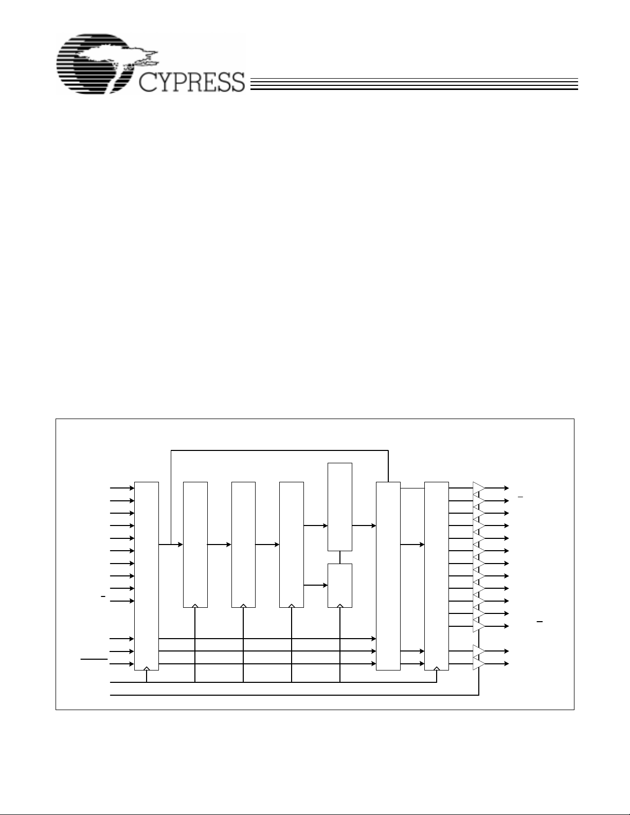
Logic Block Diagram
The inputs of t he CY7C9335 are desi gned to be di rectly mat ed
to a CY7B9334 HOTLink receiver, which converts the
SMPTE-259M compatible high-speed serial data stream into
10-bit parallel characters .
This device performs both TRS (sync) detection and framing,
data descrambling with the SMPTE-259M X
9
+ X4 + 1 algorithm, and NRZI- to-NRZ de coding. The se func tions oper ate a t
any character rate from 16 to 40 MHz. For those systems operating with non- SMPTE-259M compliant vi deo streams (or f or
diagnostic purposes), the descrambler and NRZI decoding
functions can be disabled.
DVB-ASI Operation
The CY7C9335 also contains the necessary mul tiplex ers, control inputs and outputs, to control a DVB-ASI compliant video
stream. DVB-ASI operation is enabled through activat ion of a
single input signal. This allows a single serial-to-parallel input
port to support both SMPTE a nd D VB d ata stre ams under software or hardware control.
In DVB-ASI mode the CY7C9335 automatically enables both
the 8B/10B decoder and multi-byte framer present in the
CY7B9334 receiver/deserializer. All error detection, fill, and
command codes are detected and output by the CY7C933 5.
The CY7C9335 oper ates from a sing le +5V o r −5V supply. It is
available in a 100-pin TQFP space saving package.
D9(RVS)
D
8
D
7
D
6
D
5
D
4
D
3
D
2
D
1
D0(SC/D)
11
10
NRZI-TO-NRZ DECODER
10
SMPTE DESCRAMBLER
TRS DETECTOR/FRAMER
INPUT REGISTER
SYNC_EN
BYPASS
DVB_EN
CKR
OE
HOTLink is a trademark of Cypress Semiconductor Corporation.
Cypress Semiconductor Corporation
• 3901 North First Street • San Jose • CA 95134 • 408-943-2600
19
4
10
BARREL SHIFTER
10
OFFSET
MODE MULTIPLEXOR
RF
A/B
(SVS)
PD
9
PD
8
PD
7
PD
6
PD
5
PD
4
PD
3
PD
2
OUTPUT REGISTER
PD
1
PD0(SC/D)
H_SYNC
SYNC_ERR
March 19
1999
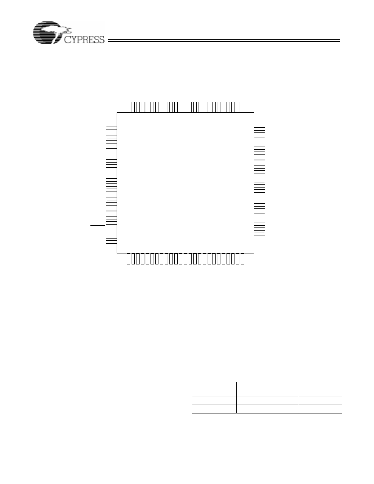
Pin Configuration
CY7C9335
TQFP
Top Vi ew
V
SS
V
SS
NC
NC
NC
NC
NC
NC
NC
OE
V
SS
V
CC
NC
V
SS
V
SS
BYPASS
NC
NC
SYNC_EN
NC
NC
DVB_EN
NC
V
CC
NC
(RVS)
28
NC
29
(RVS)
PD
9
D
D8D7D6D5VCCVSSV
33
32
31
30
NC
NC
PD8PD7PD6PD
9
34
35
5
NC
VCCA/BRFNC
9998979695949392919089888786858483828180797877
100
1
2
3
4
5
6
7
8
9
10
11
12
13
14
15
16
17
18
19
20
21
22
23
24
25
27
26
SS
NC
V
36
V
CC
SS
SS
V
42
41
40
39
38
37
3
SS
SS
CC
CC
NC
V
V
V
PD4PD
D1D2D3D4V
44
43
NC
PD2PD
(SC/D)
0
NC
D
46
45
1
NC
NC
47
NC
SS
V
NC
49
48
CC
V
(SC/D)
0
PD
NC
76
50
NC
75
74
73
72
71
70
69
68
67
66
65
64
63
62
61
60
59
58
57
56
55
54
53
52
51
V
SS
V
CC
NC
NC
NC
NC
NC
NC
NC
NC
CKR
V
SS
NC
V
CC
V
SS
NC
NC
SYNC_ERR
NC
H_SYNC
NC
NC
NC
V
SS
NC
Maximum Ratings
(Abov e which the useful life may be impaired. For user guidelines, not tested.)
Storage Temperature .....................................−40°C to +125°C
Supply Voltage to Ground Potential..................−0.5V to +7.0V
DC V oltage Applied to Outputs
in High-Z State.....................................................−0.5V to +7.0V
Output C ur re n t In to Outpu ts ...... .. .......... .......... .. ..........16 mA
DC Input Voltage.................................................−0.5V to +7.0V
Static Discharge Voltage................................................>2001 V
(per MIL-STD-883, Method 3015)
Latch-Up Current............................................................>200 mA
Operating Range
Range
Commercial 0°C to +70°C 5V ± 5%
Industrial
2
Ambient
Temperature V
−40°C to +85°C
5V ± 10%
CC
CY7C9335
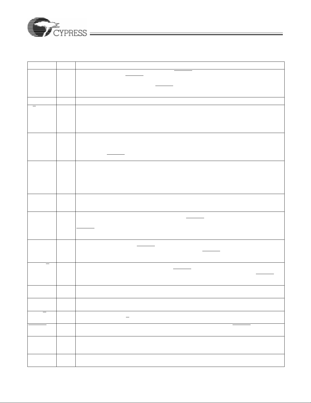
Pin Descriptions
CY7C9335 SMPTE-259M Decoder
Name I/O Description
BYPASS Input Bypass SMPTE decoding. BYPASS is ignored if DVB_EN is acti ve (LOW). If BYPASS is HIGH at the
rising edge of CKR (and DVB_ EN
the NRZI decoder and t he SMPTE d escramb ler and present ed to t he outp ut regi ster. If BYP ASS is LO W
at the risin g edge of t he CKR cloc k (a nd D VB_EN
through the NRZI decod er and SMPTE scrambler.
RF Output Reframe. Thi s output is the inverted DVB-EN signal .
A/B Output CY7B9334 Port Select. When in DVB-ASI mode , this output will alt ernately select either the INA± or INB±
receiver port based on errors dete cted in the dat a stream. This al lows CY7C9335 to ope rate wit h normal
and inverted DVB-ASI data streams ( as would be commonly found on DVB-ASI streams routed through
SMPTE switches). This requires the CY7B9334 INA± and INB± inputs to be connect ed to the same
signal, b ut wi th INB± connected to invert the signal.
H_SYNC Output Horizontal Sync. This out put toggles once e very time that the TRS field is recognized. It changes state
one clock cycle prior to the first character of the TRS field (3FF in 10-bit hex) appearing at the PD
outputs. This output also tog gles to indicate de tection of a TRS sequ ence, ev en when the TRS charact ers
are at a different offset from the present offset and SYNC_EN is active (HIGH). This toggling action is
disabled when DVB_EN
is active (LOW).
SYNC_EN Input Sync Filtering Enab led. Thi s input cont rols the op eration of t he SMPTE framer . When t his signal is activ e
(HIGH) and a TRS se quenc e is d etecte d, if the 10- bit char acter boundary i s di ff er ent f rom the pr e viousl y
received TRS, the H_SYNC output is toggled, b ut the cha ra cter offs et is not updated. If the i mmediatel y
foll owing TRS also has a different offset, the H_SYNC output is agai n toggled and the character offset
is updated to match that of the detected TRS sequence . When this signal is inactive (LOW), the framer
will update the char acter offset and toggle H_SYNC on every detected TRS sequenc e.
SYNC_ERR Output Sync Error. This output pulses HIGH for one CKR clock period when a TRS sequence is detect ed that
is offset fro m its previ ous 10-bit charact er offset. This pul se starts at the same time as the H_SYNC si gnal
toggles, but only occurs when SYNC_EN is active (HIGH) and the character offset is not updated.
PD9(RVS) Output Paralle l Data 9 or Receiv ed Violation Sym bol. This is the MSB of the framed out put data b us. It is la tched
in the output register at the rising edge of CKR. When DVB_EN
that the chara cter present on PD
DVB_EN
is disabled (HIGH), the charac ter in the out put register bits PD
character of the SMPTE data stream.
PD
8−1
Output Paral lel Data 8 through 1. The signals present at the PD
the rising edge of CKR. When DVB_EN
descramb led and framed SMPTE 10-bit data character. When DVB_EN
are full DVB-ASI data bu s.
PD0(SC/D) Output Parallel Data 0 or Special Code/Data Select. This is the LSB of th e output data field. It is la tched in the
output regi ster at the rising edge of CKR. When DVB_EN
character present in PD
inactiv e (HIGH), this output data bit is the LSB of the descrambled and framed SMPTE data cha racter .
8−1
D9(RVS) Input Input Bit 9. This is the MSB of the input register . It should be connected directly to the CY7B9334
deserializer output signal RVS(Q
D
8−1
Input Input Bits 8 through 1. These signal s sho uld be connect ed direc tly to the CY7B9334 deserial izer outp ut
signals Q
respectively.
7−0
D0(SC/D) Input Input Bit 0. This is the LSB of the input register. It should be connected directly to the CY7B9334 dese-
rializer output signal SC/D
DVB_EN Input D VB Mode Enabl e. This signal is sampled b y the rising edge of the CKR cl ock. If D VB_EN is act ive ( LOW ),
the data present on the D
CKR Input Recov ered Cloc k Read. This clock control s all sync hronous oper a tions of the CY7C9335 . It oper ates at
the character rate which is equivalent to one tenth the deseri alized bit-rate. This clock is driven directly
by the CKR output of the CY7B9334 deserializer.
OE Input Output Enable. When this signal is HIGH all outputs are driven to their normal logic le vels. When LOW,
all outputs are placed in a High-Z state.
is HIGH), t he data lat ched into the i nput r egist er is r outed around b oth
is HIGH), the data present i n the inp ut regis ter is routed
is active (LOW), this output indicates
identifies the type of error detected in the character stream. When
8−0
outputs are l atched in the output register at
8−1
is a descrambl ed and framed
9−0
is disabled (HIGH), these signal s are the middle eight bits of the
is active (LOW), these signals
is activ e (LOW), thi s output identi fi es that the
is either a command (HIGH) or data (LOW ) character). When DVB_EN is
).
j
(Qa).
inputs are latched and routed to the PD
0−9
outputs.
0−9
0−9
3
 Loading...