

Datasheet CY7C4841-25AC, CY7C4841-15AC, CY7C4841-10AC, CY7C4831-25AC, CY7C4831-15AC Datasheet (Cypress Semiconductor)
...
256/512/1K/2K/4K/8K x9 x2
Double S
y
nc FIFOs
fax id: 5414
CY7C4801/4811/4821
CY7C4831/4841/4851
Cypress Semiconductor Corporation • 3901North First Street • San Jose • CA 95134 • 408-943- 2600
October 1996 - Revised January 15, 1997
1Double CY7C483 1/4
841/4851
Features
• Double high speed, low power, first-in first-out (FIFO)
memories
• Double 256 x 9 (CY7C4801)
• Double 512 x 9 (CY7C4811)
• Double 1K x 9 (CY7C4821)
• Double 2K x 9 (CY7C4831)
• Double 4K x 9 (CY7C4841)
• Double 8K x 9 (CY7C4851)
• Functionally equivalent to two CY7C4201/4211/4221/
4231/4241/4251 FIFOs in a single package
• 0.65 micron CMOS for optimum speed/power
• High-speed 100-MHz operation (10 ns read/write cycle
times)
• Offers optimal combination of large capacity, high
speed, design flexibility, and small footprint
• Fully asynchronous and simultaneous read and write
operation
• Four status flags per device: Empty, Full, and programmable Almost Empty/Almost Full
• Low power — I
CC1
= 60mA
• Output Enable (OEA
/OEB) pins
• Depth Expansion Capabilty
• Width Expansion Capabilty
• Space-saving 64-pin TQFP
• Pin compatible and functionally equivalent to IDT72801,
72811, 72821, 72831, 72841,72851
Functional Description
The CY7C48X1 are Double high-speed, low-power, first-in
first-out (FIFO) memories with clocked read a nd write in terfaces. All are 9 bits wide and operate as two separate FIFOs. The
CY7C48X1 are pin-compatible to IDT728X1. Programmable
features include Almost Full/Almost Empty flags. These FIF Os
provide solutions for a wide variety of data buffering needs,
including high-speed data acquisition, multiprocessor interfaces, and communications buffering.
These FIFOs have two independent sets of 9-bit input and
output ports that are controlled by separate clock and enable
signals. The input port is contr olled by a free-running clock
(WCLKA,WCLKB) and two write-enable pins (WENA1
,
WENA2/LDA
, WENB1, WENB2/LDB).
When (WENA1
,WENB1) is LOW and (WENA2/LDA,
WENB2/LDB
) is HIGH, data is writ ten into the FIFO on the
rising edge of the (WCLKA,WCLKB) signal. While (WENA1
,
WENA2/LDA
, WENB1, WENB2/LDB) is held active, data is
continually written into the FIFO on each WCLKA, WCLKB
cycle. The output port is controlled in a similar manner by a
free-running read clock (RCLKA, RCLKB) and two read-enable pins ((RENA1
,RENB1), (RENA2,RENB2)). In addition,
the CY7C48X1 has output enable pins (OEA
, OEB) for each
FIFO. The read (RCLKA, RCLKB) and write (WCLKA,
WCLKB) clocks may be tied together for single-clock o peration
or the two clocks may be run independently for asynchronous
read/write appli cations. Clock frequencies up to 100 MHz are
achievable.
Depth expansion is possible using one e nable input for system
control, while the other enable is controlled by expan sion logic
to direct the flow of data.
The CY7C48X1 provides two sets of four different status pins: Empty,
Full, Almost Empty, Almost Full. The Almost Empty/Almost Full flags
are programmable to single word granularity. The programmable
flags default to Empty+7 and Full–7.
The flags are synchronous, i.e., th ey change state relative to
either the read clock (RCLKA,RCLKB) or the write clock
(WCLKA,WCLKB). When entering or exiting the Empt y and
Almost Empty states, the flags are updated exclusively by the
(RCLKA,RCLKB). The flags denoting Almost Full, and Full
states are updated exclusively by (WCLKA,WCLKB) The synchronous flag architecture guarantees that the flags maintain
their status for at least one cycle
All configurations are fabricated using an advanced 0.65µ
N-Well CMOS technology. Input ESD protection is greater than
2001V , and latch-up is prevented by the use of guard rings.
CY7C4801/4811/4821
CY7C4831/4841/4851
2
Logic
Block Diagram
48X1–1
THREE–STATE
OUTPUT
REGISTER
READ
CONTROL B
FLAG
LOGIC
WRITE
CONTROL
WRITE
POINTER B
READ
POINT ER B
RESET
LOGIC
FLAG
PROGRAM
REGISTER
DB
0-8
RCLKB
EFA
PAEA
PAFA
QB
0-8
RSA
OEB
RAM
ARRAY A
256
x9
.
.
8k x
9
RENB1
RENB2
FFA
WRITE
CONTROL
WRITE
POINTER A
WENA1
WCLKA
WENA2/LDA
RSB
WENB1
WCLKB
WENB2/LDB
RAM
ARRAY B
.
.
8k x 9
READ
CONTROL A
READ
POINTER A
RCLKA
RENA1
RENA2
INPUT
REGISTER
DA
0-8
QA
0-8
LDA
LDB
EFB
PAEB
PAFB
FFB
OEA
INPUT
REGISTER
THREE–STATE
OUTPUT REGISTER
256
x9
TQFP
Top View
48X1–1
QA
2
QA
3
QA
4
QA
5
QA
6
QA
7
QA
8
V
cc
WENA2/LDA
WCLKA
WENA1
RSA
DA
8
DA
7
DA
6
QA
1
QB
0
FFB
EFB
OEB
RENB2
RCLKB
RENB1
GND
V
cc
PAEB
PAFB
DB
0
DB
1
DB
2
DB
3
DB
4
48
47
46
45
44
43
42
41
40
39
38
37
36
35
34
33
1
2
3
4
5
6
7
8
9
10
11
12
13
14
15
16
CY7C4801
CY7C4811
CY7C4821
CY7C4831
CY7C4841
CY7C4851
Pin Configuratio n
CY7C4801/4811/4821
CY7C4831/4841/4851
3
Maximum Ratings
(Above which the useful life may be impaired. For user guidelines, not tested.)
Storage Temperature .......................................−65
°C to +150°C
Ambient Temperature with
Power Applied.................................................... −55
°C to +125°C
Supply Voltage to Ground Potential.... .............−0.5V to +7.0V
DC Voltage Applied to Outputs
in High Z State.....................................................−0.5V to +7.0V
DC Input Voltage.................................................−0.5V to +7.0V
Output Current into Outputs (LOW).............................20 mA
Static Discharge Voltage ...........................................>2001V
(per MIL-STD-883, Method 3015)
Latch-Up Current .....................................................>200 mA
Selectio n Guide
7C48X1-10 7C48X1-15 7C48X1-25 7C48X1-35
Maximum Frequency (MHz) 100 66.7 40 28.6
Maximum Access Time (ns) 8 10 15 20
Minimum Cycle Time (ns) 10 15 25 35
Minimum Data or Enable Set-Up (ns) 3 4 6 7
Minimum Data or Enable Hold (ns) 0.5 1 1 2
Maximum Flag Delay (ns) 8 10 15 20
Active Power Supply
Current (I
CC1
) (mA)
Commercial 60 60 60 60
Industrial 70 70 70 70
CY7C4801 CY7C4811 CY7C4821 CY7C4831 CY7C4841 CY7C4851
Density Double 256 x 9 Double 512 x 9 Double 1K x 9 Double 2K x 9 Double 4K x 9 Double 8K x 9
Package 64-pin TQFP 64-pin TQFP 64-pin TQFP 64-pin TQFP 64-pin TQFP 64-pin TQFP
Operating Range
Range
Ambient
Temperatur e
V
CC
Commercial 0°C to +70 °C 5V ± 10%
Industrial
[1]
−40°C to +85°C 5V ± 10%
Notes:
1. T
A
is the “instant on” c ase tempe rature.
CY7C4801/4811/4821
CY7C4831/4841/4851
4
Pin Definitions
Signal Name Description I/O Description
DA
0 − 8
Data Inputs I Data Inputs for 9-bit bus
DB
0 − 8
Data Inputs I Data Inputs for 9-bit bus
QA
0 − 8
Data Outputs O Data Outputs for 9-bit bus
QB
0 − 8
Data Outputs O Data Outputs for 9-bit bus
WENA1
WENB1
Write Enable 1 I WENA1 and WENB1become the only write enables when the device is configured to
have programmable flags. Data is written on a LOW-to-HIGH transition of WCLK when
(WENA1
,WENB1) is LOW and (FFA,FFB) is HIGH. If the FIFO is configured to have two write
enables, data is written on a LOW-to-HIGH transition of WCLK when (WENA1
,WENB1) i s
LO W a n d ( WENA2 /LD A
,WENB2/LDB ) and (FFA,FFB) are HIGH.
WENA2/LDA
WENB2/LDB
Dual Mode Pin
Write Enable 2 I If HIGH at reset, this pin operates as a second write enable. If LOW at reset, this pin
operates as a control to write or read the programmable flag offsets. (WENA1
,WENB1)
mu s t b e LOW and (WENA2/LDA
,WENB2/LDB ) must be HIGH to write data into the FIFO.
Data will not be written into the FIFO if the (FFA
,FFB) is LOW. If the FIFO is configured to have
programmable flags, (WENA2/LDA
,WENB2/LDB) is held LOW to write or read the program-
mable flag offsets.
Load I
RENA1
RENA2
RENB1
RENB2
Read Enable
Inputs
I Enables the device for Read operation.
WCLKA
WCKLB
Write Clock I The rising edge clocks data into the FIFO when (WENA1,WENB1) is LOW and
(WENA2/LDA
,WENB2/LDB) is HIGH and the FIFO is not Full. When
(WENA2/LDA
,WENB2/LDB) is asserted, WCLK writes data into the programmable flag-offset
register.
RCLKA
RCLKB
Read Clock I The rising edge clock s data out of the FIFO when (RE NA 1 ,RENB1) and (RENA2,RENB2)
are LOW and the FIFO is not Empty. When (WENA2/LDA,
WENB2/LDB) is LOW,
(RCLKA,RCLKB) reads data out of the programmable flag-offset register.
EFA,EFB Empty Flag O When (EFA,EFB) is LOW, the FIFO is empty. (EFA,EFB) is synchronized to (RCLKA,RCLKB).
FFA,FFB Full Flag O When (FFA,FFB) is LOW, t h e FIFO is full. ( FF A,FFB) is synchronized to (WCLKA,WCLKB).
P AEA
P AEB
Programmable
Almost Empty
O When (PAEA,PAEB) is LOW , the FIFO is almost empty based on the almost empty offset value
programmed into the FIFO. PAE is synchronized to RCLK.
PAFA
PAFB
Programmable
Almost Full
O When (PAFA,PAFB) is LOW, the FIFO is almost full based on the almost full offset value pro-
grammed into the FIFO. PAF is synchronized to WCLK.
RSA
RSB
Reset I Resets device to empty condition. A reset is required before an initial read or write
operation after power-up.
OEA
OEB
Output Enable I When (OEA,OEB) is LOW , the FIFO’s data outputs drive the bus to which they are connected.
If (OEA
,OEB) is HIGH, the FIFO’s outputs are in High Z (high-impedance) state.

CY7C4801/4811/4821
CY7C4831/4841/4851
5
Electrical Characteristics Over the Operating Range
[2]
7C48X1-10 7C48X1-15 7C48X1-25 7C48X1-35
Parameter Description Test Conditions Min. Max. Min. Max. Min. Max. Min. Max. Unit
V
OH
Output HIGH Voltage VCC = Min.,
I
OH
= −2.0 mA
2.4 2.4 2.4 2.4 V
V
OL
Output LOW Voltage VCC = Min.,
I
OL
= 8.0 mA
0.4 0.4 0.4 0.4 V
V
IH
Input HIGH Voltage 2.0 V
CC
2.0 V
CC
2.0 V
CC
2.0 V
CC
V
V
IL
Input LOW Voltage −0.5 0.8 −0.5 0.8 −0.5 0.8 −0.5 0.8 V
I
IX
Input Leakage
Current
V
CC
= Max. −10 +10 −10 +10 −10 +10 −10 +10 µA
I
OS
[3]
Output Short
Circuit Current
VCC = Max.,
V
OUT
= GND
−90 −90 −90 −90 mA
I
OZL
I
OZH
Output OFF,
High Z Current
OE > VIH,
V
SS
< VO < V
CC
−10 +10 −10 +10 −10 +10 −10 +10 µA
I
CC1
[4]
Active Power Supply
Current
Com’l 60 60 60 60 mA
Ind 70 70 70 70 mA
Capacitance
[5]
Par amete r Description Test Conditions Max. Unit
C
IN
Input Capacitance TA = 25°C, f = 1 MHz,
V
CC
= 5.0V
10 pF
C
OUT
Output Capacitance 10 pF
AC Test Loads and Waveforms
[6, 7]
Notes:
2. See the last page of this specification for Group A subgroup testing information.
3. Test no more than one output at a time for not more than one second.
4. Outputs open. Tested at Frequency = 20 MHz.
5. Tested initially and after any design or process changes that may affect these parameters.
6. C
L
= 30 pF for all AC par amet ers except for t
OHZ
.
7. CL = 5 pF for t
OHZ
.
3.0V
5V
OUTPUT
R1 1.1K
Ω
R2
680Ω
C
L
INCLUDING
JIGAND
SCOPE
GND
90%
10%
90%
10%
≤ 3ns ≤ 3
ns
OUTPUT 1.91V
Equivalentto: THÉ VENIN EQUIVALENT
48X1–4
420Ω
ALL INPUT PULSES
48X1–5
CY7C4801/4811/4821
CY7C4831/4841/4851
6
Switching Characteristics Over the Operating Range
7C48X1-10 7C48X1-15 7C48X1-25 7C48X1-35
Parameter Description Min. Max. Min. Max. Min. Max. Min. Max. Uni t
f
S
Clock Cycle Frequency 100 66.7 40 28.6 MHz
t
A
Data Access Time 2 8 2 10 2 15 2 20 ns
t
CLK
Clock Cycle Time 10 15 25 35 ns
t
CLKH
Clock HIGH Time 4.5 6 10 14 ns
t
CLKL
Clock LOW Time 4.5 6 10 14 ns
t
DS
Data Set-Up Time 3.5 4 6 7 ns
t
DH
Data Hold Time 0.5 1 1 2 ns
t
ENS
Enable Set-Up Time 3.5 4 6 7 ns
t
ENH
Enable Hold Time 0. 5 1 1 2 ns
t
RS
Reset Pulse Width
[8.]
10 15 25 35 ns
t
RSS
Reset Set-Up Time 8 10 15 20 ns
t
RSR
Reset Recovery Time 8 10 15 20 ns
t
RSF
Reset to Flag and Output Time 10 15 25 35 ns
t
OLZ
Output Enable to Output in Low Z
[9]
0 0 0 0 ns
t
OE
Output Enable to Output Valid 3 7 3 8 3 12 3 15 ns
t
OHZ
Output Enable to Output in High Z
[9]
3 7 3 8 3 12 3 15 ns
t
WFF
Write Clock to Full Flag 8 10 15 20 ns
t
REF
Read Clock to Empty Flag 8 10 15 20 ns
t
PAF
Clock to Programmable Almost-Full Flag 8 10 15 20 ns
t
PAE
Clock to Programmable Almost-Full Flag 8 10 15 20 ns
t
SKEW1
Skew Time between Read Clock and Write
Clock for Empty Flag and Full Flag
5 6 10 12 ns
t
SKEW2
Skew Time between Read Clock and Write
Clock for Almost-Empty Flag and Almost-Full
Flag
15 15 18 20 ns
Notes:
8. Pulse widths less than minimum values are not allowed.
9. Va lues guaranteed by design, not currently tested.
CY7C4801/4811/4821
CY7C4831/4841/4851
7
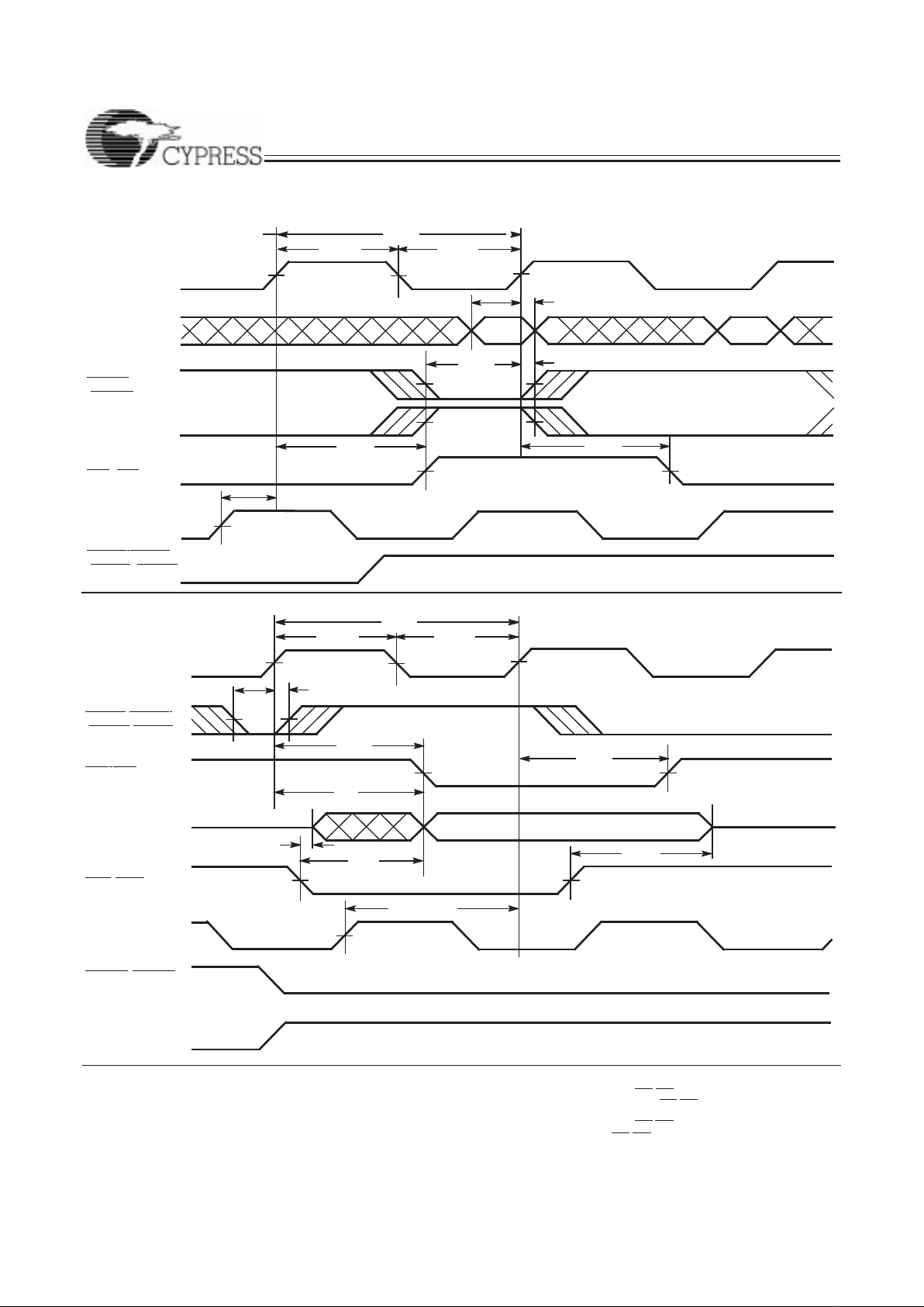
Switching Waveforms
Notes:
10. t
SKEW1
is the minimum time between a r ising (RCLKA,RC LKB) edge and a r ising (WCLKA, WCLKB) edge to guarantee that (FF A,FFB) will go HIGH during the current clock
cycle. If the time between the rising e dge of (R CLKA,RC LKB) an d the rising edg e of ( WCLKA,WCL KB) i s les s than t
SKEW1
, then (FF A,F FB) may not change sta te unt il the
next (WCLKA,WCLKB) rising edge .
11. t
SKEW1
is the minimum time between a rising ( WCLKA,WCLKB) edge and a risi ng (RCLKA,RCLKB) edge to guarantee that (EF A,EFB) will go HIGH during the current clock
cycle. It the time between the rising e dge of (WCLKA, WCLKB) a nd the rising edg e of R CLK is l ess than t
SKEW1
, then (EF A,EFB) may not change s tat e until t he next
(RCLKA,RCLKB) rising edge.
Write Cycle Timing
t
CLKH
t
CLKL
NO OPERATION
t
DS
t
SKEW1
t
ENS
WENA1
t
CLK
t
DH
t
WFF
t
WFF
t
ENH
WCLKA (WCLKB)
DA
0
−DA
8
FFA (FFB)
RENA1
,RENB2
RCLKA (RCLKB)
48X1–6
NO OPERATION
WENA2(WENB2)
(if applicable )
(WENB1
)
(RENB1
, RENB2)
(DB
0
−DB8)
[10]
Read Cycle Timing
t
CLKH
t
CLKL
NO OPERATION
t
SKEW1
t
CLK
t
OHZ
t
REF
t
REF
t
OE
t
ENS
t
OLZ
t
A
t
ENH
VALID DATA
48X1–7
EFA(EFB)
WCLKA,WCLKB
OEA
(OEB)
WENA2(WENB2)
QA
0
−QA
8
(QB0−QB8)
[11]
(RENB1,RENB2)
RENA1
,RENA2
WENA1(WENB1)
RCLKA (RCLKB)

CY7C4801/4811/4821
CY7C4831/4841/4851
8
Notes:
12. The clocks (RCLKA,RCLKB, WCLKA,WCLKB) can be free-running during reset.
13. After reset, the outputs will be LOW if (OEA
,OEB) = 0 and three-state i f (OEA,OE B)=1.
14. Holding (WEN A2/LDA ,WENB2/LDB) HIGH during reset will make the pin act as a second enable pin. Holding(WENA2/LDA,WENB2/LDB) LOW during r eset will make the
pin act as a load enable for the p rogrammab le fl ag of fset registe rs.
Switching Waveforms (continued)
Reset Timing
t
RS
t
RSR
QA0−QA
8
RSA(RSB)
t
RSF
t
RSF
t
RSF
OEA(OEB)=1
OEA
(OEB)=0
RENA1
, RENA2
(RENB1,RENB2)
EFA, PAEA
FFA, PAFA
48X1–8
t
RSS
t
RSR
t
RSS
t
RSR
t
RSS
WENA2/LDA
WENA1
(WENB1)
(WENB2/LDB
)
(EFB
, PAEB)
(FFB, PAFB)
(QB0−QB8)
[12]
[13]
[14]

CY7C4801/4811/4821
CY7C4831/4841/4851
9
Notes:
15. When t
SKEW1
> minimum specification, t
FRL
(maximum) = t
CLK
+ t
SKEW1
. When t
SKEW1
< minimum specific ation, t
FRL
(maximum) = either 2*t
CLK
+ t
SKEW1
or t
CLK
+ t
SKEW1
.
The Latency T im ing appli es only at the Empt y Boundar y (EFA, EFB= LOW).
16. The first word is available the cycle after (EFA, EFB) goes HIGH, always.
Switching Waveforms (continued)
(RENB1,RENB2)
D
0
(FIRSTVALIDWRITE)
First Data Word Latency after Reset with Simultaneous Read and Writ e
t
SKEW1
WENA1(WENB1)
WCLKA,WCLKB
QA
0
−QA
8
EFA(EFB)
RENA1
, RENA2
OEA(OEB)
t
OE
t
ENS
t
OLZ
t
DS
RCLKA(RCLKB)
t
REF
t
A
t
FRL
D
1
D
2
D
3
D
4
D
0
D
1
DA0−DA
8
48X1–9
t
A
WENA2(WENB2)
(if applicable )
(DB
0
−DB8)
(QB
0
−QB8)
[15]
[16]

CY7C4801/4811/4821
CY7C4831/4841/4851
10
Switching Waveforms (continued)
WENA2(WE NB2)
(if applicable )
DATA WRITE2
DATA WRITE1
t
ENS
t
SKEW1
DATA IN OUTPUT REGISTER
Empty Flag Timing
WENA1(WE NB1)
WCLKA,WCL KB
QA
0
−QA
8
EFA(EFB)
RENA1
, RENA2
(RENB1,RENB2)
OEA(OEB)
t
DS
t
ENH
RCLKA(RCLKB)
t
REF
t
A
t
FRL
DA0−DA
8
DATA READ
t
SKEW1
t
FRL
t
REF
t
DS
t
ENS
t
ENH
48X1–10
t
ENS
t
ENH
t
ENS
t
ENH
t
REF
LOW
(DB
0
−DB8)
(QB
0
−QB8)
[15]
[15]

CY7C4801/4811/4821
CY7C4831/4841/4851
11
Switching Waveforms (continued)
Full Flag Timing
QA0−QA
8
RENA1, RENA2
(RENB1,RENB2)
WENA1(WENB1)
WENA2(WENB2)
(if applicable )
DA
0
−DA
8
NEXT DATA READ
DATA WRITE
NO WRITE
DATA IN OUTPUT REGISTER
FFA(FFB)
WCLKA,WCLKB
OEA(OEB)
RCLKA(RCLKB)
t
A
DATA READ
t
SKEW1
t
DS
t
ENS
t
ENH
t
WFF
t
A
t
SKEW1
t
ENS
t
ENH
t
WFF
DATA WRITE
NO WRITE
t
WFF
LOW
48X1–11
NO WRITE
(DB
0
−DB8)
(QB
0
−QB8)
[10]
[10]

CY7C4801/4811/4821
CY7C4831/4841/4851
12
Notes:
17. t
SKEW2
is the minimum time betwe en a ri sing (WC LKA,WCLK B) and a r isi ng (RCLKA,R CLKB) edge for (PAEA,P AEB ) t o change st ate during t hat c lock cycle. I f the time
between the e dge of (WCL KA,WC LKB) a nd the ris ing ( RCLKA, RCLKB) i s less t han t
SKEW2
, then (PAEA,PAEB ) may not change state until the n ext RCL K.
18. (PAEA,PAEB) offset = n.
19. If a read is preformed on this rising edge of the read clock, there will be Empty + (n-1) words in the FIFO when (PAEA,PAEB ) goes LOW.
20. If a write is performed on this rising edge of the write clock, there will be Full - (m-1) words of the FIFO when (PAFA,PAFB) goes LOW.
21. (PAFA,PAFB) offset = m.
22. 256-m words in FIFO for CY7C4801, 512-m words for CY7C4811, 1024-m words for CY7C4821, 2048-m words for CY7C4831, 4096-m words for CY7C4841,
8192-m words for CY7C4851.
23. t
SKEW2
is the minimum time betwe en a r ising (RCLKA,RC LKB ) edge and a r ising (WCLKA,WC LKB) ed ge for (PAFA,PAFB) to change during that clock cycle. If the time
between the ris ing edge of (RCL KA,RCLKB) and t he rising edge of (WCLK A,WCLKB) is less tha n t
SKEW2
, then (PA F A,PAFB) may not change s tate until th e nex t
(WCLKA,WCLKB).
Switching Waveforms (continued)
t
ENH
ProgrammableAlmost Empty Flag Timing
t
CLKH
t
ENS
t
CLKL
t
PAE
N +1 WORDS
IN FIFO
48X1–12
t
ENH
t
ENS
t
ENH
t
ENS
t
PAE
t
SKEW2
[17]
WCLKA,WCLKB
PAEA
(PAEB)
RCLKA(RCLKB)
RENA1
, RENA2
(RENB1,RENB2)
WENA1(WENB1)
WENA2(WENB2)
(if applicable )
Note
18
Note
19
t
ENH
Programmable Almost Full Flag Timing
t
CLKH
t
ENS
FULL− M WORDS
IN FIFO
t
CLKL
t
ENS
FULL− M+1 WORDS
IN FIFO
48X1–13
t
ENH
t
ENS
t
ENH
t
ENS
t
PAF
t
SKEW2
t
PAF
[22]
[23]
WCLKA,WCLKB
PAFA
(PAFB)
RCLKA(RCLKB)
RENA1
, RENA2
(RENB1,RENB2)
WENA1(WENB1)
WENA2(WENB2)
(if applicable )
Note
20
Note
21

CY7C4801/4811/4821
CY7C4831/4841/4851
13
Switching Waveforms (continued)
t
ENH
Write Programmable Registers
WENA2/LDA
t
CLKH
t
ENS
t
CLKL
PAE OFFSET
LSB
t
ENS
PAF OFFSET
MSB
t
CLK
t
DS
t
DH
48X1–14
PAE OFFSET
MSB
PAF OFFSET
LSB
WCLKA,WCLKB
DA
0
−DA
8
WENA1(WENB1)
(WENB2/LDB
)
(DB
0
−DB8)
PAF OFFSET
MSB
PAF OFFSET
LSB
t
ENH
Read Programmable Registers
t
CLKH
t
ENS
t
CLKL
PAE OFFSET LSB
t
ENS
PAE OFFSET MSB
t
CLK
UNKNOWN
t
A
48X1–15
WENA2/LDA
RCLKA(RCLKB)
QA
0
−QA
8
RENA1, RENA2
(RENB1,RENB2)
(WENB2/LDB)
(QB
0
−QB8)

CY7C4801/4811/4821
CY7C4831/4841/4851
14
Architectur e
The CY7C48X1 functions as two independent FIFOs in a single
package, each with its own separate set of controls. The device consists of two arrays of 256 to 8K words of 9 bits each (implemented by a dual-port array of SRAM cells), two read pointers,
two write pointers, control signals (RCLKA, RCLKB, WCLKA,
WCLKB, RENA1
, RENB1, RENA2, RENB2, WENA1, WENB1,
WENA2, WENB2, RSA
, RSB), and flags (EFA,EFB, PAE A, PAEB,
PAFA
,PAFB, FF A,FFB).
Resetting the FIFO
Upon power-up, the FIFO must b e reset with a Reset (RSA,
RSB
) cycle. This causes the FIFO to enter the Empty condition sig-
nified by (EFA
,EFB) being LOW. All data outputs (QA
0−8,QB0−8
) go
LOW t
RSF
after the rising edge of RSA, RSB. In order for the FIFO
to reset to its default state, a falling edge must occur on (RSA
,RSB)
and the user must not read or wri te while (RSA
,RSB ) is LOW. All flags
are guaranteed to be valid t
RSF
after (RSA,RSB) is taken LOW.
FIFO Operation
When the (WENA1,WENB1) signal is active LOW and
(WENA2,WENB2) is active HIGH, data present on the
(DA
0−8,DB0−8
) pins is written into the F IFO on each rising edge
(WCLKA,WCLKB) of the ( WCL KA,W CLK B) si gnal. Similarly, when
the (RENA1
,RENB1) and (RENA2,RENB2) signals are active LOW,
data in the FIFO memory will be presented on the (QA
0−8,QB0−8
)
outputs. New data will be presented on each rising edge of
(RCLKA,RCLKB) while (RENA1
,RE NB 1) and (RENA2,RENB2) are
active. ( RENA1
,REN B1) and (RENA2,RENB2) must set up t
ENS
before (RCLKA,RCLKB) for it to be a valid read function.
(WENA1
,WENB1) and (WE NA2,W ENB2) must occur t
ENS
before
(WCLKA,WCLKB) for it to be a valid write function.
An output enable (OEA
,OEB) pin is provided to three-state the
(QA
0− 8,QB0−8
) outputs when (OEA,OEB) is asserted. When
(OEA
,OEB) is enabled (LOW), data in the output register will be avail-
able to the (QA
0−8,QB0−8
) outputs after tO E.
The FIFO contains overflow circuitry to disallow additional
writes when the FIFO is full, and underflow circuitry to disallow
additional reads when the FIFO is empty. An empty FIFO
maintains the data of the last valid r ead on its (QA
0−8,QB0−8
)
outputs even after additional reads occur.
Write Enable 1 (WENA1
,WENB1) - If the FIFO is configured
for programmable flags, Write Enable 1 (WENA1
,WENB1) is
the only write enable control pin. In this configuration, when
Write Enable 1 (WENA1
,WENB1) is LOW, data can be loade d
into the input register and RAM array on the LOW-to-HIGH
transition of every write clock (WCLKA,WCLKB). Data is
stored is the RAM array sequentially and independently of any
on-going read operation.
Write Enable 2/Load (WENA2/LDA, WENB2/LDB) - Thi s is a
dual-purpose pin. The FIFO is configured at Reset to have
programmable flags or to have two write enables, which allows
for depth expansion. If Write Enable 2/Load (WENA2/LDA,
WENB2/LDB) is set active HIGH at Reset (RSA,RSB=LOW),
this pin operates as a second write enable pin.
If the FIFO is configured to have two write enables, when W rite
Enable 1 (WENA1
,WENB1) is LOW and Write Enable 2/Load
(WENA2/LDA
, WENB2/LDB) is HIGH, data can be loaded into the
input register and RAM array on the LOW-to-HIGH transition of every
write clock (WCLKA ,WCL KB) . Data i s stor ed in t he R AM arra y sequentially and independently of any on-going read operation.
Progra mming
When (WENA2/LDA, WENB2/LDB) is held LOW during Reset, this
pin is the load (LDA
,LDB) enable for flag offset programming. In this
configuration, (W EN A2/LDA
, WENB2/LDB) can be used to access
the four 8-bit offset registers contained in the CY7C48X1 for writing
or reading data to these registers.
When the device is configured for programmable flags and
both (WENA2/LDA,
WENB2/LDB) and (WENA1,WENB1) are
LOW, the first LOW-to-HIGH tran sition of (WCLKA,WCLKB ) wr it es
data from the data inputs to the empty offset least significant bit (LSB)
register. The second, third, and fourth LOW-to-HIGH transitions of
(WCLKA,WCLKB) store data in the empty offset most significant bit
(MSB) register, full offset LSB register, and full offset MSB regist er,
respectively, when (WENA2/LDA
, WENB2/LDB) and
(WENA1
,WENB1) are LOW. The fifth LOW-to-HIGH t ransition of
(WCLKA,WCLKB) while (WENA2/LDA
, WENB2/LDB) and
(WENA1
,WENB1) are LOW writes data to t he e mpty LS B r egist er
again.
Figure 1
shows the register sizes and default values for the
various device types.
It is no t necess ary to write to all the offset registers at one time.
A subse t o f the of fset registers can be written; then by bringing
the (WENA2/LDA
, WENB2/LDB) input HIGH, the FIFO is returned
to normal read and write operation. The next time (WENA2/LDA,
WENB2/LDB) is brought LOW, a write operation stores data in the
next offset register in sequence.
The contents of the offset registers can be read to the data
outputs when (WENA2/LDA
, WENB2/LDB) is LOW and both
(RENA1
,RENB1) and (RENA2, RENB2) are LOW. LOW-to-HIGH
transitions of (RCLKA,RCLKB) read register contents to the data outputs. Writes and reads should not be preformed simultane ously on
the offset registers.

CY7C4801/4811/4821
CY7C4831/4841/4851
15
Programmable Flag (PAEA
,PAEB, PAFA,PAFB) Operation
Whether the flag offset registers are programmed as described in
T able 1
or the default values are used, the programmable
almost-empty flag (P AEA
,PAEB) and programmable almost-full flag
(PAFA
,PAFB) states are determined by their corresponding offset
registers and the difference between the read and write pointers.
The number formed by the empty offset least significant bit
register and empty offset most significant register is referred
to as
n
and determines the operation of (PAEA,PAEB).
(PAEA
,PAEB) is synchronized to the LOW-to-HIGH transition of
RCLK by one flip-flop and is LOW when the FIFO contains n or fewer
unread words. (PAEA
,PAEB) is set HIGH by the LOW-to-HIGH transition of RCLK when the FIFO contains (n+1) or greater unread
words.
The number formed by the full offset least significant bit register and full offset most significant bit register is referred to as
m
and determines the operation of (P AFA,PAFB). (PAEA,PAEB) is
synchronized to the LOW-to-HIGH transition of (WCLKA,WCLKB) by
one flip-flop and is set LOW when the number of unread words in the
FIFO is greater than or equal to CY7C4801 (256– m), CY7C4811
(512–m), CY7C4821 (1K–m), CY7C4831 (2K–m), CY7C4841
(4K–m), and CY7C4851 (8K–m). (PAFA
,PAFB) is set HIGH by the
LOW-to-HIGH transition of (W CLKA,WCLKB) when the number of
available memory locations is greater than m.
Notes:
24. The same selection sequence applies to reading form the registers. REN1
and REN2 are enabled and a read is performed on the LOW- to-HIGH transition of
RCLK.
Figure 1. Offset Register Location and Default Values.
256 x 9 x 2 512 x 9 x 2
8
0
8
0
8
0
8
0
1K x 9 x 2
2K x 9 x 2 4K x 9 x 2 8K x
9 x 2
(MSB)
0
(MSB)
0
7
1
7
1
8
0
8
0
8
0
8
0
(MSB)
00
(MSB)
00
7
1
7
1
8
0
8
0
8
0
8
0
(MSB)
000
(MSB)
000
7
2
7
2
8
0
8
0
8
0
8
0
Empty Offset (LSB) Reg.
Default Value = 007h
Full Offset(LSB) Reg
Default Value = 007h
(MSB)
0000
(MSB)
0000
7
3
7
3
Empty Offset (LSB) Reg.
Default Value = 007h
Full Offset(LSB) Reg
Default Value = 007h
Empty Offset (LSB) Reg.
Default Value = 007h
Full Offset(LSB) Reg
Default Value = 007h
Empty Offset(LSB) Reg.
Default Value = 007h
Full Offset(LSB) Reg
Default Value =
007h
8
0
8
0
8
0
8
0
Empty Offset (LSB) Reg.
Default Value = 007h
Full Offset(LSB) Reg
Default Value = 007h
(MSB)
00000
(MSB)
00000
7
4
7
4
8
0
8
0
8
0
8
0
7
7
Full Offset(LSB) Reg
Default Value = 007h
Empty Offset (LSB) Reg.
Default Value =
007h
Table 1. Writing the Offset Registers.
LD WEN WCLK
[24]
Selection
0 0 Empty Offset (LSB)
Empty Offset (MSB)
Full Offset (LSB)
Full Offset (MSB)
0 1 No Op eration
1 0 Write Into FIFO
1 1 No Operation

CY7C4801/4811/4821
CY7C4831/4841/4851
16
Flag Operation
The CY7C48X1 devices provide four flag pins to indicate the
condition of the FIFO contents. Empty, Full, (PAEA
,PAEB), and
(PAFA
,P AF B) are synchronous.
Full Flag
The Full Flag (FFA
,FFB) will go LOW when the device is full. Write
operations are inhibited whenever (FFA
,FFB) is LOW regardless of
the state of (WENA1
,WENB1) and (WENA2/LDA,WENB2/LDB).
(FFA
,FFB) is synchronized to (WCLKA,WCLKB), i.e., it is exclusively
updated by each rising edge of (WCLKA,WCLKB).
Empty Flag
The Empty Flag (EFA
,EFB) will go LOW when the device is empty.
Read operations are inhibited whenever (EFA
,EFB) is LOW, regard-
less of the state of (RENA1
,RENB1) and (RENA2,RENB2.
(EFA
,EFB) is synchronized to (RCLKA,RCLKB), i.e., it is exclusively
Full Flag
Table 2. Stat us Flags.
Number of Words in FIFO
FF PAF PAE EFCY7C4801 CY7C4811 CY7C4821
0 0 0 H H L L
1 to n
[25]
1 to n
[25]
1 to n
[25]
H H L H
(n+1) to (256-(m+1)) (n+1) to (512-(m+1)) (n+1) to (1024 −(m+1)) H H H H
(256−m)
[26]
to 255 (512−m)
[26]
to 511 (1024−m)
[26]
to 1023 H L H H
256 512 1024 L L H H
Number of Words in FIFO
FF PAF PAE EFCY7C4831 CY7C4841 CY7C4851
0 0 0 H H L L
1 to n
[25]
1 to n
[25]
1 to n
[25]
H H L H
(n+1) to (2048 −(m+1)) (n+1) to (4096 −(m+1)) (n+1) to (8192 −(m+1)) H H H H
(2048−m)
[26]
to 2047 (4096−m)
[26]
to 4095 (8192−m)
[26]
to 8191 H L H H
2048 4096 8192 L L H H
Notes:
25. n =Empty Offset (n=7 default value).
26. m = Full Offset (m=7 default value).

CY7C4801/4811/4821
CY7C4831/4841/4851
17
Single Device Configu ration
When FIFO A(B) is in a Single Device Configuration, the Read
Enable 2 RENA2
(RENB2) control input can be grounded (see
Figure 2
). in this configuration, the Write Enable2/Load
(WENA2/LDA
,WENB2/LDB) pin is set LOW at Reset so that
the pin operates as a control to load and read the programmable flag offsets.
Figure 2. Block Diagram of 256 x 9, 512 x 9,1024 x 9,2048 x 9,4096 x 9,8192 x 9 Double Sync FIFO
Used in a Single Device Configuration.
EMPTY FLAG (EFA
,EFB)
48X1–16
WRITE CLOCK (WC LKA,WCLKB)
WRITE ENABLE1(WENA1
,WENB1)
WRITEENABLE2/LOAD(WENA2/LDA
,WENB/LDB)
(PAFA
,PAFB)
FULLFLAG (FFA
,FFB)
CY7C4801
DATA IN DA0−DA8(DB0−DB8)
RESET(RSA
,RSB)
READ CLOCK(RCLKA,RCLKB)
READ ENABLE1 (RENA1
,RENB1)
OUTPUT ENABLE(OEA
,OEB)
PROGRAMMABLE(PAEA
,PAEA)
ReadEnable2 (RENA2,RENB2)
CY7C4811
CY7C4821
CY7C4831
CY7C4841
CY7C4851
DATA OUTQA0−QA8(QB0−QB8)
PROGRAMMABLE

CY7C4801/4811/4821
CY7C4831/4841/4851
18
Width Expansion Configuration
Word width may be increased simply by connecting the corresponding input control signals of FIFOs A and B. A composite
flag should be created for each of the end-point status flags
EFA
and EFB, also FFA and FFB. The partial status flags
PAEA
, PAFB, PAFA, PAFB can be detected from any one de-
vice.
Figure 3
demonstrates an 18-bit word width using the two
FIFOs contained in one CY7C4801/4811/4821/4831/4841
/4851. Any word width can be attained by adding additional
CY7C4801/4811/4821/4831/4841/4851s.
When the CY7C4801/4811/4821/4831/4841/4851 is in a
Width Expansion Configuration, the Read Enable 2 (RENA2
and RENB2) control unputs can be grounded (see
Figure 3
).
In this configuration, the Write Enable 2/Load
(WENA2/LDA
,WENB2/LDB) pins are set LOW at Reset so
that the pin operates as a control to load and read the programmable flag offsets.
Figure 3. Bl ock Diagram of two FIFOs contained in one CY7C4801/4811/4821/4831/4841/4851 configured for an 18-bit
width-expansion.
WRITE ENABLE WENA
(RENA2)
48X1–17
FF
EF
WCLKA
WRITE ENABLE2/LOAD
WEN2/LD
FULLFLAG
FFA
9
18
RESET(RSA)
9
RESET
(RSB
)
RCLKB
READ ENABLE
RENB1
OUTPUT ENABLE
OEB
EMPTY FLAG
EFA
9
9
18
ReadEnable2
EFB
FFB
ReadEnable2 (RENB2)
RAM ARRAY A
RAM ARRAY B
256 x 9
512 x 9
1024 x 9
2048 x 9
4096 x 9
8192 x 9
256 x 9
512 x 9
1024 x 9
2048 x 9
4096 x 9
8192 x 9
RCLKA
WCLKB
WRITECLOCK
READCLOCK
RENA1
WENB1
OEA
WENB2/LDB
RESET
9
D0−D
17
Q0−Q
17

CY7C4801/4811/4821
CY7C4831/4841/4851
19
Bidirectional Configuration
The two FIFOs of the CY7C4801/4811/4821/4831/4841/4851
can be used to buffer data flow in two directions. In the example that follows, processor A can write data to processor B via
FIFO A, and, in turn, processor B can write processor A via
FIFO B.
Depth Expansion
CY7C4801/4811/4821/4831/4841/4851can be adapted to appliations that require greater than 256/512/1024/2048/4096/
8192 words. The existence of dual enable p ins on the read and
write ports allow depth expansion. The Write Enable 2/Load
(WENA2, WENB2) pins are us ed a s a second write enables in
a depth expansion configuration, thus the Programmable flags
are set to the default values. Depth expansion is possible by
using one enable input for system control while the other enable input is controlled by expansion logic to direct the flow of
data. a typical application would have the expansion logic alternate data access fro m one de vice to the ne xt in a sequential
manner. The CY7C4801/4811/4821/4831/4841/ 4851 operates in the Depth Expansion configuration when the following
conditions are met:
1. WENA2/LDA
and WENB2/LDB pins are held HIGH during
Reset so that these pins operate as second W rite Enables .
2. External logic is used to control the flow of data.
Figure 4. Block Diagram of Bidirectional Configurati on.
9
CY7C4801
CY7C4811
CY7C4821
CY7C4831
CY7C4841
CY7C4851
RAM ARRAY A
RAM ARRAY B
WENA2
RENA2
RCLKA
WCLKA
WENA1
DA0−DA
8
OEA
RENA1
QA0−QA
8
WENB2
RENB2
RCLKB
WCLKB
WENB1
DB0−DB
8
OEB
RENB1
QB0−QB
8
V
CC
RAM
PROCESSOR A
CLOCK
ADDRESS
CONTROL
DATA
V
CC
9
9
9
9
9
9
PROCESSOR A
CLOCK
ADDRESS
CONTROL
DATA
9
RAM
48X1–18

CY7C4801/4811/4821
CY7C4831/4841/4851
20
Ordering Info rma tio n
Double 256x9 FIFO
Speed
(ns) O rderi n g Code
Package
Name
Package
Type
Operati ng
Range
10 CY7C4801-10AC A65 6 4-Lead Thin Quad Flatpack Commercial
CY7C4801-10AI A65 64-Lead Thin Quad Flatpack Industrial
15 CY7C4801-15AC A65 6 4-Lead Thin Quad Flatpack Commercial
CY7C4801-15AI A65 64-Lead Thin Quad Flatpack Industrial
25 CY7C4801-25AC A65 6 4-Lead Thin Quad Flatpack Commercial
CY7C4801-25AI A65 64-Lead Thin Quad Flatpack Industrial
35 CY7C4801-35AC A65 6 4-Lead Thin Quad Flatpack Commercial
CY7C4801-35AI A65 64-Lead Thin Quad Flatpack Industrial
Double 512x9 FIFO
Speed
(ns) O rderi n g Code
Package
Name
Package
Type
Operati ng
Range
10 CY7C4811-10AC A65 64-Lead Thin Quad Flatpack Commercial
CY7C4811-10AI A65 64-Lead Thin Quad Flatpack Industrial
15 CY7C4811-15AC A65 64-Lead Thin Quad Flatpack Commercial
CY7C4811-15AI A65 64-Lead Thin Quad Flatpack Industrial
25 CY7C4811-25AC A65 64-Lead Thin Quad Flatpack Commercial
CY7C4811-25AI A65 64-Lead Thin Quad Flatpack Industrial
35 CY7C4811-35AC A65 64-Lead Thin Quad Flatpack Commercial
CY7C4811-35AI A65 64-Lead Thin Quad Flatpack Industrial
Double 1Kx9 FIFO
Speed
(ns) O rderi n g Code
Package
Name
Package
Type
Operati ng
Range
10 CY7C4821-10AC A65 6 4-Lead Thin Quad Flatpack Commercial
CY7C4821-10AI A65 64-Lead Thin Quad Flatpack Industrial
15 CY7C4821-15AC A65 6 4-Lead Thin Quad Flatpack Commercial
CY7C4821-15AI A65 64-Lead Thin Quad Flatpack Industrial
25 CY7C4821-25AC A65 6 4-Lead Thin Quad Flatpack Commercial
CY7C4821-25AI A65 64-Lead Thin Quad Flatpack Industrial
35 CY7C4821-35AC A65 6 4-Lead Thin Quad Flatpack Commercial
CY7C4821-35AI A65 64-Lead Thin Quad Flatpack Industrial

CY7C4801/4811/4821
CY7C4831/4841/4851
21
Document #: 38-00538-A
Ordering Info rma tio n (continued)
Double 2Kx9 FIFO
Speed
(ns) O rderi n g Code
Package
Name
Package
Type
Operati ng
Range
10 CY7C4831-10AC A65 6 4-Lead Thin Quad Flatpack Commercial
CY7C4831-10AI A65 64-Lead Thin Quad Flatpack Industrial
15 CY7C4831-15AC A65 6 4-Lead Thin Quad Flatpack Commercial
CY7C4831-15AI A65 64-Lead Thin Quad Flatpack Industrial
25 CY7C4831-25AC A65 6 4-Lead Thin Quad Flatpack Commercial
CY7C4831-25AI A65 64-Lead Thin Quad Flatpack Industrial
35 CY7C4831-35AC A65 6 4-Lead Thin Quad Flatpack Commercial
CY7C4831-35AI A65 64-Lead Thin Quad Flatpack Industrial
Double 4Kx9 FIFO
Speed
(ns) O rderi n g Code
Package
Name
Package
Type
Operati ng
Range
10 CY7C4841-10AC A65 6 4-Lead Thin Quad Flatpack Commercial
CY7C4841-10AI A65 64-Lead Thin Quad Flatpack Industrial
15 CY7C4841-15AC A65 6 4-Lead Thin Quad Flatpack Commercial
CY7C4841-15AI A65 64-Lead Thin Quad Flatpack Industrial
25 CY7C4841-25AC A65 6 4-Lead Thin Quad Flatpack Commercial
CY7C4841-25AI A65 64-Lead Thin Quad Flatpack Industrial
35 CY7C4841-35AC A65 6 4-Lead Thin Quad Flatpack Commercial
CY7C4841-35AI A65 64-Lead Thin Quad Flatpack Industrial
Double 8Kx9 FIFO
Speed
(ns) O rderi n g Code
Package
Name
Package
Type
Operati ng
Range
10 CY7C4851-10AC A65 6 4-Lead Thin Quad Flatpack Commercial
CY7C4851-10AI A65 64-Lead Thin Quad Flatpack Industrial
15 CY7C4851-15AC A65 6 4-Lead Thin Quad Flatpack Commercial
CY7C4851-15AI A65 64-Lead Thin Quad Flatpack Industrial
25 CY7C4851-25AC A65 6 4-Lead Thin Quad Flatpack Commercial
CY7C4851-25AI A65 64-Lead Thin Quad Flatpack Industrial
35 CY7C4851-35AC A65 6 4-Lead Thin Quad Flatpack Commercial
CY7C4851-35AI A65 64-Lead Thin Quad Flatpack Industrial

CY7C4801/4811/4821
CY7C4831/4841/4851
© Cypress Semiconductor Corporation, 1997. The information contained herein is subject to change without notice. Cypress Semiconductor Corporation assumes no responsibility for the use
of any circuitry othe r than circui try embodi ed in a Cypress Semi conductor p roduct. Nor does it convey or imply any li cense under patent or other rights . Cypress Semi conductor does not authori ze
its products for use as critical components in life-support systems where a malfunction or failure may reasonably be expected to result in significant injury to the user. The inclusion of Cypress
Semiconductor products in life-support systems application implies that the manufacturer assumes all risk of such use and in doing so indemnifies Cypress Semiconductor against all charges.
Package Diagrams
64-Lead Thin Plast ic Quad Flat Pack A65
 Loading...