

Datasheet CY7C4425-25ASC, CY7C4425-25ACT, CY7C4425-15ASC, CY7C4425-15ACT, CY7C4425-15AC Datasheet (Cypress Semiconductor)
...
64, 256, 512, 1K, 2K, 4K x 18 Synchronous FIFOs
fax id: 5410
CY7C4425/4205/4215
CY7C4225/4235/4245
Cypress Semiconductor Corporation • 3901North First Street • San Jose • CA 95134 • 408-943- 2600
April 1995 - Revised August 18, 1997
1CY7C42 25
Features
• High-speed, low-power, first-in first-out (FIFO)
memories
• 64 x 18 (CY7C4425)
• 256 x 18 (CY7C4205)
• 512 x 18 (CY7C4215)
• 1K x 18 (CY7C4225)
• 2K x 18 (CY7C4235)
• 4K x 18 (CY7C4245)
• High-speed 100-MHz operation (10 ns read/write cycle
time)
• Low power (I
CC
=45 mA)
• Fully asynchronous and simultaneous read and write
operation
• Empty, Full, Half Full, and Programmable Almost
Empty/Almost Full status flags
• TTL-compatible
• Retransmit function
• Output Enable (OE
) pin
• Independent read and write enable pins
• Center power and ground for reduced noise
• Supports free-running 50% duty cycle clock inputs
• Width Expansion Capability
• Depth Expansion Capability
• Space saving 64-pin 10x10 TQFP, and 14x14 TQFP
• 68-pin PLCC
Functional Description
T
he CY7C42X5 are high-speed, low-power, first-in first-out
(FIFO) memories with clocked read and write interfaces. All
are 18 bits wide and are pin/functionally compatible to
IDT722x5. The CY7C42 X5 c an be c ascaded to increase FIFO
depth. Programmable features include Almost Full/Almost
Empty flags. These FIFOs provide solutions for a wide variety
of data buffering needs, including high-speed data acquisition,
multiprocessor interf a ces, and communi catio ns buffering.
These FIFOs have 18-bit input and output ports that are controlled by separate clock and enable signals. The input port is
controlled by a free-running clock (WCLK) and a write enable
pin (WEN
).
When WEN
is asserted, data is written into the FIFO on the
rising edge of the WCLK signal. While WEN
is held active, data
is continually writt en into t he FIFO on each cycle. The output
port is controlled in a similar manner by a free-running read
clock (RCLK) and a read enable pin (REN
). In addition, the
CY7C42X5 have an output enable pin (OE
). The read and
write clocks may be tied together for single-clock operation or
the two clocks may be run independently for asynchronous
read/write appli cations. Clock frequencies up to 100 MHz are
achievable.
Retransmit and Synchronous Almost Full/Almost Empty flag
features are available on these devices.
Depth expansion is possible using the cascade input (WXI
,
RXI
), cascade output (WXO, RXO), and First Load (FL) pins.
The WXO
and RXO pins are connected to the WXI and RXI
pins of the next device, and the WXO and RXO pins of the last
device should be connected to the WXI
and RXI pins of the
first device. The FL
pin of the first device is tied to VSS and the
FL
pin of all the remaining devices should be tied to VCC.
The CY7C42X5 provides five status pins. These pins are decoded to determine one of five states: Empty, Almost Empty,
Half Full, Almost Full, and Full (see
T able 2
). The Half Full flag
shares the WXO
pin. This flag is valid in the stan dalone and
width-expansion configurations. In the depth expansion, this
pin provides the expansion out ( WXO
) information that is used
to signal the next FIFO when it will be activated.
The Empty and Full flags are synchronous, i.e., they change
state relative to either the read clock (RCLK) or the write clock
(WCLK). When entering or exiting the Empty states, the flag is
updated exclusively by the RCLK. The flag denoting Full states
is updated exclusively by WCLK. The synchronous flag architecture guarantees that the flags will remain valid from one
clock cycle to the next. As mentioned previously, the Almost
Empty/Almost Full flags become synchronous if the
V
CC
/SMODE is tied to VSS. All configurations are fabricated
using an advanced 0.65µ N-Well CMOS technology. Input
ESD protection is greater than 2001V, and latch-up is prevented by the use of guard rings.
CY7C4425/4205/4215
CY7C4225/4235/4245
2
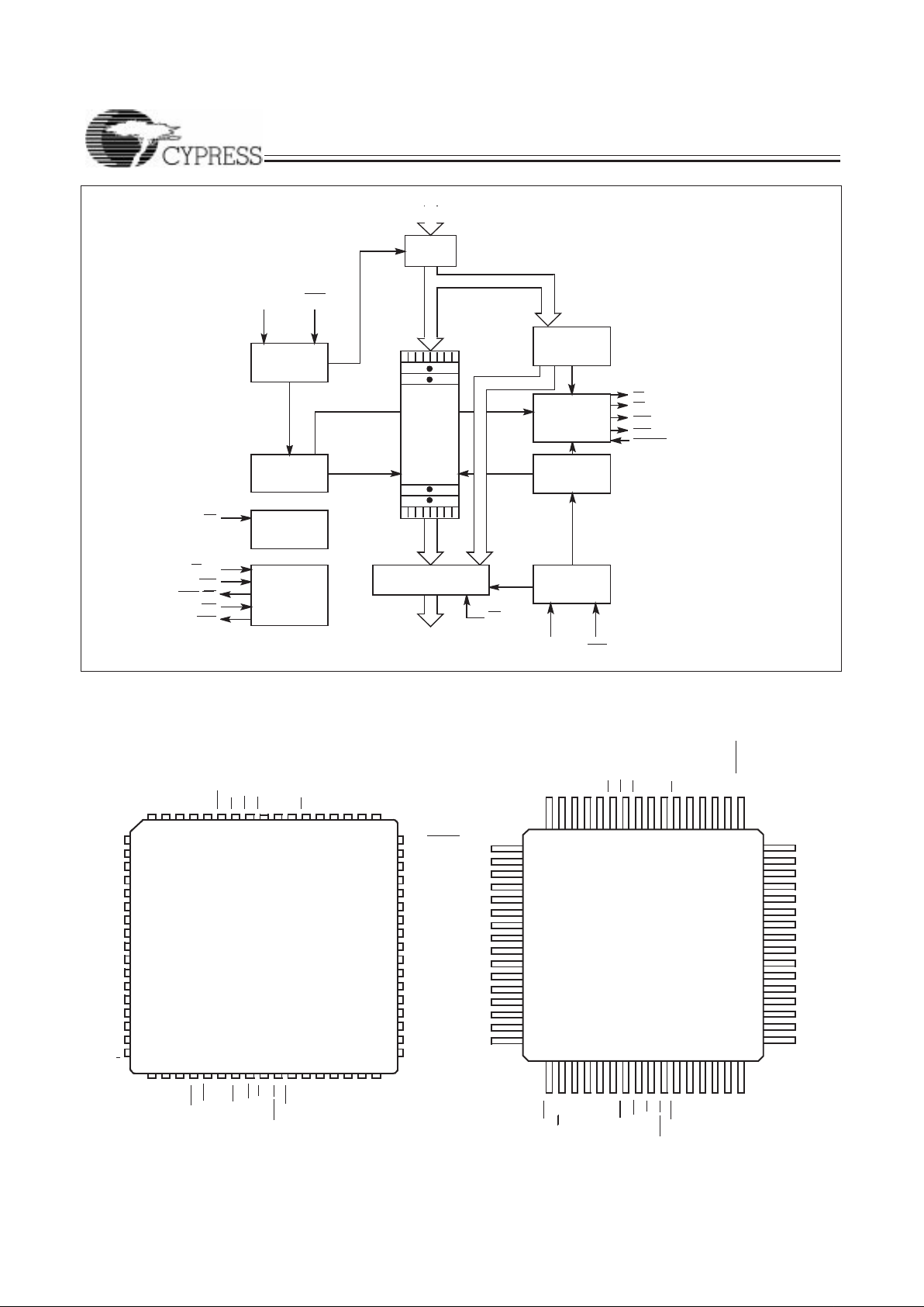
Logic Block Diagram
42X5–1
THREE–STATE
OUTPUT REGISTER
READ
CONTROL
FLAG
LOGIC
WRITE
CONTROL
WRITE
POINTER
READ
POINTER
RESET
LOGIC
EXPANSION
LOGIC
INPUT
REGISTER
FLAG
PROGRAM
REGISTER
D
0–17
RENRCLK
FF
EF
PAE
Q
0–17
WENWCLK
RS
FL/RT
WXI
OE
DUAL PORT
RAM ARRAY
64 x 18
256 x 18
512 x 18
1K x 18
2K x 18
4K x 18
PAF
WXO/HF
RXI
RXO
SMODE
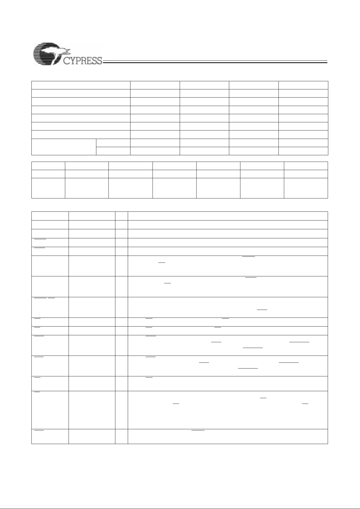
Pin Configurations
EF
10
11
12
13
14
15
16
17
18
19
20
21
22
23
24
67
Top View
60
59
58
57
56
55
54
53
52
51
50
49
48
3132 33 34 35 36 37 38 3940 4142 43
5 4 3 2 1 68 666564636261
Q
14
Q
13
GND
Q
12
Q
11
V
CC
Q
10
Q
9
GND
Q
8
Q
7
V
CC
D
14
D
13
D
12
D
11
D
10
D
9
V
CC
D
8
GND
D
7
D
6
D
5
D
4
2728 2930
987 6
47
46
45
44
Q
6
Q
5
GND
Q
4
D
3
D
2
D
1
D
0
25
26
VCC/SMODE
42x5–2
TQFP
Top View
42X5–3
1
2
3
4
5
6
7
8
9
10
11
12
13
14
15
48
47
46
45
44
43
42
41
40
39
38
37
36
35
34
33
17641863196220612160225923582457255626552754285329523051315032
49
16
PLCC
PAE
FL/RT
WCLK
WEN
WXI
VCCPAF
RXI
FF
WXO/HF
RXO
Q0Q
1
GND
Q2Q
3
V
CC
Q15GND
Q16Q17VCCEF
GND
VCCRS
OE
LD
REN
RCLK
GND
D17D16D
15
D
14
D
13
D
12
D
11
D
10
D
9
D
8
D
7
D
6
D
5
D
4
D
3
D
2
D
1
D
0
D
15
Q15GND
Q16Q
17
GND
VCCRS
OE
LD
REN
RCLK
GND
D17D
16
PAE
WCLK
WEN
WXI
V
CC
PAF
RXI
FF
WXO/HF
RXO
Q0Q
1
GND
Q2Q
3
Q
14
Q
13
GND
Q
12
Q
11
V
CC
Q
10
Q
9
GND
Q
8
Q
7
Q
6
Q
5
GND
Q
4
V
CC
V
CC
/SMODE
FL/RT
CY7C4425
CY7C4205
CY7C4215
CY7C4225
CY7C4235
CY7C4245
CY7C4425
CY7C4205
CY7C4215
CY7C4225
CY7C4235
CY7C4245
CY7C4425/4205/4215
CY7C4225/4235/4245
3
Selectio n Guide
7C42X5-10 7C42X5-15 7C42X5-25 7C42X5-35
Maximum Frequency (MHz) 100 66.7 40 28.6
Maximum Access Time (ns) 8 10 15 20
Minimum Cycle Time (ns) 10 15 25 35
Minimum Data or Enable Set-Up (ns) 3 4 6 7
Minimum Data or Enable Hold (ns) 0.5 1 1 2
Maximum Flag Delay (ns) 8 10 15 20
Operating Current (I
CC2
)
(mA) @ freq=20MHz
Commercial 45 45 45 45
Industrial 50 50 50 50
CY7C4425 CY7C4205 CY7C4215 CY7C4225 CY7C423 5 CY7C4245
Density 64 x 18 256 x 18 512 x 18 1K x 18 2K x 18 4K x 18
Packages 68-pin PLCC
64-pin TQFP
(10x10/14x14)
68-pin PLCC
64-pin TQFP
(10x10/14x14)
68-pin PLCC
64-pin TQFP
(10x10/14x14)
68-pin PLCC
64-pin TQFP
(10x10/14x14)
68-pin PLCC
64-pin TQFP
(10x10/14x14)
68-pin PLCC
64-pin TQFP
(10x10/14x14)
Pin Definitions
Signal Name Description I/O Function
D
0–17
Data Inputs I Data inputs for an 18-bit bus
Q
0–17
Data Outputs O Data outputs for an 18-bit bus
WEN Write Enable I Enables the WCLK input
REN Read Enable I Enables the RCLK input
WCLK Write Clock I T he rising edge clocks data into the FIFO when WEN is LOW and the FIFO is not
Full. When LD
is asserted, WCLK writes data into the programmable flag-offset
register.
RCLK Read Clock I The rising edge clocks data out of the FIFO when REN is LOW and the FIFO is not
Empty. When LD
is asserted, RCLK rea ds data out of the prog rammab le flag- off-
set register.
WXO/HF Write Expansion
Out/Half Full Flag
O Dual-Mode Pin:
Single device or width expansion - Half Full status flag.
Cascaded - Write Expansion Out signal, connected to WXI
of next device.
EF Empty Flag O When EF is LOW, the FIFO is empty. EF is synchronized to RCLK.
FF Full Flag O When FF is LO W, the F IF O i s fu ll. F F is synchronized to WCLK.
PAE Programmable
Almost Empty
O When PAE is LOW, the FIFO is almost empty based on the almost-empty offset
value programmed into the FIFO. PAE
is asyn chronous when VCC/SMODE is tied
to V
CC
; it is synchro nized to R CLK when VCC/SMODE is tied to VSS.
PAF Programm able
Almost Full
O When PAF is L O W, the F IF O is a lmost full ba s e d on the alm o st fu ll o ffse t va lu e
programmed into the FIFO. PAF
is asynchronous when VCC/SMODE is tied to
V
CC
; it is synchronized to WCLK when VCC/SMODE is tied to VSS.
LD Load I When LD is LO W, D
0 - 17
(O
0 - 17
) are written (read) into (from) the programma-
ble-flag-offset register.
FL/RT First Load/
Retransmit
I Dual-Mode Pin:
Cascaded - The first device in the daisy chain will have FL
tied to VSS; all other
devices will have FL
tied to VCC. In standard mode of width expansion, FL is tied
to V
SS
on all devices.
Not Cascaded - Tied to V
SS
. Retransmit function is also available in standalone
mode by strobing RT.
WXI Write Expansion
Input
I C ascaded - Connected to WXO of previous device.
Not Cascaded - Tied to V
SS
.
CY7C4425/4205/4215
CY7C4225/4235/4245
4
Maximum Ratings
(Above which the useful life may be impaired. For user guidelines, not tested.)
Storage Temperature ....................................−65
°C to +150° C
Ambient Temperature with
Power Applied.................................................−55
°C to +125° C
Supply Voltage to Ground Potential.... .............−0.5V to +7.0V
DC Voltage Applied to Outputs
in High Z State.....................................................−0.5V to +7.0V
DC Input Voltage.................................................−3.0V to +7.0V
Output Current into Outputs (LOW)............................. 20 mA
Static Discharge Voltage ...........................................>2001V
(per MIL-STD-883, Method 3015)
Latch-Up Current .....................................................>200 mA
RXI Read Expansion
Input
I C ascaded - Connected to RXO of previous device.
Not Cascaded - Tied to V
SS
.
RXO Read Expansion
Output
O Cascaded - Connected to RXI of next device.
RS Reset I Re sets device to empty condition. A reset is required before an initial read or write
operation after power-up.
OE Output Enable I When OE is LOW, the FIFO’s data outputs drive the bus to which they are con-
nected. If OE
is HIGH, the FIFO’s outputs are in High Z (high-impedance) state.
VCC/SMODE Synchronous
Almost Empty/
Almost Full Flags
I Dual-Mode Pin
Asynchronous Almost Empty/Almost Full flags - tied to V
CC
.
Synchronous Almost Empty/Almost Full flags - tied to V
SS
.
(Almost Empty s ync hro nized to R CLK, Almos t Fu ll synchr onize d to W C LK. )
Pin Definitions (continued)
Signal Name Description I/O Function
Operating Range
Range
Ambient
Temperatur e
V
CC
Commercial 0°C to +70°C 5V ± 10%
Industrial
[1]
−40°C to +85°C 5V ± 10%
Electrical Characteristics Over the Operating Range
[2]
Parameter Description Test Conditions
7C42X5-10 7C42X5-15 7C42X5-25 7C42X5-35
Min. Max. Min. Max. Min. Max. Min. Max. Unit
V
OH
Output HIGH Voltage VCC = Min.,
I
OH
= −2.0 mA
2.4 2.4 2.4 2.4 V
V
OL
Output LOW Voltage VCC = Min.,
I
OL
= 8.0 mA
0.4 0.4 0.4 0.4 V
V
IH
[3]
Input HIGH Voltage 2.2 V
CC
2.2 V
CC
2.2 V
CC
2.2 V
CC
V
V
IL
[3]
Input LOW Voltage −3.0 0.8 −3.0 0.8 −3.0 0.8 −3.0 0.8 V
I
IX
Input Leakage
Current
V
CC
= Max. −10 +10 −10 +10 −10 +10 −10 +10 µA
I
OS
[4]
Output Short
Circuit Current
VCC = Max.,
V
OUT
= GND
−90 −90 −90 −90 mA
I
OZL
I
OZH
Output OFF,
High Z Current
OE > VIH,
V
SS
< VO < V
CC
−10 +10 −10 +10 −10 +10 −10 +10 µA
I
CC2
[5]
Operating Current VCC = Max.,
I
OUT
= 0 mA
Com’l 45 45 45 45 mA
Ind 50 50 50 50 mA
I
SB
[6]
Standby Current VCC = Max.,
I
OUT
= 0 mA
Com’l 10 10 10 10 mA
Ind 15 15 15 15 mA
Notes:
1. T
A
is the “instant on” case temperature.
2. See the last page of this specification for Group A subgroup testing information.
3. The V
IH
and VIL specifications apply for all inputs except WXI, RXI. The WXI, RXI pin is not a TTL input. It is connected to either RXO, WXO of the
previous device or VSS.
4. Test no more than one output at a time for not more than one second.
5. Input signals switch from 0V to 3V with a rise/fall time less than 3 ns, clocks and clock enables switch at 20 MHz, while the data inputs switch at 10 MHz.
Outputs are unloaded.
6. All input signals are connected to V
CC
. All outputs are unloaded.
CY7C4425/4205/4215
CY7C4225/4235/4245
5
Notes:
7. Test ed initially and after any design or process changes that may affect these parameters.
8. C
L
= 30 pF for all AC parameters except for t
OHZ
.
9. CL = 5 pF for t
OHZ
.
Capacitance
[7]
Parameter Description Test Conditions Max. Unit
C
IN
Input Capacitance TA = 25°C, f = 1 MH z ,
V
CC
= 5.0 V
5 pF
C
OUT
Output Capacitance 7 pF
AC Test Loads and Waveforms
[8, 9]
3.0V
5V
OUTPUT
R11.1K
Ω
R2
680Ω
C
L
INCLUDING
JIGAND
SCOPE
GND
90%
10%
90%
10%
<3ns <3ns
OUTPUT 1.91V
Equivalen t to: THÉ EVENIN EQUIVALENT
42X5–4
410Ω
ALL INPUT PULSES
42X5–5
Switching Characteristics Over the Operating Range
Parameter Description
7C42X5-10 7C42X5-15 7C42X5-25 7C42X5-35
Min. Max. Min. Max. Min. Max. Min. Max. Unit
t
S
Clock Cycle Frequency 100 66.7 40 28.6 MHz
t
A
Data Access Time 2 8 2 10 2 15 2 20 ns
t
CLK
Clock Cycle Time 10 15 25 35 ns
t
CLKH
Clock HIGH Time 4.5 6 10 14 ns
t
CLKL
Clock LOW Time 4.5 6 10 14 ns
t
DS
Data Set-Up Time 3 4 6 7 ns
t
DH
Data Hold Time 0.5 1 1 2 ns
t
ENS
Enable Set-Up Time 3 4 6 7 ns
t
ENH
Enable Hold Time 0.5 1 1 2 ns
t
RS
Reset Pulse Width
[10]
10 15 25 35 ns
t
RSR
Reset Recovery Time 8 10 15 20 ns
t
RSF
Reset to Flag and Output Time 10 15 25 35 ns
t
PRT
Retransmit Pulse Width 12 15 25 35 ns
t
RTR
Retransmit Recovery Time 12 15 25 35 ns
t
OLZ
Output Enable to Output in Low Z
[11]
0 0 0 0 ns
t
OE
Output Enable to Output Valid 3 7 3 8 3 12 3 15 ns
t
OHZ
Output Enable to Output in High Z
[12]
3 7 3 8 3 12 3 15 ns
t
WFF
Write Clock to Full Flag 8 10 15 20 ns
t
REF
Read Clock to Empty Flag 8 10 15 20 ns
t
PAFasynch
Clock to Programmable Almost-Full Flag
[12]
(Asynchronous mode , VCC/SMODE tied to VCC)
12 16 20 25 ns
CY7C4425/4205/4215
CY7C4225/4235/4245
6
t
P A Fsyn ch
Clock to Programmable Almost-Full Flag
(Synchronous mode, V
CC
/SMODE tied to VSS)
8 10 15 20 ns
t
P A Easyn ch
Clock to Programmable Almost-Empty Flag
[12]
(Asynchronous mode, VCC/SMODE tied to VCC)
12 16 20 25 ns
t
PAEsynch
Clock to Programmable Almost-Full Flag
(Synchronous mode, V
CC
/SMODE tied to VSS)
8 10 15 20 ns
t
HF
Clock to Half-Full Flag 12 16 20 25 ns
t
XO
Clock to Expansion Out 7 10 15 20 ns
t
XI
Expansion in Pulse Width 3 6.5 10 14 ns
t
XIS
Expansion in Set-Up Time 4.5 5 10 15 ns
t
SKEW1
Skew Time between Read Clock and Write
Clock for Full Flag
5 6 10 12 ns
t
SKEW2
Skew Time between Read Clock and Write
Clock for Empty Flag
5 6 10 12 ns
t
SKEW3
Skew Time between Read Clock and Write
Clock for Programmable Almost Empty and Programmable Almost Full Flags.
10 15 18 20 ns
Switching Characteristics Over the Oper atin g Ran ge (contin ued)
Parameter Description
7C42X5-10 7C42X5-15 7C42X5-25 7C42X5-35
Min. Max. Min. Max. Mi n. Max. Min. Max. Unit
Switching Waveforms
Notes:
10. Pulse widths less than minimum values are not allowed.
11. Values guaranteed by design, not currently tested.
12.
PAF asyn ch
, t
PAEasynch
, after program reg ister w rite will not be v alid until 5 n s + t
PAF(E)
.
13. t
SKEW1
is the mi nimum t ime bet ween a r ising RCLK edg e and a ris ing WC LK edge to guar antee tha t F F will go HIGH during the current clock cycle. If the time between the
rising edge of R CLK and the r ising edge of WCLK is less than t
SKEW1
, then FF may not c hange state un til the ne xt WCLK edge .
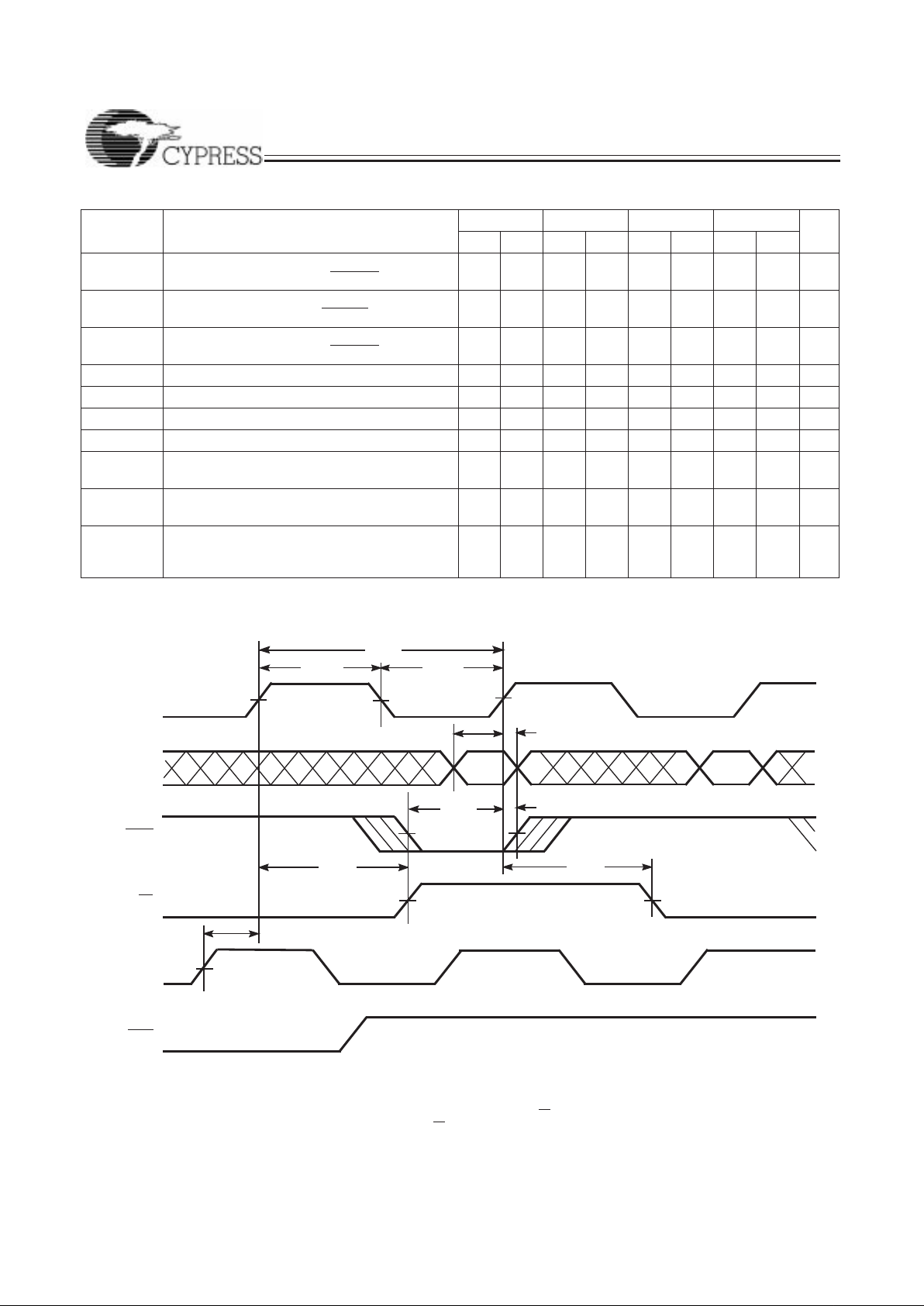
Write Cycle Timing
t
CLKH
t
CLKL
NO OPERATION
t
DS
t
SKEW1
t
ENS
WEN
t
CLK
t
DH
t
WFF
t
WFF
t
ENH
WCLK
D
0–D17
FF
REN
RCLK
42X5–6
[13]
CY7C4425/4205/4215
CY7C4225/4235/4245
7
Notes:
14. .t
SKEW2
is the minimum time between a rising WCLK edge and a rising RCL K edge to guarantee th at EF will go HIGH during the current clock cycle. It the time between the
rising edge of WCLK and th e risi ng ed ge of RCLK is les s than t
SKEW2
, then EF may not chan ge s tate unti l the next RC LK edge.
15. The clocks (RCLK, WCLK) can be free-running during reset.
16. After reset, the outputs will be LOW if OE
= 0 and three-st ate if OE = 1.
Switching Waveforms ( conti nued)
Read Cycle Timing
t
CLKH
t
CLKL
NO OPERATION
t
SKEW2
WEN
t
CLK
t
OHZ
t
REF
t
REF
RCLK
Q
0–Q17
EF
REN
WCLK
OE
t
OE
t
ENS
t
OLZ
t
A
t
ENH
VALID DATA
42X5–7
[14]
t
RS
t
RSR
Q0-Q
17
RS
t
RSF
t
RSF
t
RSF
OE=1
OE=0
REN
,WEN,
LD
EF,PAE
FF,PAF,
HF
42X5–8
Reset Timing
[15]
[16]

CY7C4425/4205/4215
CY7C4225/4235/4245
8
Notes:
17. When t
SKEW2
> minimum specification, t
FRL
(maximum) = t
CLK
+ t
SKEW2
. When t
SKEW2
< minimum specific ation, t
FRL
(maximum) = either 2*t
CLK
+ t
SKEW2
or t
CLK
+ t
SKEW2
.
The Latency T im ing appli es only at the Empt y Boundar y (EF = L OW) .
18. The first word is available the cycle after EF goes H IGH, alw ays.
Switching Waveforms ( conti nued)
D
0
(FIRSTVALIDWRITE)
First Data Word Latency after Reset with Simultaneous Read and Write
t
SKEW2
WEN
WCLK
Q
0–Q17
EF
REN
OE
t
OE
t
ENS
t
OLZ
t
DS
RCLK
t
REF
t
A
t
FRL
D
1
D
2
D
3
D
4
D
0
D
1
D0–D
17
42X5–9
t
A
[18]
[17]
D1D0
t
ENS
t
SKEW2
Empty Flag Timing
WEN
WCLK
Q
0–Q17
EF
REN
OE
t
DS
t
ENH
RCLK
t
REF
t
A
t
FRL
D0–D
17
D0
t
SKEW2
t
FRL
t
REF
t
DS
t
ENS
t
ENH
42X5–10
t
REF
[17]
[17]

CY7C4425/4205/4215
CY7C4225/4235/4245
9
Switching Waveforms ( conti nued)
NEXT DATA READ
DATA WRITE
NO WRITE
DATA IN OUTPUT REGISTER
Full Flag Timing
FF
WCLK
Q
0–Q17
REN
OE
RCLK
t
A
D0–D
17
DATAREAD
t
SKEW1
t
DS
t
ENS
t
ENH
WEN
t
WFF
t
A
t
SKEW1
t
ENS
t
ENH
t
WFF
DATA WRITE
NO WRITE
t
WFF
LOW
42X5–11
[13]
[13]
t
ENH
Half-Full FlagTiming
WCLK
HF
REN
RCLK
t
CLKH
t
HF
t
ENS
HALF FULL+1
OR MORE
t
CLKL
t
ENS
HALF FULLORLESS HALF FULLORLESS
t
HF
42X5–12
WEN

CY7C4425/4205/4215
CY7C4225/4235/4245
10
Notes:
19. PAE offset – n. Number of data words into FIFO already = n.
20. PAE offset – n.
21. t
SKEW3
is the minimum time between a risi ng WCLK and a rising RCLK edge for P AE to change state during t hat clock cycle. If the time between the edg e of WCLK and the
rising RCLK is less t han t
SKEW3
, then PAE may not change state unti l the next R CLK.
22. If a read is performed on this rising edge of the read clock, there will be Empty + (n – 1) words in the FIFO when PAE
goes LOW .
Switching Waveforms ( conti nued)
t
ENH
Programmable Almost Empty
Flag
Timing
WCLK
PAE
]
REN
RCLK
t
CLKH
t
PAE
t
ENS
n+1 WORDS
IN FIFO
t
CLKL
t
ENS
t
PAE
n WORDS IN FIFO
42X5–13
[19]
WEN
Note
t
ENH
WCLK
PAE
RCLK
t
CLKH
t
ENS
t
CLKL
t
ENS
t
PAEsynch
N + 1 WORDS
INFIFO
42X5–14
t
ENH
t
ENS
t
ENH
t
ENS
t
PAEsynch
REN
WEN
WEN2
t
SKEW3
Note
Programmable Almost Empty Flag Timing (applies only in SMODE (SMODE is LOW)
[21]
22
20

CY7C4425/4205/4215
CY7C4225/4235/4245
11
Notes:
23. PAF offset = m. Number of data words written into FIFO already = 64 – m + 1 for the CY7C4425, 256 – m + 1 for the CY7C4205, 512 – m + 1 for the
CY7C4215. 1024 – m + 1 for the CY7C4225, 2048 – m + 1 for the CY7C4235, and 4096 – m + 1 for the CY7C4245.
24. PAF is offset = m.
25. 64 – m words in CY7C4425, 256 – m words inCY7C4205, 512 – m word in CY7C4215. 1024 – m words in CY7C4225, 2048 – m words in CY7C4235, and
4096 – m words in CY7C4245.
26. 64 – m + 1 words in CY7C4425, 256 – m + 1 words in CY7C4205, 512 – m +1 words in CY7C4215, 1024 – m + 1 CY7C4225, 2048 – m + 1 in CY74235,
and 4096 – m + 1 words in CY7C4245.
27. If a write is performed on this rising edge of the write clock, there will be Full – (m – 1) words of the FIFO when PAF
goes LOW .
28. PAF offset = m.
29. 64 – m words in CY7C4425, 256 – m words in FIFO for CY7C4205, 512 – m word in CY7C4215. 1024 – m words in CY7C4225, 2048 – m words in CY7C4235,
and 4096 – m words in CY7C4245.
30. t
SKEW3
is the minimum time between a rising RCLK and a rising WCLK edge for P AF to c han ge sta te d uring that c loc k cy cle. If th e t ime bet ween the edge of RCLK and the
rising edge of W CLK is l ess tha n t
SKEW3
, then PAF may not change state unt il the nex t WCLK rising edge.
Switching Waveforms ( conti nued)
Note
t
ENH
WEN
WCLK
REN
RCLK
t
CLKH
t
PAF
t
ENS
t
CLKL
t
ENS
t
PAF
42X5–15
FULL − M WORDS
IN FIFO
FULL − M + 1 WORDS
IN FIFO
Programmable Almost Full Flag Timing
[26]
PAF
[24]
23
[25]
Note
Note
t
ENH
WCLK
PAF
RCLK
t
CLKH
t
ENS
FULL − M WORDS
IN FIFO
t
CLKL
t
ENS
FULL- M+1Ω ORDS
INFIFO
42X5–16
t
ENH
t
ENS
t
ENH
t
ENS
t
PAF
REN
WEN2
t
SKEW3
t
PAFsynch
[30]
28
27
WEN
Programmable Almost Full Flag Timing (applies only in SMODE (SMODE in LOW))
[29]

CY7C4425/4205/4215
CY7C4225/4235/4245
12
Note:
31. Write to Last Physical Location.
Switching Waveforms ( conti nued)
t
ENH
Write Programmable Registers
LD
WCLK
t
CLKH
t
ENS
t
CLKL
PAE OFFSET
D
0–D17
WEN
t
ENS
PAF OFFSET
PAE OFFSET
t
CLK
D0–D
11
t
DS
t
DH
42X5–17
t
ENH
Read Pr ogrammable R egisters
LD
RCLK
t
CLKH
t
ENS
t
CLKL
PAE OFFSET
Q
0–Q17
WEN
t
ENS
PAF OFFSET PAE OFFSET
t
CLK
UNKNOWN
t
A
42X5–18
Write Expansion Out Timing
WEN
WCLK
WXO
t
CLKH
t
ENS
Note
t
XO
t
XO
42X5–19
31

CY7C4425/4205/4215
CY7C4225/4235/4245
13
Notes:
32. Read from Last Physical Location.
33. Clocks are free running in this case.
34. The flags may change state during Retransmit as a result of the offset of the read and write pointers, but flags will be valid at t
RTR
.
35. For the synchronous PAE and PAF flags ( SMODE), an appropr iate c lock cycle is necess ary after t
RTR
to update these f lags.
Switching Waveforms ( conti nued)
Read Expansion Out Timing
REN
WCLK
RXO
t
CLKH
t
ENS
Note
t
XO
t
XO
42X5–20
32
Write Expansion In Tim ing
WCLK
WXI
t
XI
t
XIS
42X5–21
Read Expansion In Timing
RCLK
RXI
t
XI
t
XIS
42X5–22
Retransmit Timing
REN/WEN
FL/RT
t
PRT
t
RTR
42X5–23
EF/FF
and all
async flags
HF/PAE/PAF
[33, 34, 35]

CY7C4425/4205/4215
CY7C4225/4235/4245
14
Architectur e
The CY7C42X5 consists of an array of 64 to 4K words of 18
bits each (implemented by a dual-port array of SRAM cells), a
read pointer, a write pointer, control sig nals (RCLK, WCLK,
REN
, WEN, RS), and flags (EF, PAE, HF, PAF, FF). The
CY7C42X5 also includes the control signals WXI
, RXI, WXO,
RXO
for depth expansion.
Resetting the FIFO
Upon power-up, the FIFO must b e reset with a Reset (RS)
cycle. This causes the FIFO to enter the Empty condition signified by EF
being LOW. All data outputs go LOW after the
falling edge of RS
only if OE is asserted. In order for the FIFO
to reset to its default state, a falli ng edge must occur on RS
and the user must not read or write while RS is LOW.
FIFO Operation
When the WEN signal is active (LOW), data present on the
D
0–17
pins is written into the FIFO on each rising ed ge of the
WCLK signal. Similarly, when the REN
signal is active LOW,
data in the FIFO memory will be presented on the Q
0–17
outputs. New data will be presented o n eac h rising edge of RCLK
while REN
is active LOW and OE is LOW. REN must set up
tENS before RCLK for it to be a valid read function. WEN
must
occur tENS before WCLK for it to be a valid write function.
An outpu t enable (OE
) pin is provided to three-state the Q
0–17
outputs when OE is deass e rted. When OE is enabled (LOW),
data in the output register will be available to the Q
0–17
outputs
after t
OE
. If devices are cascaded, the OE function will only
output data on the FIFO that is read enabled.
The FIFO contains overflow circuitry to disallow additional
writes when the FIFO is full, and underflow circuitry to disallow
additional reads when the FIFO is empty. An empty FIFO
maintains the data of the last valid read on i ts Q
0–17
outputs
even after additional reads occur.
Programming
The CY7C42X5 devices contain two 12-bit offset registers.
Data present on D
0– 11
during a program write wi ll determine
the distance from Empty (Full) that the Almost Empty (Almost
Full) flags become active. If the user elects not to program the
FIFO’s flags, the default offset values are used (see
Table 2
).
When the Load LD
pin is set LOW and WEN is set LOW, data
on the inputs D
0–11
is written into the Empty offset register on
the first LOW-to-H IGH transition of the writ e clock (WCLK).
When the LD
pin and WEN are held LOW then data is written
into the Full offset register on the second LOW-to-HIGH transition of the write clock (WCLK). The third transition of the write
clock (WCLK) again writes to the Empty offset register ( see
Ta ble 1
). Writing all offset registers does not have to occur at
one time. One or two offset registers can be written and then,
by bringing the LD
pin HIGH, the FIFO is r eturned to normal
read/write operation. Wh en the L D
pin is set LOW, and WEN
is LOW, the next offset register in sequence is written.
The contents of the offset registers can be read on the output
lines when the LD
pin is set LOW and REN is set LOW; then,
data can be read on the LOW-to-HIGH transition of the re ad
clock (RCLK).
Flag Operation
The CY7C42X5 devices provide five flag pins to indicate the
condition of the FIFO contents. Empty and Full are synchronous. PAE
and PAF are synchronous if VCC/SMODE is tied to
V
SS
.
Full Flag
The Full Flag (FF
) will go LOW when device is Full. Write op-
erations are inhibited whenever FF
is LOW regardless of the
state of WEN
. FF is synchronize d to WCL K, i.e., it is exclusiv e-
ly updated by each rising edge of WCLK.
Empty Flag
The Empty Flag (EF
) will go LOW when the device is empty.
Read operations are inhibited whenever EF
is LOW, regard-
less of the state of REN
. EF is synchronized to RCLK, i.e., it is
exclusively updated by each rising edge of RCLK.
Programmable Almost Empty/Al most Ful l Flag
The CY7C42X5 features programmable Almost Empty and Almost Full Flags. Each flag can be programmed (described in
the Programming section) a specific distance from the corresponding bound a ry flags (Empty or Full). When the FIFO contains the number of words or fewer for which the flags have
been programmed, the P AF
or P AE will be asserted, signifying
that the FIFO is either Almost Full or Almost Empty. See
Table
2
for a description of programmable flags.
When the SMODE
pin is tied LOW, the PA F flag signal transition is caused by the rising edge of the write clock and the PAE
flag transition is caused by the rising edge of the read clock.
Retransmit
The retransmit feature is beneficial when transferring packets
of data. It enables the receipt of data to be acknowledged by
the receiver and retransmitted if necessary.
The Retransmit (RT) input is active in the standalone and width
expansion modes. The retransmi t feature is intended for use
when a number of writes equal to or less than the depth of the
FIFO have occurred since the last RS
cycle. A HIGH pulse on
RT resets the internal read pointer to the first physical location
of the FIFO. WCLK and RCLK may be free running but must
be disabled during and t
RTR
after the retransmit pulse. With
Table 1. Write Offset Register
LD
WEN WCLK
[36]
Selection
0 0 Writing to offset registers:
Empty Offset
Full Offset
0 1 No Operation
1 0 Write Into FIFO
1 1 No Operation
Note:
36. The same selection sequence applies to reading from the registers. RE N
is enabled and read is p erformed on th e LOW- to-HIGH t ransition of RC LK.

CY7C4425/4205/4215
CY7C4225/4235/4245
15
every valid read cycle after retransmit, previously accessed
data is read and the read pointer is inc remented until i t is equal
to the write pointer. Flags are governed by the relative locations of the read and write pointers and are updated during a
retransmit cycle. Data written to the FIFO after activation of RT
are transmitted also.
The full depth of the FIFO can be repeatedly retransmitted.
Width Expansion Configuration
The CY7C42X5 can be expanded in width to provide word
widths greater than 18 in increments of 18. During width expansion mode all control line inputs are comm on and all flags
are available. Empty (Full) flags should be created by ANDing
the Empty (Full) flags of every FIFO. This technique will avoid
ready data from the FIFO that is “staggered” by one clock cycle
due to the variations in skew between RCLK and WCLK.
Figure 1
demonstrates a 36-word width by using two CY7C42X5.
Table 2. Flag Truth Table.
Number of Words in FIFO
FF PAF HF PAE EF7C4425 - 64 x 18 7C4205 - 256 x 18 7C4215 - 512 x 18
0 0 0 H H H L L
1 to n
[37
1 to n
[37]
1 to n
[37]
H H H L H
(n+1) to 32 (n+1) to 128 (n+1) to 256 H H H H H
33 to (64 – (m+1)) 129 to (256 – (m+1)) 257 to (512 – (m+1)) H H L H H
(64 – m)
[38]
to 63 (256 – m)
[38]
to 255 (512 – m)
[38]
to 51 1 H L L H H
64 256 512 L L L H H
Number of Words in FIFO
FFPAFHFPAEEF 7C4225 - 1K x 18 7C4235 - 2K x 18 7C4245 - 4K x 18
000 HHHLL
1 to n
[37]
1 to n
[37]
1 to n
[37]
HHH LH
(n+1) to 512 (n+1) to 1024 (n+1) to 2048 H H H H H
513 to (1024 – (m+1)) 1025 to (2048 – (m+1)) 2049 to (4096 – (m+1)) H H L H H
(1024 – m)
[38]
to 1023 (2048 – m)
[38]
to 2047 (4096 – m)
[38]
to 4095 H L L H H
1024 2048 4096 L L L H H
Notes:
37. n = Empty Offset (Default Values: CY7C4425 n = 7, CY7C4205 n = 31, CY7C4215 n = 63, CY7C4225/7C4235/7C4245 n = 127).
38. m = Full Offset (Default Values: CY7C4425 n = 7, CY7C4205 n = 31, CY7C4215 n = 63, CY7C4225/7C4235/7C4245 n = 127).
Figure 1. Block Diagram of 64x36/256 x 36/512 x 36/1024 x 36/2048 x 36/4096 x 36 Synchronous FIFO Memory Used in a
Width Expansion Configuration.
42X5–24
FF
FF EF
EF
WRITECLOCK (WCLK)
WRITEENABLE (WEN
)
LOAD(LD
)
PROGRAMMABLE(PAE
)
HALFFULLFLAG(HF
)
FULLFLAG(FF
)
7C4425
7C4205
7C4215
7C4225
7C4235
7C4235
7C4425
7C4205
7C4215
7C4225
7C4235
7C4235
1836
DATAIN (D)
RESET
(RS)
18
RESET(RS)
READCLOCK(RCLK)
READENABLE(REN
)
OUTPUTENABLE(OE
)
PROGRAMMABLE(PAF
)
EMPTYFLAG
(EF)
18
DATAOUT(Q)
18 36
FIRST LOAD(FL)
WRITE EXPANSION IN (WXI
)
READ EXPANSION IN (RXI
)

CY7C4425/4205/4215
CY7C4225/4235/4245
16
Depth Expansion Configuration
(with Programmab le Flags)
The CY7C42X5 can easily be adapted to applications requiring more than 64/256/512/1024/2048/4096 words of buffering.
Figure 2
shows Depth Expansion using t hree CY7C42X5s. Maxi-
mum depth is limited only by signal loading. Follow these steps:
1. The first device must be desig nated by grounding the First
Load (FL
) control input.
2. All other devices must have FL
in t h e HIGH st a t e.
3. The Write Expansion Out (WXO
) pin of each device must be
tied to the Write Expansion In (WXI
) pin of the next device.
4. The Read Expansion Out (RXO
) pin of each device must be
tied to the Read Expansion In (RXI
) pin of the next device.
5. Al l Load (LD
) pins are tied together.
6. The Half-Full Flag (HF
) is not available in the Depth Expansion
Configuration.
7. EF
, FF, PAE, and PAF are created with composite flags by
ORing together these respective flags for monitoring. The
composite PAE
and PAF flags are not precise.
Figure 2. Bl ock Diagram of 192 x 18/768 x 18/1536 x 18/3072 x 18/12288 x 18 Synchronous FIFO Memory
with Programmable Flags used in Depth Expansion Configuration.
42X5–23
WRITECLOCK(WCLK)
WRITE ENABLE
(WEN)
RESET
(RS)
LOAD
(LD)
FF
PAF
PAF
FF EF
PAE
PAE
EF
WXI RXI
FIRSTLOAD(FL)
READ CLOCK
(RCLK)
READ ENABLE
(REN)
OUTPUT ENABLE
(OE)
WXO
RXO
7C4425
7C4205
7C4215
7C4225
7C4235
7C4235
PAF
FF EF
PAE
WXI RXI
WXO RXO
7C4425
7C4205
7C4215
7C4225
7C4235
7C4235
V
CC
FIRSTLOAD(FL)
PAF
FF EF
PAE
WXI RXI
WXO RXO
7C4425
7C4205
7C4215
7C4225
7C4235
7C4235
V
CC
FIRSTLOAD(FL)
DATAIN
(D) DATAOUT (Q)

CY7C4425/4205/4215
CY7C4225/4235/4245
17
T y pical AC and DC Characteristics
SUPPLY VOLTAGE (V)
NORMALIZED t
A
vs.SUPPLY
VOLTAGE
NORMALIZED SUPPLY CURRENT
vs. SUPPLY VOLTAGE
NORMALIZED t
A
vs.
AMBIENT TEMPERATURE
NORMALIZED SUPPLY CURRENT
vs. AMBIENT TEMPERATURE
FREQUENCY (MHz)
NORMALIZED SUPPLY CURRENT
vs. FREQUENCY
SUPPLY VOLTAGE
(V)
V
CC
=5.0V
NORMALIZED I
CC
NORMALIZED I
CC
AMBIENT TEMPERATURE(°C)
V
IN
=3.0V
T
A
=25°C
f=100 MHz
V
IN
=3.0V
V
CC
=5.0V
f=100 MHz
NORMALIZED I
CC
VCC=5.0V
T
A
=25°C
V
IN
=3.0V
CAPACITANCE(pF)
NORMALIZED t
A
TYPICAL tACHANGE vs.
OUTPUT
LOADING
V
CC
=5.0V
T
A
=25°C
OUTPUT SOURCECURRENT
vs. OUTPUT VOLTAGE
OUTPUT VOLTAGE
(V)
OUTPUT SINK CURRENTvs.
OUTPUT VOLTAGE
OUTPUT VOLTAGE(V)
OUTPUTS OURCE CURRENT (mA)
OUTPUT SINK CURENT (mA)
NORMALIZED t
A
AMBIENT TEMPERATURE
NORMALIZED t
A
4
4.5
5
5.5 6
0.6
0.8
1.0
1.2
1.4
−55 25 125
0.8
0.9
1.0
1.1
1.2
0255075100
0.6
0.7
0.8
0.9
1.0
1.1
0.8
0.9
1.0
1.1
1.2
4
4.5 5 5.5
6
−55 25 125
0.5
.75
1.0
1.25
1.50
T
A
=25°C
.50 275 550 825 1000
−5.0
10
25
40
25
35
45
55
012345
01234
0
20
40
60
80
100
120
140
120
T
A
=25°C
V
CC
=5.0V
T
A
=25°C
V
CC
=5.0V
(°C)

CY7C4425/4205/4215
CY7C4225/4235/4245
18
Ordering Info rma tio n
64 x 18 Synchronous FIFO
Speed
(ns) Ordering Code
Package
Name
Package
Type
Operating
Range
10 CY7C4425-10AC A65 64-Lead 14x14 Thin Quad Flatpack Commercial
CY7C4425-10ASC A64 64-Lead 10x10 Thin Quad Flatpack
CY7C4425-10JC J81 68-Lead Plastic Leaded Chip Carrier
CY7C4425-10AI A65 64-Lead 14x14 Thin Quad Flatpack Industrial
CY7C4425-10ASI A64 64-Lead 10x10 Thin Quad Flatpack
CY7C4425-10JI J81 68-Lead Plastic Leaded Chip Carrier
15 CY7C4425-15AC A65 64-Lead 14x14 Thin Quad Flatpack Commercial
CY7C4425-15ASC A64 64-Lead 10x10 Thin Quad Flatpack
CY7C4425-15JC J81 68-Lead Plastic Leaded Chip Carrier
CY7C4425-15AI A65 64-Lead 14x14 Thin Quad Flatpack Industrial
CY7C4425-15ASI A64 64-Lead 10x10 Thin Quad Flatpack
CY7C4425-15JI J81 68-Lead Plastic Leaded Chip Carrier
25 CY7C4425-25AC A65 64-Lead 14x14 Thin Quad Flatpack Commercial
CY7C4425-25ASC A64 64-Lead 10x10 Thin Quad Flatpack
CY7C4425-25JC J81 68-Lead Plastic Leaded Chip Carrier
CY7C4425-25AI A65 64-Lead 14x14 Thin Quad Flatpack Industrial
CY7C4425-25ASI A64 64-Lead 10x10 Thin Quad Flatpack
CY7C4425-25JI J81 68-Lead Plastic Leaded Chip Carrier
35 CY7C4425-35AC A65 64-Lead 14x14 Thin Quad Flatpack Commercial
CY7C4425-35ASC A64 64-Lead 10x10 Thin Quad Flatpack
CY7C4425-35JC J81 68-Lead Plastic Leaded Chip Carrier
CY7C4425-35AI A65 64-Lead 14x14 Thin Quad Flatpack Industrial
CY7C4425-35ASI A64 64-Lead 10x10 Thin Quad Flatpack
CY7C4425-35JI J81 68-Lead Plastic Leaded Chip Carrier

CY7C4425/4205/4215
CY7C4225/4235/4245
19
256 x 18 Synchronous FIFO
Speed
(ns) Ordering Code
Package
Name
Package
Type
Operating
Range
10 CY7C4205-10AC A65 64-Lead 14x14 Thin Quad Flatpack Commercial
CY7C4205-10ASC A64 64-Lead 10x10 Thin Quad Flatpack
CY7C4205-10JC J81 68-Lead Plastic Leaded Chip Carrier
CY7C4205-10AI A65 64-Lead 14x14 Thin Quad Flatpack Industrial
CY7C4205-10ASI A64 64-Lead 10x10 Thin Quad Flatpack
CY7C4205-10JI J81 68-Lead Plastic Leaded Chip Carrier
15 CY7C4205-15AC A65 64-Lead 14x14 Thin Quad Flatpack Commercial
CY7C4205-15ASC A64 64-Lead 10x10 Thin Quad Flatpack
CY7C4205-15JC J81 68-Lead Plastic Leaded Chip Carrier
CY7C4205-15AI A65 64-Lead 14x14 Thin Quad Flatpack Industrial
CY7C4205-15ASI A64 64-Lead 10x10 Thin Quad Flatpack
CY7C4205-15JI J81 68-Lead Plastic Leaded Chip Carrier
25 CY7C4205-25AC A65 64-Lead 14x14 Thin Quad Flatpack Commercial
CY7C4205-25ASC A64 64-Lead 10x10 Thin Quad Flatpack
CY7C4205-25JC J81 68-Lead Plastic Leaded Chip Carrier
CY7C4205-25AI A65 64-Lead 14x14 Thin Quad Flatpack Industrial
CY7C4205-25ASI A64 64-Lead 10x10 Thin Quad Flatpack
CY7C4205-25JI J81 68-Lead Plastic Leaded Chip Carrier
35 CY7C4205-35AC A65 64-Lead 14x14 Thin Quad Flatpack Commercial
CY7C4205-35ASC A64 64-Lead 10x10 Thin Quad Flatpack
CY7C4205-35JC J81 68-Lead Plastic Leaded Chip Carrier
CY7C4205-35AI A65 64-Lead 14x14 Thin Quad Flatpack Industrial
CY7C4205-35ASI A64 64-Lead 10x10 Thin Quad Flatpack
CY7C4205-35JI J81 68-Lead Plastic Leaded Chip Carrier

CY7C4425/4205/4215
CY7C4225/4235/4245
20
512 x 18 Synchronous FIFO
Speed
(ns) Ordering Code
Package
Name
Package
Type
Operating
Range
10 C Y7C4215-10AC A65 64-Lead 14x14 Thin Quad Flatpack Commercial
CY7C4215-10ASC A64 64-Lead 10x10 Thin Quad Flatpack
CY7C4215-10JC J81 68-Lead Plastic Leaded Chip Carrier
CY7C4215-10AI A65 64-Lead 14x14 Thin Quad Flatpack Industrial
CY7C4215-10ASI A64 64-Lead 10x10 Thin Quad Flatpack
CY7C4215-10JI J81 68-Lead Plastic Leaded Chip Carrier
15 C Y7C4215-15AC A65 64-Lead 14x14 Thin Quad Flatpack Commercial
CY7C4215-15ASC A64 64-Lead 10x10 Thin Quad Flatpack
CY7C4215-15JC J81 68-Lead Plastic Leaded Chip Carrier
CY7C4215-15AI A65 64-Lead 14x14 Thin Quad Flatpack Industrial
CY7C4215-15ASI A64 64-Lead 10x10 Thin Quad Flatpack
CY7C4215-15JI J81 68-Lead Plastic Leaded Chip Carrier
25 C Y7C4215-25AC A65 64-Lead 14x14 Thin Quad Flatpack Commercial
CY7C4215-25ASC A64 64-Lead 10x10 Thin Quad Flatpack
CY7C4215-25JC J81 68-Lead Plastic Leaded Chip Carrier
CY7C4215-25AI A65 64-Lead 14x14 Thin Quad Flatpack Industrial
CY7C4215-25ASI A64 64-Lead 10x10 Thin Quad Flatpack
CY7C4215-25JI J81 68-Lead Plastic Leaded Chip Carrier
35 C Y7C4215-35AC A65 64-Lead 14x14 Thin Quad Flatpack Commercial
CY7C4215-35ASC A64 64-Lead 10x10 Thin Quad Flatpack
CY7C4215-35JC J81 68-Lead Plastic Leaded Chip Carrier
CY7C4215-35AI A65 64-Lead 14x14 Thin Quad Flatpack Industrial
CY7C4215-35ASI A64 64-Lead 10x10 Thin Quad Flatpack
CY7C4215-35JI J81 68-Lead Plastic Leaded Chip Carrier

CY7C4425/4205/4215
CY7C4225/4235/4245
21
1K x 18 Synchronous FIFO
Speed
(ns) Ordering Code
Package
Name
Package
Type
Operating
Range
10 CY7C4225-10AC A65 64-Lead 14x14 Thin Quad Flatpack Commercial
CY7C4225-10ASC A64 64-Lead 10x10 Thin Quad Flatpack
CY7C4225-10JC J81 68-Lead Plastic Leaded Chip Carrier
CY7C4225-10AI A65 64-Lead 14x14 Thin Quad Flatpack Industrial
CY7C4225-10ASI A64 64-Lead 10x10 Thin Quad Flatpack
CY7C4225-10JI J81 68-Lead Plastic Leaded Chip Carrier
15 CY7C4225-15AC A65 64-Lead 14x14 Thin Quad Flatpack Commercial
CY7C4225-15ASC A64 64-Lead 10x10 Thin Quad Flatpack
CY7C4225-15JC J81 68-Lead Plastic Leaded Chip Carrier
CY7C4225-15AI A65 64-Lead 14x14 Thin Quad Flatpack Industrial
CY7C4225-15ASI A64 64-Lead 10x10 Thin Quad Flatpack
CY7C4225-15JI J81 68-Lead Plastic Leaded Chip Carrier
25 CY7C4225-25AC A65 64-Lead 14x14 Thin Quad Flatpack Commercial
CY7C4225-25ASC A64 64-Lead 10x10 Thin Quad Flatpack
CY7C4225-25JC J81 68-Lead Plastic Leaded Chip Carrier
CY7C4225-25AI A65 64-Lead 14x14 Thin Quad Flatpack Industrial
CY7C4225-25ASI A64 64-Lead 10x10 Thin Quad Flatpack
CY7C4225-25JI J81 68-Lead Plastic Leaded Chip Carrier
35 CY7C4225-35AC A65 64-Lead 14x14 Thin Quad Flatpack Commercial
CY7C4225-35ASC A64 64-Lead 10x10 Thin Quad Flatpack
CY7C4225-35JC J81 68-Lead Plastic Leaded Chip Carrier
CY7C4225-35AI A65 64-Lead 14x14 Thin Quad Flatpack Industrial
CY7C4225-35ASI A64 64-Lead 10x10 Thin Quad Flatpack
CY7C4225-35JI J81 68-Lead Plastic Leaded Chip Carrier

CY7C4425/4205/4215
CY7C4225/4235/4245
22
2K x 18 Synchronous FIFO
Speed
(ns) Ord ering Code
Package
Name
Package
Type
Operating
Range
10 CY7C4235-10AC A65 64-Lead 14x14 Thin Quad Flatpack Commercial
CY7C4235-10ASC A64 64-Lead 10x10 Thin Quad Flatpack
CY7C4235-10JC J81 68-Lead Plastic Leaded Chip Carrier
CY7C4235-10AI A65 64-Lead 14x14 Thin Quad Flatpack Industrial
CY7C4235-10ASI A64 64-Lead 10x10 Thin Quad Flatpack
CY7C4235-10JI J81 68-Lead Plastic Leaded Chip Carrier
15 CY7C4235-15AC A65 64-Lead 14x14 Thin Quad Flatpack Commercial
CY7C4235-15ASC A64 64-Lead 10x10 Thin Quad Flatpack
CY7C4235-15JC J81 68-Lead Plastic Leaded Chip Carrier
CY7C4235-15AI A65 64-Lead 14x14 Thin Quad Flatpack Industrial
CY7C4235-15ASI A64 64-Lead 10x10 Thin Quad Flatpack
CY7C4235-15JI J81 68-Lead Plastic Leaded Chip Carrier
25 CY7C4235-25AC A65 64-Lead 14x14 Thin Quad Flatpack Commercial
CY7C4235-25ASC A64 64-Lead 10x10 Thin Quad Flatpack
CY7C4235-25JC J81 68-Lead Plastic Leaded Chip Carrier
CY7C4235-25AI A65 64-Lead 14x14 Thin Quad Flatpack Industrial
CY7C4235-25ASI A64 64-Lead 10x10 Thin Quad Flatpack
CY7C4235-25JI J81 68-Lead Plastic Leaded Chip Carrier
35 CY7C4235-35AC A65 64-Lead 14x14 Thin Quad Flatpack Commercial
CY7C4235-35ASC A64 64-Lead 10x10 Thin Quad Flatpack
CY7C4235-35JC J81 68-Lead Plastic Leaded Chip Carrier
CY7C4235-35AI A65 64-Lead 14x14 Thin Quad Flatpack Industrial
CY7C4235-35ASI A64 64-Lead 10x10 Thin Quad Flatpack
CY7C4235-35JI J81 68-Lead Plastic Leaded Chip Carrier

CY7C4425/4205/4215
CY7C4225/4235/4245
23
4K x 18 Synchronous FIFO
Speed
(ns) Ordering Code
Package
Name
Package
Type
Operating
Range
10 CY7C4245-10AC A65 64-Lead 14x14 Thin Quad Flatpack Commercial
CY7C4245-10ASC A64 64-Lead 10x10 Thin Quad Flatpack
CY7C4245-10JC J81 68-Lead Plastic Leaded Chip Carrier
CY7C4245-10AI A65 64-Lead 14x14 Thin Quad Flatpack Industrial
CY7C4245-10ASI A64 64-Lead 10x10 Thin Quad Flatpack
CY7C4245-10JI J81 68-Lead Plastic Leaded Chip Carrier
15 CY7C4245-15AC A65 64-Lead 14x14 Thin Quad Flatpack Commercial
CY7C4245-15ASC A64 64-Lead 10x10 Thin Quad Flatpack
CY7C4245-15JC J81 68-Lead Plastic Leaded Chip Carrier
CY7C4245-15AI A65 64-Lead 14x14 Thin Quad Flatpack Industrial
CY7C4245-15ASI A64 64-Lead 10x10 Thin Quad Flatpack
CY7C4245-15JI J81 68-Lead Plastic Leaded Chip Carrier
25 CY7C4245-25AC A65 64-Lead 14x14 Thin Quad Flatpack Commercial
CY7C4245-25ASC A64 64-Lead 10x10 Thin Quad Flatpack
CY7C4245-25JC J81 68-Lead Plastic Leaded Chip Carrier
CY7C4245-25AI A65 64-Lead 14x14 Thin Quad Flatpack Industrial
CY7C4245-25ASI A64 64-Lead 10x10 Thin Quad Flatpack
CY7C4245-25JI J81 68-Lead Plastic Leaded Chip Carrier
35 CY7C4245-35AC A65 64-Lead 14x14 Thin Quad Flatpack Commercial
CY7C4245-35ASC A64 64-Lead 10x10 Thin Quad Flatpack
CY7C4245-35JC J81 68-Lead Plastic Leaded Chip Carrier
CY7C4245-35AI A65 64-Lead 14x14 Thin Quad Flatpack Industrial
CY7C4245-35ASI A64 64-Lead 10x10 Thin Quad Flatpack
CY7C4245-35JI J81 68-Lead Plastic Leaded Chip Carrier

CY7C4425/4205/4215
CY7C4225/4235/4245
24
Package Diagrams
64-Lead Thin Plast ic Quad Flat Pack A65
64-Pin Thin Quad Flat Pack A64

CY7C4425/4205/4215
CY7C4225/4235/4245
© Cypress Semiconductor Corporation, 1997. The information contained herein is subject to change without notice. Cypress Semiconductor Corporation assumes no responsibility for the use
of any circuitry othe r than circui try embodi ed in a Cypress Semi conductor p roduct. Nor does it convey or imply any li cense under patent or other rights . Cypress Semi conductor does not authori ze
its products for use as critical components in life-support systems where a malfunction or failure may reasonably be expected to result in significant injury to the user. The inclusion of Cypress
Semiconductor products in life-support systems application implies that the manufacturer assumes all risk of such use and in doing so indemnifies Cypress Semiconductor against all charges.
Package Diagrams (continued)
68-Lead Plastic Leaded Chip Carrier
J81
 Loading...