

Cypress Semiconductor CY7C43662-15AC, CY7C43662-10AC, CY7C43662-7AC, CY7C43682-7AC, CY7C43682-15AC Datasheet
...
6\QFKURQRXV ),)2 Z%XV 0DWFKLQJ
Features
• High-speed, l ow-power, bidirectional, F irst- In First-Out
(FIFO) memories
• 1Kx36x2 (CY7C43642)
• 4Kx36x2 (CY7C43662)
• 16Kx36x2 (CY7C43682)
• 0.35-micr on CMOS for optimum speed/power
• High speed 133-MHz oper ation (7.5-ns rea d/write cyc le
times)
• Low power
= 100 mA
—I
CC
—I
= 10 mA
SB
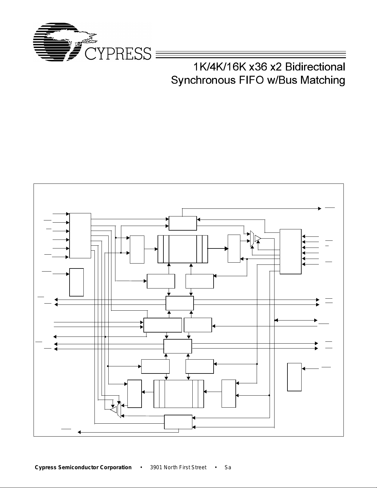
Logic Block Diagram
CY7C43642
CY7C43662
CY7C43682
... [ [ %LGLUHFWLRQDO
• Fully asynchronous and simultaneous rea d and writ e
operation permitted
• Mailbox bypass register for each FIFO
• Parallel Pr ogram m able Almost Full and Almost Empty
flags
• Retransmit function
• Standar d or FWFT mode user selectable
• 120-pin TQFP packaging
• Easily expandable in width and dept h
CLKA
CSA
W/RA
ENA
MBA
RT2
RST1
FFA/IRA
AFA
FS0
FS1
A
0–35
EFA/ORA
AEA
Port A
Control
Logic
FIFO1,
Mail1
Reset
Logic
Input
Register
Programmable
Flag Offset
Registers
Output
Register
Write
Pointer
Write
Pointer
Mail1
Register
1K/4K/16K
x36
Dual Ported
Memory
Status
Flag Logic
Status
Flag Logic
256/512/1K
4K/16K x36
Dual Ported
Memory
Read
Pointer
Timing
Mode
Read
Pointer
Input
Output
Register
MBF1
CLKB
Port B
Control
Register
Logic
FIFO2,
Mail2
Reset
Logic
CSB
W/RB
ENB
MBB
RT1
EFB/ORB
AEB
B
0–35
FWFT/STAN
FFB/IRB
AFB
RST2
Mail2
Register
MBF2
Cypress Semiconductor Corporation • 3901 North First Street • San Jose • CA 95134 • 408-943-2600
July 28, 2000
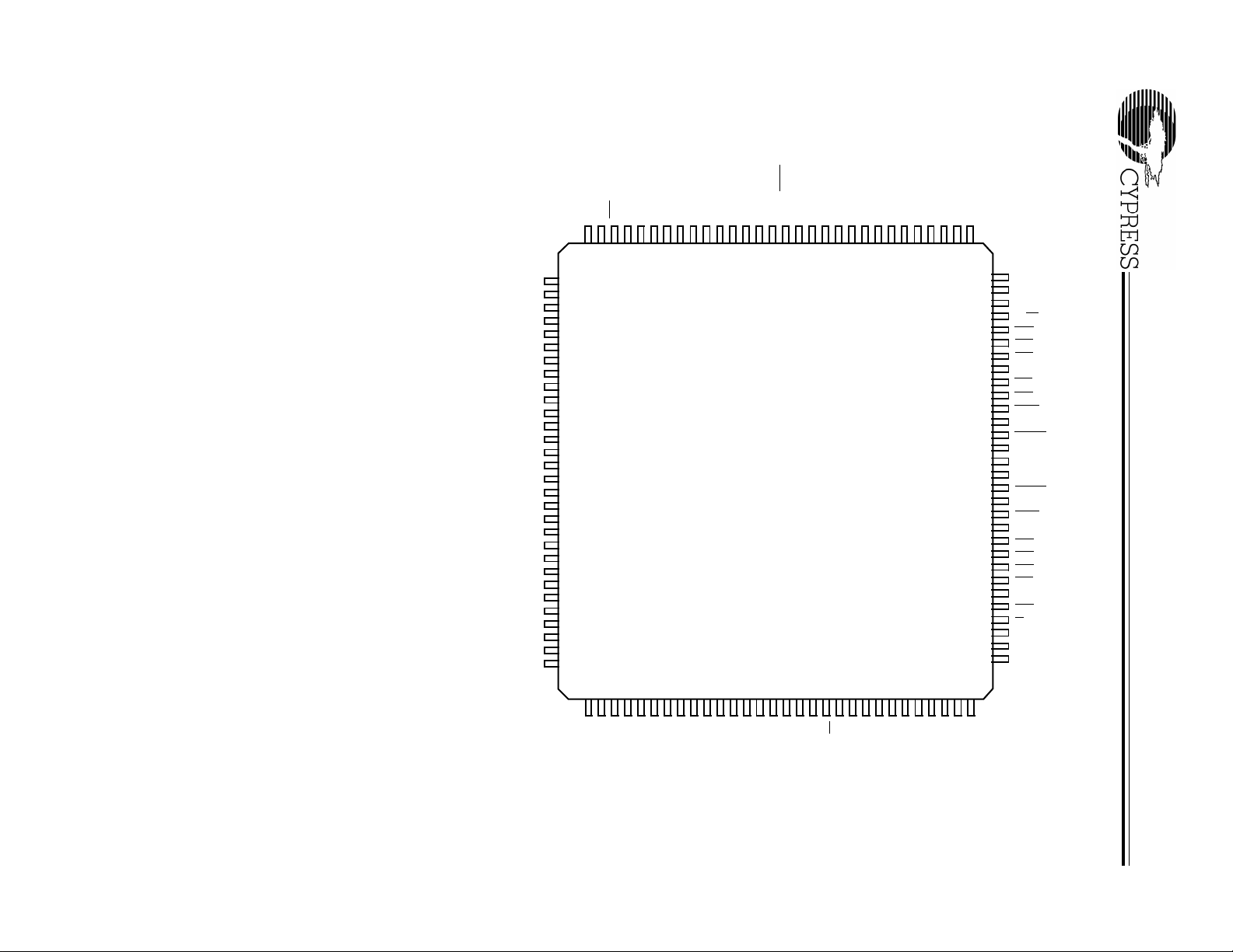
Pin Configuration
FWFT/STAN
RT2
A
A
A13A15A16A
14
12
27
28
29
30
31
GND
A
32
11
A
33
10
34
A
9
35
A
8
36
A
7
37
A
6
38
GND
A
39
5
40
A
4
41
A
3
42
V
CC
43
A
2
44
A
1
45
A
2
GND
GND
V
B
B
0
46
47
B
0
48
B
1
49
B
2
50
B
3
51
B
4
52
B
5
53
54
B
6
55
CC
56
B
7
57
B
8
58
B
9
59
10
60
11
64
63
62
61
GND
A18A19A20A
17
22
23
24
25
26
69
68
67
66
65
V
A23A24A25A26A
A
CC
21
22
12
13
14
15
16
17
18
19
20
21
CY7C43642
CY7C43662
CY7C43682
79
78
77
76
75
74
73
72
71
70
GND
A
A
27
28
29
11
82
81
80
V
A30A
A32A33A34A
CC
31
5
6
7
8910
86
85
84
83
35
1
234
120
GND
119
CLKA
118
ENA
117
W/RA
116
CSA
115
FFA/IRA
114
EFA/ORA
113
V
112
111
110
109
108
107
106
105
104
103
102
101
100
90
89
88
87
CC
AFA
AEA
MBF2
MBA
MRST1
Top View
FS0
GND
FS1
MRST2
MBB
TQFP
MBF1
V
CC
AEB
99
AFB
98
EFB/ORB
97
FFB/IRB
96
GND
95
CSB
94
W/RB
93
ENB
92
CLKB
91
V
CC
GND
B12B13B15V
B24B25RT1
B
B27B
26
28
B29B30B
31
GND
B32B33B34B
35
CY7C43682
CY7C43642
CY7C43662
GND
B
14
CC
B16B17GND
B18B19B20B21B
B
23
22
CY7C43642
CY7C43662
CY7C43682
Functional Description
The CY7C436X2 is a monolithic, high-speed, low-power,
CMOS Bidirectional Synchronous (clocked) FIFO memory
which supports clock fr equencies up to 133 MHz and has read
access times as fast as 6 ns. Two independent 1K/4K/16K x
36 dual-port SRAM FIFOs on board each chip buffer data in
opposite directions.
The CY7C436X2 is a synchronous (clocked) FIFO, meaning
each port employs a synchronous interface. All dat a transf ers
through a port are gated to the LOW-to-HIGH transition of a
port clock by enable signals. The clocks for each port are independent of one another and can be asynchronous or coincident. The enables for each port are arranged to provide a
simple bidi rectional i nterfac e between microproces sors and/or
buses with synchronous contro l.
Communicat ion betw een ea ch port may b ypa ss the FIF Os vi a
two mailbox registers. The mailbox registers’ width matches
the selected P o rt B bus width. Each mailbo x registe r has a flag
(MBF1
and MBF2) to signal when new mail has been stored.
Master Reset initializes the read and write pointers to the first
location of the memory array, and selects parallel flag programming, or one of the three possible default flag offset settings, 8 , 16, o r 64. Eac h FIFO has it s ow n indep endent M aster
Reset pin, RST1
The CY7C436X2 have two modes of operation: In the CY
Standard Mode, the first word writt en to an empty FIFO is deposited into the memory array. A read operation is required to
access that word (along with all other words residing in memory). In the First-Word Fall-Through Mode (FWFT), the first
word (36-bi t wide) written to an emp ty FIFO appe ars auto matically on the output s, no read operatio n required (nev ertheless,
accessing subsequent words does necessitate a formal read
request). The state of the FWFT
operation determines the mode in use.
and RST2.
/STAN pin during FIFO
Each FIFO has a combined Empty/Output Ready Flag (EFA
ORA and EFB
(FFA
/IRA and FFB/IRB). The EF and FF func tions are selected
in the CY Standard Mode. EF
is full or not. The IR and OR functions are sele cted in the First Word F all -Through Mode . IR indicates whet her or not the FIFO
has av ail able memory locations. OR shows whether the FIFO
has data availab le for reading or not. It marks the presence of
valid data on the outputs. (See f ootnote #17.)
Each FIFO has a programmable Al m ost Empty flag (AEA
AEB
) and a programmable Almost Full flag (AFA and AFB).
AEA
and AEB indic ate when a sele cted num ber of w ords written to FIFO memory achieve a predetermined “almost empty
state.” AFA
words written t o the m emory achieve a predet ermined “almost
full sta te.” (See footnote #34.)
IRA, IRB, AFA
writes data into its array. ORA, ORB, AEA
chronized to th e port clock that reads data from its array. Programmable offset for AEA
parallel usi ng P ort A. Three def ault off set settings are also pro vided. The AEA
locations from the empty boundary and AFA
threshold can be set at 8, 16, or 64 locations from the full
boundary. All these choices are m ade using the FS0 an d FS1
inputs during Master Reset.
Two or more devices may be used in parallel to create wider
data paths. If at any time the FIFO is not actively performing a
function, the chip will automatically power down. During the
power-down state, supply current consumption (I
minimum. Init iating a ny oper ati on (b y act iv ati ng con trol inputs )
will immediately take the device out of the power-do wn state.
The CY7C436X2 are characterized for operation from 0°C to
70°C commercial, and from –40°C to 85°C industrial. Input
ESD protection is gr eater than 2001V, and latch -up is pre vented by the use of guard rings.
/ORB) and a combined Full/Input Ready Flag
indicates whether the memory
and
and AFB indicate when a selected number of
, and AFB are synchroni zed to the port clock that
, and AEB are syn-
, AEB, AFA, and AFB are loaded in
and AEB threshold can be set at 8, 16, or 64
and AFB
) is at a
CC
/
Selectio n Gu ide
CY7C43642/62/82
Maximum Frequency (MHz) 133 100 66.7
Maximum Access Time (ns) 6 8 10
Minimum Cycle Time (ns) 7.5 10 15
Minimum Data or Enable Set-Up (ns) 3 4 5
Minimum Data or Enabl e Hold ( ns) 0 0 0
Maximum Flag Delay (ns) 6 8 8
Active Power Supply
Current (I
Density 1K x 36 4K x 36 16K x 3 6
Package 120 TQFP 120 TQFP 120 TQFP
CC1
) (mA)
Commercial 100 100 100
Industrial 100
CY7C43642 CY7C43662 CY7C43682
-7
CY7C43642/62/82
-10
CY7C43642/62/82
-15
3
CY7C43642
CY7C43662
CY7C43682
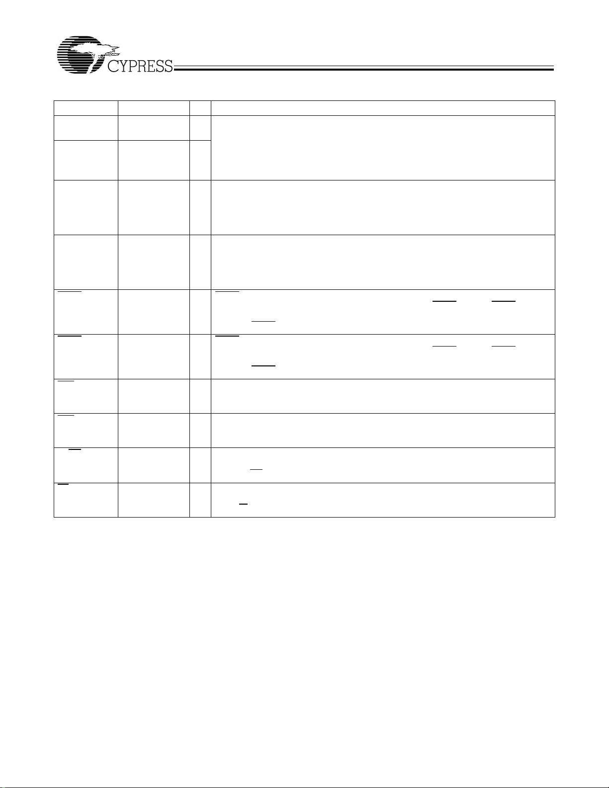
Pin Definitions
Signal Name Description I/O Function
A
0–35
AEA
AEB
AFA
AFB
B
0–35
/STAN B ig Endian/
FWFT
CLKA Port A Clock I CLKA is a co ntinuous clock t hat sy nchroniz es all data t ransf ers thr ough P ort A and can
CLKB Port B Clock I CLKB is a co ntinuous clock t hat sy nchroniz es all data t ransf ers thr ough P ort B and can
CSA
CSB
/ORA Port A Empty/
EFA
EFB
/ORB Port B Empty/
ENA Port A Enable I ENA must be HIGH to enab le a LOW -to-HIGH t ransi tion of CLKA to r ead or write dat a
ENB Port B Enable I ENB must be HIGH to enab le a LOW -to-HIGH t ransi tion of CLKB to r ead or write dat a
FFA
/IRA Port A Full/Input
/IRB Port B Full/Input
FFB
Port A Data I/O 36-bit bidirect ional data port for side A.
Port A Almost
Empty Flag
Port B Almost
Empty Flag
Port A Almost
Full Flag
Port B Almost
Full Flag
Port B Data I/O 36-bit bidirect ional data port for side B.
First-Word FallThrough Select
Port A Chip
Select
Port B Chip
Select
Output Ready
Flag
Output Ready
Flag
Ready Flag
Ready Flag
O Programmab le Almost Empt y flag sy nchronized to CLKA. It i s LOW when the nu mb er
of words in FIFO2 is less than or equal to the value in the Almost Empty A offset register,
X2. (See footnote #34 .)
O Programmab le Almost Empt y flag syn chronized t o CLKB. It is LOW when the number
of words in FIFO1 is less than or equal to the value in the Almost Empty B offset register,
X1. (See footnote #34 .)
O Programmab le Almost Full flag synchronized to CLKA. It is LOW when the number of
empty locations in FIFO1 is less than or equal to the value in the Almost Full A offset
register, Y1. (See f ootnote #34.)
O Programmab le Almost Full f lag synchronized to CLKB. It is LO W when the number of
empty locations in FIFO2 is less than or equal to the value in the Almost Full B offset
register, Y2. (See f ootnote #34.)
I During Master Reset. A HIGH on FWFT
First-Wor d Fall-Through m ode. Once the timing mode has been selected, the le vel on
FWFT
/STA N m ust be static throughout devic e operation.
be asynchronous or coincident to CLKB. FFA
synchronized to the LOW-t o-HIGH transition of CLKA.
be asynchronous or coincident to CLKA. FFB
synchronized to the LOW-to-HIGH transition of CLKB.
ICSA must be LOW to enable a LOW- to HIGH transition of CLKA to read or write on
Port A. The A
ICSB must be LOW to enable a LOW- to HIGH transition of CLKB to read or write on
Port B. The B
O This is a dual-function pin. In the CY Standard Mode, the EFA
indicates whether or not the FIFO2 memory is empty. In the FWFT mode, the ORA
function is selected. ORA indicates the presence of valid data on A
able for reading. EFA
(See footnot e #17.)
O This is a dual-funct ion pin. In the CY Standard Mode, the EFB
indicates whether or not the FIFO1 memory is empty. In the FWFT mode, the ORB
function is selected. ORB indicates the presence of valid data on B
able for reading. EFB
(See footnot e #17.)
on Port A.
on Port B.
O This is a dual-fun ction pin . In the CY Standar d Mode, the FFA function is selected . FF A
indicates whether or not t he FIFO1 me mory is full. In t he FWFT mode , the IRA function
is selected. IRA indicat es whether or not there is space av ailable f or writing to the FIFO1
memory. FFA
O This is a dual-function pin. In the CY Standard Mode, the FFB functio n is selected. FFB
indicates whether or not t he FIFO2 me mory is full. In t he FWFT mode , the IRB function
is selected. IRB indicat es whether or not there is space av ailable f or writing to the FIFO2
memory. FFB
outputs are in the high-im pedance state when CSA is HIGH.
0–35
outputs are in the high- impedance state when CSB is H IGH.
0–35
/ORA is synchronized to the LOW-to-HIGH tra nsition of CLKA.
/ORB is synchronized t o the LOW -t o-HIGH transition of CLKB.
/IRA is synchroniz ed to the LOW-to-HIGH transit ion of CLKA.
/IRB is synchronized to the LOW -to-HIGH transi tion of CLKB.
selects CY Standard mode, a LOW select s
/IRA, EFA/OR A, A FA, and AEA are all
/IRB, EFB /ORB, AFB, and AEB are all
function is selected. EFA
outputs, avail-
0–35
function is selected. EFB
outputs, avail-
0–35
4
CY7C43642
CY7C43662
CY7C43682
Pin Definitions
Signal Name Description I/O Function
FS1 Flag Offset
FS0 Flag Offset
MBA P ort A Ma i lbox
MBB P ort B Ma i lbox
MBF1
MBF2
RT1
RT2
W/RA
RB Port B Write/
W/
(continued)
Select 1
Select 0
Select
Select
Mail1 Register
Flag
Mail2 Register
Flag
Retransmit
FIFO1
Retransmit
FIFO2
Port A Write/
Read Select
Read Select
I The LO W-to-HI GH transition of a FIFO’s reset i nput la tches the va lues of FS0 and F S1.
If either FS0 or FS1 is HIGH when a reset input goes HIGH, one of the three preset
values (8, 16, or 64) is sel ected as the offset f or the FIFO’s Almost Full and Almost
I
Empty flags. If both FIFOs are reset simul taneously and both FS0 and FS1 are LOW
when RST1 and RST2 go HIGH, the first fo ur writes to FIFO1 Almost Empty offsets f or
both FIFOs.
I A HIGH level on M BA chooses a mail box register for a Port A read or write operation.
When a read operatio n is perf ormed on Port A, a HIGH le v el on MBA select s data from
the Mail2 register for output and a LOW level selects FIFO2 out put r egister data for
output. When a write oper ati on is p erf ormed on Port A, a HIGH lev el on MBA wi ll writ e
the data into Mail1 register while a LOW level will write the data into FIFO1.
I A HIGH level on M BB chooses a mail box register for a Port B read or write operation.
When a read operatio n is perf ormed on Port B, a HIGH lev el on MBB select s data from
the Mail1 register for output and a LOW level selects FIFO1 out put r egister data for
output. When a write oper ati on is per f ormed on Port B, a HIGH l ev e l on MBB wil l write
the data into Mail2 register while a LOW level will write the data into FIFO2.
OMBF1 is set LOW by a LOW-to-HI G H transition of CLKA that writes data to the Mail1
register. Writes to the Mail1 register are inhibited while MBF1
HIGH by a LOW -to-HIGH transition of CLKB when a Port B read is s elected and MBB
is HIGH. MBF1
OMBF2 is set LOW by a LOW-to-HI G H transition of CLKB that writes data to the Mail2
register. Writes to the Mail2 register are inhibited while MBF2
HIGH by a LOW -to-HIGH transition of CLKA when a Port A read is s elected and MBA
is HIGH. MBF2
I A LO W st robe on t his pi n will r etransm it the d ata on FIFO1. Th is is achie ved by bringing
the read point er back to loca tion zero . The user will still need to perform re ad operations
to retransmit the dat a. Retransmit func tion applies to CY standard mo de only.
I A LOW strobe on this pin will retr ansmit data on FIFO2. This is achiev ed by bringing
the read point er back to loca tion zero . The user will still need to perform re ad operations
to retransmit the dat a. Retransmit func tion applies to CY standard mo de only.
I A HIGH selects a write operat ion and a LOW selects a read oper ation on P ort A f or a
LOW- to-HI GH tra nsi tion of CLKA. The A
when W/RA
I A LOW selects a write operation and a HIGH selects a read oper ation on Port B for a
LOW- to-HIGH tra nsition of CLKB. The B
when W
is set HIGH following either a Master or Partial Reset of FIFO1.
is set HIGH following either a Master or Partial Reset of FIFO2.
0–35
is HIGH.
0–35
/RB is LOW.
is LOW. MBF1 is set
is LOW. MBF2 is set
outputs are in the HIGH impedance state
outputs ar e in t he HIGH impeda nce state
5

CY7C43642
CY7C43662
CY7C43682
Maximum Ratings
[1]
Static Discharge Voltage ............. .. ............ ............ ....>2001V
(per MIL-STD-883, Method 3015)
(Abov e which the useful life may be impaired. For user guidelines, not tested.)
Latch -U p Cu rre n t.............. .......... ......... .......... .......... . >200mA
Storage Temperature ....................................... −65°C to +150°C
Ambient Temperature with
Operating Range
Power Applied....................................................− 55°C to +125°C
Supply Voltage to Ground Pot ential..................−0.5V to +7.0V
DC Voltage Applied to Outp uts
in High Z State
DC Input Voltage
[2]
..........................................−0.5V to V
[2]
........................................−0.5V to V
CC
CC
+0.5V
+0.5V
Output C ur re n t in to O u tp u ts (LOW) ..... ......... .......... .....20 mA
Electrical Characteristics
Over the Operating Range
Parameter Description Te st Condi tions
V
V
V
V
I
IX
I
OZL
I
OZH
I
CC1
I
SB
OH
OL
IH
IL
[4]
[5]
Output HIGH Voltage VCC = 4.5V,
I
= −4.0 mA
OH
Output LOW Voltage VCC = 4.5V,
I
= 8.0 mA
OL
Input HIGH Voltage 2.0 V
Input LOW Voltage
Input Leakage Curren t V
Output OFF, High Z
Current
= Max. −10 +10 µA
CC
OE > VIH,
V
< VO< V
SS
Active Power Supply
Current
Average Standby
Current
Range
Ambient
Temperature
[3]
V
CC
Commercial 0°C to +70°C 5.0V ± 0.5V
Industrial
−40°C to +85°C
5.0V ± 0.5V
CY7C43642/62/82
2.4 V
0.5 V
CC
−0.5
−10
CC
0.8 V
+10
Com’l 100 mA
Ind 100 mA
Com’l 10 mA
Ind 10 mA
UnitMin. Max.
V
µA
[
Capacitance
]
Parameter Description Test Conditions Max. Unit
C
IN
C
OUT
Notes:
1. Stresses beyond those listed under “Absolute Maximum Ratings” may cause permanent damage to the device. These are stress ratings only and functional
operation of the device at these or any other conditions beyond those indicated under “recommended operating conditions” is not implied. Exposure to absolutemaximum-rated conditions for extended periods may affect device reliability.
2. The input and output voltage ratings may be exceeded provided the input and output current ratings are observed.
3. Operating V
4. Input signals switch from 0V to 3V with a rise/fall time of less than 3 ns, clocks and clock enables switch at 20 MHz, while data inputs switch at 10 MHz. Outputs
are unloaded.
5. All inputs = V
6. Tested initially and after any design or process changes that may affect these parameters.
Range for -7 speed is 5.0V ± 0.25V.
CC
– 0.2V, except RCLK and WCLK (which are at frequency = 0 MHz). All outputs are unloaded.
CC
Input Capacit ance TA = 25°C, f = 1 MHz,
V
= 3.3V
Output Capacitance 8 pF
CC
4 pF
6
AC Test Loads and Waveforms (-1 0 & -15)
R1=1.1k
5V
OUTPUT
INCLUDING
C
=30 pF
L
JIG AND
SCOPE
Ω
R2=680
Ω
AC Test Loads and Waveforms (-7)
3.0V
GND
≤
3ns
ALL INPUT PULSES
90%
10%
CY7C43642
CY7C43662
CY7C43682
90%
10%
3
ns
≤
50Ω
I/O
Switching Characteristics
=
Ω
Over the Operating Range
Parameter Description
f
S
t
CLK
t
CLKH
t
CLKL
t
DS
t
ENS
t
RSTS
t
FSS
t
SDS
t
SENS
t
FWS
t
DH
Clock Frequency, CLKA or CLKB 133 100 67 MHz
Clock Cycle Time, CLKA or CLKB 7.5 10 15 ns
Pulse Duration, CLKA or CLKB HIGH 3.5 4 6 ns
Pulse Duration, CLKA or CLKB LO W 3.5 4 6 ns
Set-Up Time, A
CLKB↑
before CLKA ↑ and B
0–35
Set-Up Time, CSA, W/RA, ENA, and MBA before
CLKA↑; CSB
Set-Up Time, RST1 or RST2 LOW before CLKA↑ or
CLKB↑
, W/RB, ENB, and MBB bef or e CLK B↑
[7]
Set-Up Time, FS0 an d FS1 befor e RST1 and RST2
HIGH
Set-U p Tim e, F S0 b efor e CLK A ↑ 3 4 5 ns
Set-U p Tim e, F S1 b efor e CLK A ↑ 3 4 5 ns
Set-Up Time, FWFT bef ore CLKA↑ 0 0 0 ns
Hold Time, A
after CLKA↑ and B
0–35
CLKB↑
t
ENH
t
RSTH
Hold Time, CSA, W/RA, ENA, and MBA after
CLKA↑; CS B
Hold Time, RST1 or RST2, LOW after CLKA↑ or
CLKB↑
, W/RB, ENB, and MBB after CLKB↑
[7]
VCC/2
0–35
0–35
after
before
ALL INPUT PULSES
3.0V
GND
3ns
≤
CY7C43642/
62/82
-7
90%
10%
CY7C43642/
62/82
-10
90%
10%
≤
CY7C43642/
3
ns
62/82
-15
3 4 5 ns
3 4 5 ns
2.5 4 5 ns
6 7 7.5 ns
0 0 0 ns
0 0 0 ns
1 2 4 ns
UnitMin. Max. Min. Max. Min. Max.
7
CY7C43642
CY7C43662
CY7C43682
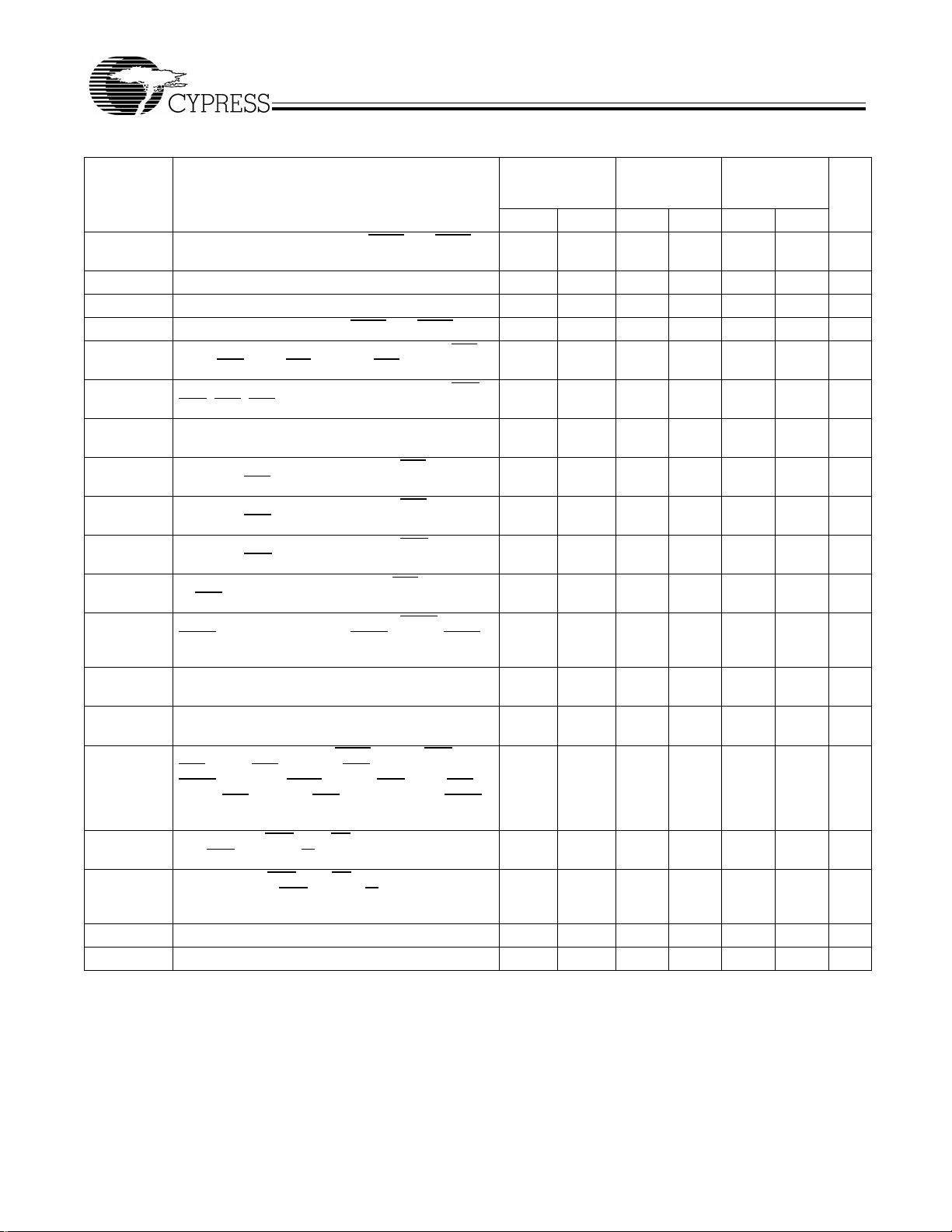
Switching Characteristics
Over the Operating Range (continued)
CY7C43642/
62/82
-7
CY7C43642/
62/82
-10
CY7C43642/
62/82
-15
Parameter Description
t
FSH
Hold Time, FS0 and FS1 after RST1 and RST2
1 1 2 ns
HIGH
t
SDH
t
SENH
t
SPH
t
SKEW1
t
SKEW2
t
A
t
WFF
t
REF
t
PAE
t
PAF
t
PMF
Hold Time, FS0 after CLKA↑ 0 0 0 ns
Hold Time, FS1 after CLKA↑ 0 0 0 ns
Hold Time, FS1 HIGH after RST1 and RST2 HIGH 0 1 2 ns
[7]
Skew Ti m e betwe en CLK A ↑ and CLKB↑ for EFA/
ORA, EFB
[7]
Skew Ti m e betwe en CLK A ↑ and CLKB↑ for AEA,
AEB
Access Time, CLKA↑ to A
B
0–35
/ORB, FFA/IRA, and F F B/IRB
, AF A , AFB
0–35
and CLKB↑ to
Propagation Delay Time, CLKA↑ to FFA/IRA and
CLKB↑ to FFB
/IRB
Propagation Delay Time, CLKA↑ to EFA/ORA and
CLKB↑ to EFB
/ORB
Propagation Delay Time, CLKA↑ to AEA and
5 5 7.5 ns
7 8 12 ns
1 6 1 8 3 10 ns
1 6 1 8 2 8 ns
1 6 1 8 1 8 ns
1 6 1 8 1 8 ns
CLKB↑ to AEB
Propagation Dela y Time, CLKA↑ to AF A and CLKB↑
1 6 1 8 1 8 ns
to AFB
Propagation Delay Time, CLKA↑ to MBF1 LOW or
MBF2
HIGH and CLKB↑ to MBF2 LOW or MBF1
0 6 0 8 0 12 ns
HIGH
t
PMR
t
MDV
t
RSF
Propagation Delay Time, CLKA↑ to B
CLKB↑ to A
0–35
[9]
Propagation Delay Time, MBA to A
MBB to B
0–35
valid
Propagation De lay Ti me, RST1 LOW to AEB LOW,
AFA
HIGH, FFA/IRA Low, EFB/ORB LOW, and
MBF1
HIGH and RST2 LOW to AEA LOW, AFB
HIGH, FFB
/IRB Low, EFA/ORA LOW, and MBF2
0–35
valid and
0–35
[8]
and
1 7 2 11 3 12 ns
1 6 2 9 3 11 ns
1 6 1 10 1 15 ns
HIGH
t
EN
t
DIS
t
PRT
t
RTR
Notes:
7. Ske w time is not a timing constraint for proper device operation and is only included to illustrate the timing relationship between the CLKA cycle and the CLKB
cycle.
8. Writing data to the Mail1 register when the B
9. Writing data to the Mail2 register when the A
10. Requirement to count the clock edge as one of at least four needed to reset a FIFO.
Enable Time, CSA or W/RA LOW to A
and CSB
LOW and W/RB HIGH to B
Disable Time, CSA or W/RA HIGH to A
Impedance and CSB
HIGH or W/RB LOW to B
at High Impedance
0–35
0–35
0–35
Active
Active
at High
0–35
1 6 2 8 2 10 ns
1 5 1 6 1 8 ns
Retransmit Pulse Width 60 60 60 ns
Retransmit Recovery Time 90 90 90 ns
outputs are active and MBB is HIGH.
0–35
outputs are active and MBA is HIGH.
0–35
UnitMin. Max. Min. Max. Min. Max.
8
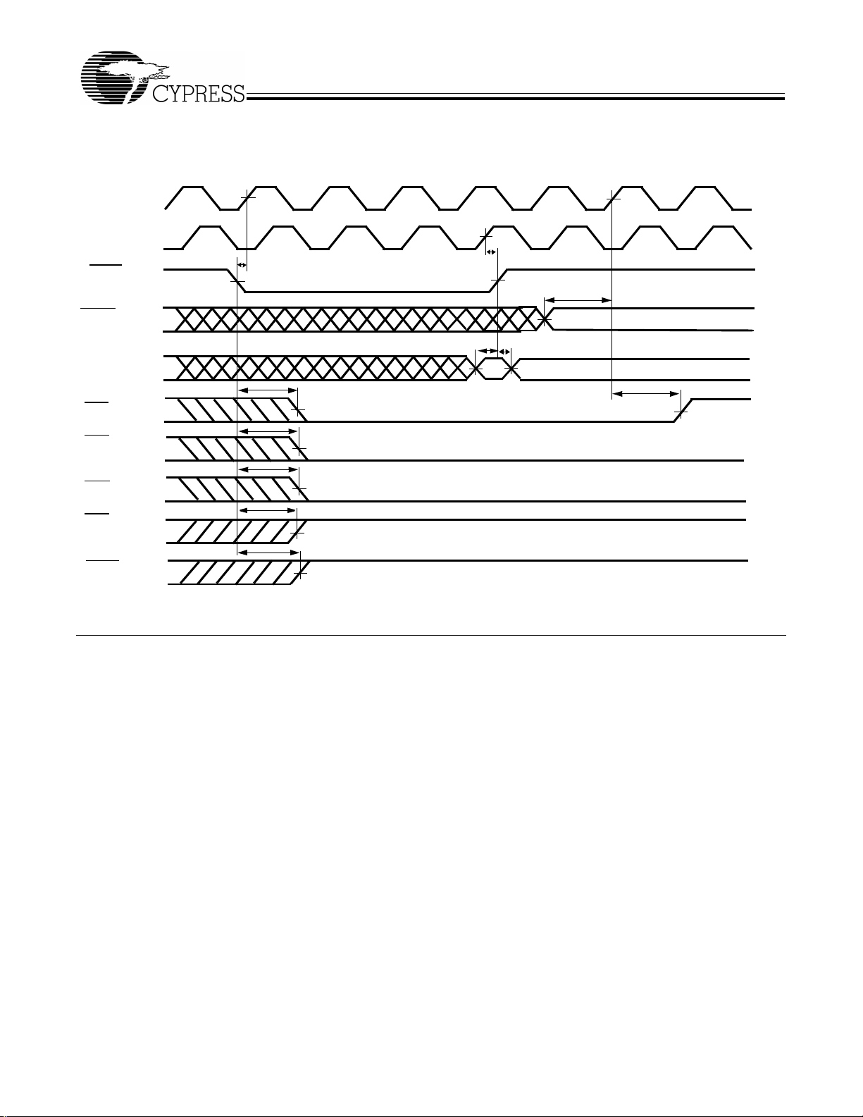
Switching Waveforms
CY7C43642
CY7C43662
CY7C43682
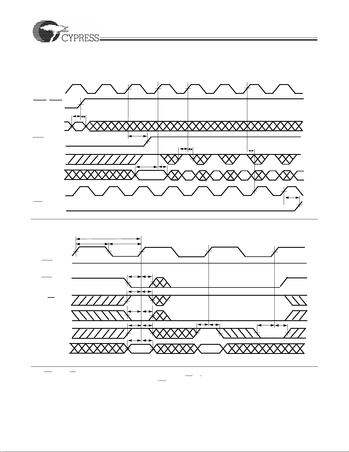
FIFO1 Reset Loading X1 and Y1 with a Preset Value of Eight
CLKA
CLKB
t
RST1
RSTS
FWFT/STAN
FS1, FS0
t
RSF
FFA
/IRA
t
EFB
/ORB
RSF
t
RSF
AEB
t
RSF
AFA
t
RSF
MBF1
[11]
t
FSS
t
RSTH
t
FSH
t
FWS
t
WFF
Note:
11. Reset is performed in the same manner for FIFO2 to load X2 and Y2 with a preset value.
9
CY7C43642
CY7C43662
CY7C43682
Switching Waveforms
Programming of the Almost- Full Flag and Almost-Empty Flag Offset Values after Reset
(CY Standard and FWFT Modes)
(continued)
[12]
CLKA
RST1
, RST2
t
t
FSH
FSS
FS1, FS0
t
FFA/
IRA
WFF
t
ENStENH
ENA
t
A
DS
0−35
AFA Offset (Y1)
t
DH
AEB Offset (X1)
AFB Offset (Y2)
AEA Offset (X2)
CLKB
FFB
/IRB
t
SKEW1
[13]
First Word to FIFO1
t
WFF
Port A Write Cycle Timing for FIFO1 (CY Standard and FWFT Modes)
t
CLK
t
CLKH
t
CLKL
CLKA
FFA/
IRA
HIGH
t
ENS
t
ENH
CSA
t
W/RA
ENS
t
ENStENH
t
ENH
MBA
ENA
A
0–35
Notes:
12. CSA
13. t
14. Written to FIFO1.
=LOW, W/RA=HIGH, MBA=LOW. It is not necessary to program offset register on consecutive clock cycles.
is the minimum time between the rising CLKA edge and a rising CLKB for FFB/IRB to transition HIGH in the next cycle. If the time between the rising
SKEW1
edge of CLKA and rising edge of CLKB is less than t
t
ENS
t
DS
W1
SKEW1
t
ENH
t
DH
[14]
, then FFB/IRB may transition HIGH one cycle later than shown.
t
ENS
W2
[14]
t
ENH
t
ENS
t
ENH
10
 Loading...