

Cypress Semiconductor CY7C43686AV-7AC, CY7C43686AV-15AC, CY7C43686AV-10AC, CY7C43646AV-7AC, CY7C43646AV-15AC Datasheet
...
V
CY7C43646AV
PRELIMINARY
3.3 V 1K/4K/16K x36/x18x2 Tri Bus FIFO
Features
• 3.3V high-speed, low-power, first-in first-out (FIFO)
memories w/ three in dependent ports (one bidirectional
x36, and two unidir ectional x18)
• 1K x36/x18x2 (CY7C43646AV)
• 4K x36/x18x2 (CY7C43666AV)
• 16K x36/x18x2 ( CY7C43686AV)
• 0.25-micron CMOS for optimum speed/pow er
• High-speed 133- MHz operat ion (7.5- ns read/wri te cy cle
times)
• Low po w er
= 60 mA
—I
CC
= 12 mA
—I
SB
• Fully asynchronous and simultaneous read and write
operation permitted
• Mailbox bypass register for each FIFO
• Parallel and Serial Programmable Almost Full and
Almost Empty flags
• Retransmit function
• Standard or FW FT mode user sel ectable
• Partial Reset
• Big or Little Endian f ormat for word or byte bus sizes
• 128-pin TQFP packaging
• 3.3V pin-compatible, feature enhanced, density upgrade to IDT723626/36/46 family
• Easily expandable in width and depth
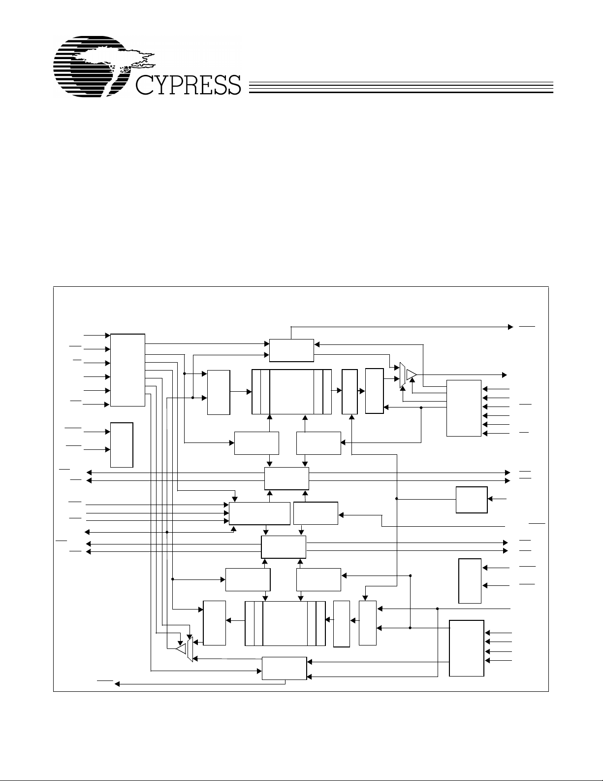
CY7C43666AV/CY7C43686AV
Logic Block Diagram
CLKA
CSA
W/RA
ENA
MBA
RT2
MRS1
PRS1
FFA/IRA
AFA
SPM
FS0/SD
FS1/SEN
A
0–35
EFA/ORA
AEA
MBF2
Por t A
Control
Logic
FIFO1,
Mail1
Reset
Logic
Input
Register
Programmable
Flag Offset
Registers
Output
Register
Write
Pointer
Read
Pointer
Mail1
Register
1K/4K/16K
x36
Dual Ported
Memory
Status
Flag Logic
Status
Flag Logic
1K/4K/16K
x36
Dual Ported
Memory
Mail2
Register
Read
Pointer
Timing
Mode
Write
Pointer
Input
Bus Matching
MBF1
B
0–17
CLKB
Output
Output
Register
Bus Matching
Input
Register
Port B
Control
Logic
Common
Port Logic
(B and C)
FIFO2,
Mail2
Reset
Logic
Port C
Control
Logic
RENB
CSB
SIZEB
MBB
RTI
EFB/ORB
AEB
BE
BE/FWFT
FFC/IRC
AFC
MRS2
PRS2
C
0–17
CLKC
WENC
SIZEC
MBC
Cypress Semiconductor Corporation
• 3901 North First Street • San Jose • CA 95134 • 408-943-2600
September 3, 1999
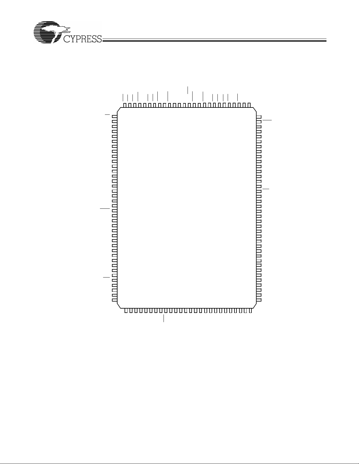
Pin Configuration
W/RA
ENA
CLKA
GND
A
A
A
A
V
A
A
GND
A
A
A
A
A
A
A
BE/FWFT
GND
A
V
A
A
A
A
GND
A
A
A
A
A
RT2
A
GND
A
A
CY7C43646AV
PRELIMINARY
TQFP
Top View
MBF2
AEA
AFA
VCCPRS1
EFA/ORA
FFA/IRA
CSA
128
127
126
125
124
123
1
2
3
122
4
5
35
6
34
33
7
32
8
9
CC
10
31
11
30
12
29
13
14
28
15
27
26
16
25
17
24
18
19
23
20
21
22
22
CC
23
21
24
20
25
19
26
18
27
28
17
29
16
30
15
31
14
32
13
33
34
12
35
36
11
37
10
38
39404142434445464748495051525354555657585960616263
5
6A7A8A9
A
GND
FS0/SD
FS1/SEN
GND
CLKC
MRS1
MBA
121
120
119
118
117
116
115
CY7C43646AV
CY7C43666AV
CY7C43686AV
2
0A1
A
A
A3A4A
CC
V
SPM
GND
CY7C43666AV/CY7C43686AV
GND
FFC/IRC
MRS2
114
B
AFC
AEB
VCCMBF1
MBB
113
112
111
110
109
0
5B4B3B2B1
B
EFB/ORB
108
CSB
RENB
WENC
107
106
105
104
103
102
CLKB
101
PRS2
V
100
CC
99
C
17
98
C
16
97
C
15
96
C
14
GND
95
MBC
94
93
C
13
92
C
12
91
C
11
90
C
10
89
C
9
88
C
8
RT1
87
86
C
7
C
85
6
SIZEB
84
83
GND
82
C
5
81
C
4
80
C
3
C
79
2
C
78
1
77
C
0
76
GND
B
75
17
74
B
16
SIZEC
73
V
72
CC
B
71
15
B
14
70
B
69
13
B
68
12
GND
67
B
66
11
B
65
10
64
7
6
B
GND
B9B8B
CC
V
2
PRELIMINARY
CY7C43646AV
CY7C43666AV/CY7C43686AV
Functional Description
The CY7C436X6AV is a monolithic, high-speed, low-power,
CMOS Bidirectional Synchronous (clocked) FIFO memory
which supports cloc k freque ncies up to 133 M Hz an d h as read
access times as fast as 6 ns. Two independent
256/512/1K/4K/16K x 36 dual-port SRAM FIFOs on board
each chip b uf fe r d ata i n opposi te di rec tions . FI FO data o n Port
B can be input and output in 36-bit, 18-b it, or 9-bit format s with
a choice of Big or Little Endi an configurations.
The CY7C436X6AV is a synchronous (clocked) FIFO, meaning each port emplo ys a sync hron ous int erf ace . All data t ransfers th rough a port are gate d to the LO W - to-HI GH trans iti on of
a port clock by enable signals. The clocks for each port are
independent of one another and can be asynchronous or coincident. The enables for each port are arranged to provide a
simple bidi rectional i nterfac e between microproces sors and/or
buses with synchronous control.
Communication b etw een each port ma y b ypas s the FIF Os via
two mailbox registers. The mailbox registers’ width matches
the selected P ort B bus width. Each mailbo x register has a f lag
(MBF1
and MBF2) to signal when new mail has been stored.
T w o kinds of reset are a vailab le on th e CY7C436X6A V : Master
Reset and Partial Reset . Master Rese t init ializ es t he read and
write pointers to the fi rst location of the memory array, configures the FIFO for Big or Little Endian byte arrangement and
selects serial flag programming, parallel flag programming, or
one of the three possible defaul t flag offset settings, 8, 16, or
64. Each FIFO has its own independent Master Reset pin,
MRS1
and MRS2.
Partial Reset also sets the read and write pointers to the first
location of the memory. Unlike Master Reset, any settings existing prior to P artial Reset ( i.e., progr amming meth od and partial flag default offsets) are retained. Par tial Reset is useful
since it permits fl ushing of the FI FO memory witho ut chang in g
any configuration settings. Each FIFO has its own independent Partial Reset pin, PRS1
The CY7C436X6AV have two modes of operation: In the CY
Standard Mode, the first word written to an em pty FIFO is deposited into the memory array. A read operation is requi red to
access that word (along with all other words residing in memory). In the Fi rst-Word Fall-Through Mode (FWFT ), the fi rst
long-word (3 6-bit wide) written to an empty FIFO appears au-
and PRS2.
tomatically on the out puts, no read operation required (nevertheless, accessing subsequent words does necessitate a formal read request). The state of the FWFT
FIFO operation determines the mode in use.
Each FIFO has a combined Empty/Output Ready Flag
(EFA
/ORA and EFB/ORB) and a combined Full/Input Ready
Flag (FFA
selected in the CY Standard Mode. EF
memory is full or not. The IR and OR funct ions are se lected in
the First Word Fal l Throu gh Mode. IR indic ates wheth er or not
the FIFO has available memory locations. OR shows whether
the FIFO has data available for reading or not. It marks the
presence of val id data on the outputs.
Each FIFO has a programmable Almost Empty flag (AEA
AEB
AEA
ten to FIFO memory achieve a predetermined “almost empty
state.” AFA
words written t o the m emory achi ev e a predet ermined “almost
full sta te.”
IRA, IRC, AFA
that writes data into its array. ORA, ORB, AEA
synchronized to the port clock that reads data from its array.
Programmable offset for AEA
in parallel using Port A or in serial via the SD input. Three
default offset settings are also provided. The AEA
threshold can be set at 8, 16, or 64 locations from the empty
boundary and AFA
64 locations from the full boundary. All these ch oices are made
using the FS0 and FS1 inputs during Master Reset.
Two or more devices may be used in parallel to create wider
data paths. Such a width expansion requires no additio nal external components.
If at any time the FIFO is not actively performing a function,
the chip will automatically power down. During the Power
Down state, supply cur rent cons umption (I
Initiating an y oper ation ( by ac tiv at ing c ontrol inp uts) will imme diately take the device out of the Power Down state.
The CY7C436X6AV are characterized for operation from 0
to 70°C. I nput ESD prot ection is g reater t han 2001V, and la tchup is prevented by the use of guard rings.
/IRA and FFC/IRC). The EF and FF functions are
) and a programmable Almost Full flag (AFA and AFC).
and AEB indicate when a selected number of words writ-
and AFC indicate when a selected number of
, and AFC are synchronized to the port clock
, AEB, AF A, and AF C are loa ded
and AFC threshold can be set at 8, 16, or
/STAN pin during
indicates whether the
and
, and AEB are
and AEB
) is at a minimum.
CC
°
C
Selection Guide
7C43646/66/86AV-7 7C43646/66/86AV-10 7C43646/66/86AV-15
Maximum Frequency (MHz) 133 100 66.7
Maximum Access Time (ns) 6 8 10
Minimum Cycle Time (ns) 7.5 10 15
Minimum Data or Enable Set-Up (ns) 3 4 5
Minimum Data or Enable Hold (ns) 0 0 0
Maximum Flag Delay (ns) 6 8 10
Active Power Supply
Current (I
Density 1K x 36/x18x2 4K x 36/18x2 16K x 36/x18x2
Package 128 TQFP 128 TQFP 128 TQFP
CC1
) (mA)
Commercial 60 60 60
Industrial 60
7C43646AV 7C43666AV 7C43686AV
3

CY7C43646AV
PRELIMINARY
Pin Definitions
Signal Name Description I/O Function
A
0–35
AEA
AEB
AFA
AFC
B
0–17
BE/FWFT
C
0–17
CLKA Port A Clock I CLKA is a c ontinuous clock t hat synchr onizes all data tr ansfer s through P ort A and can
CLKB Port B Clock I CLKB is a c ontinuous clock t hat synchr onizes all data tr ansfer s through P ort B and can
CLKC P ort C Clock I CLKC is a contin uous cloc k that synchroniz es all data tr ansfe rs throu gh P ort C and can
CSA
CSB
EFA
/ORA Port A Empty/
/ORB Port B Empty/
EFB
ENA Port A Enable I ENA must be HIGH to enable a L O W -to- HIGH tra nsition of CLKA to rea d or write dat a
ENB Port B Enable I ENB must be HIGH to enable a L O W -to- HIGH tra nsition of CLKB to rea d or write dat a
Port A Data I/O 36-bit bidirectional data port for side A.
Port A Almost
Empty Flag
Port B Almost
Empty Flag
Port A Almost
Full Flag
Port C Almost
Full Flag
Port B Data O 18-bit output data port for port B.
Big Endi-
an/First-Word
Fall-Through
Select
Port B Data I 18-bit input data port for port C.
Port A Chip
Select
Port B Chip
Select
Output Ready
Flag
Output Ready
Flag
O Programmab le Almost Empty flag sy nchroni z ed to CLKA. It is LO W when the nu mber
of words in FIFO2 is less t han or equa l to the val ue in the Alm ost Empty A of fset register ,
X2.
O Programmab le Almost Empty flag sync hro nize d to CLKB. It is LOW when the nu mber
of words in FIFO1 is less t han or equa l to the val ue in the Alm ost Empty B of fset register ,
X1.
O Programmable Almost Full flag synchroniz ed to CLKA. It is LOW when the n umber of
empty locations in FIFO1 is less than or equal to the value in the Almost Full A offset
register, Y1.
O Programmab le Almost Ful l flag synchron ized to CLKC. It is LOW when the number of
empty locations in FIFO2 is less than or equal to the value in the Almost Full B offset
register, Y2.
I This is a dual-purpose pin. During Maste r Reset, a HIGH on BE will selec t Big Endian
operation. In thi s case, depe nding on the bus size, the most signi ficant byt e or word on
Port A is read fr om Port B first (A- to- B data flow) or written to Port C first ( C-to-A data
flow). A LO W on BE will select Little Endia n operati on. In this case , the lea st significant
byte or word on Port A is read from Port B first (for A-to-B data flow) or written to Port
C first (C-to-A data flow). After Master Reset, this pin selects the timing mod e. A HIGH
on FWFT
Once the timing mode has be en selecte d, the le ve l on FWFT
device operation.
be asynchronous or coincident to CLKB. FFA
synchronized t o the LOW-to-HIGH transition of CLKA.
be asynchronous or coincident to CLKA. EFB
the LOW-to-HIGH transition of CLKB.
be asynchronous or coinciden t to CLKA. FFC
LOW-t o-HIGH transition of CLKC.
ICSA must be LOW to enable a LOW-to HIGH trans it ion of CLKA to read or write on
Port A. The A
ICSB must be LOW to enable a LOW-to HIGH trans it ion of CLKB to read or write on
Port B. The B
O This is a dual -functi on pin. In the CY S tandard Mode , the EF A f unction is selected. EF A
indicates whether or not the FIFO2 memo ry is empty. In the FWFT mode, the ORA
function is selected. ORA indicates the presence of valid data on A
able for reading. EFA
O This is a dual-funct ion pin. In the CY Standard Mode, the EFB funct ion is selected. EFB
indicates whether or not the FIFO1 memo ry is empty. In the FWFT mode, the ORB
function is selected. ORB indicates the presence of valid data on B
able for reading. EFB
on Port A.
on Port B.
selects CY Standard Mode , a LOW selects First-Word Fall-Through Mode.
outputs are in the high-impedance state when CSA is HIGH.
0–35
outputs are in the high- impedance state when CSB is HIGH.
0–17
/ORA is synchronized to t he LOW-to-HIGH transition of CLKA.
/ORB is synchronized to t he LOW-to-HIGH transition of CLKB.
CY7C43666AV/CY7C43686AV
must be stati c through out
/IRA, E FA/ORA, AFA, and AEA are all
/ORB and AEB are all synchronized to
/IRC and AFC are all synchr onized t o the
outputs, avail-
0–35
outputs, avail-
0–17
4
PRELIMINARY
CY7C43646AV
CY7C43666AV/CY7C43686AV
Pin Definitions
Signal Name Description I/O Function
FFA/IRA Port A Full/Input
/IRC Port C Full/I nput
FFC
FS1/SEN
FS0/SD Flag Offset
MBA Port A Mailbox
MBB Port B Mailbox
MBC Port C Mailbox
MBF1
MBF2
MRS1
MRS2
PRS1
PRS2
(continued)
Ready Flag
Ready Flag
Flag Offset
Select 1/Serial
Enable
Select 0/Serial
Data
Select
Select
Select
Mail1 Register
Flag
Mail2 Register
Flag
FIFO1 Master
Reset
FIFO2 Master
Reset
FIFO1 Partial
Reset
FIFO2 Partial
Reset
O This is a dual- function pi n. In the CY St andard Mode, the FFA function is s elected. FF A
indicates whether or not t he FIFO1 memory is full. In the FWFT mode , the IRA function
is selected. IRA indicat es whether or not there is space av ailable fo r writing to the FIFO1
memory. FFA
O This is a dual-funct ion pin. In the CY Standard Mode , the FFC funct ion is selected. FFC
indicates whether or not the FIFO2 mem ory is full. In the FWFT mode, t he IRC fun ction
is selected. IRC indicat es whether or not there is space a vailable f or writing to the FIFO2
memory. FFC
I FS1/SEN and FS0/SD are dual-purpose inputs used for flag offset register program-
ming. During Master Reset , FS1/ SEN
offset program ming method. Three offs et register prog ramming methods are a vailab le:
automatically load one of three preset v alues (8, 16, or 64), par allel load from Port A,
I
and serial load. When serial load is selected for flag off set register programming,
FS1/SEN
When FS1/SEN
the X and Y registers. The nu mber of bit writes requir ed to progr am the offset regis ters
is 40 for the CY7C43646AV, 48 for the CY7C43666AV, and 56 for the CY7C4368 6AV.
The first bit write stores the Y-register MSB and the last bit write stores the X-re gister
LSB.
I A HIGH lev el on MBA chooses a mailbox register for a Port A read or write operation.
When the A
register for output and a LOW level selects FIFO2 output register data f or output.
I A HIGH lev el on MBB chooses a mailbox register for a Port B read or write operation.
When the B
register for output and a LOW level selects FIFO1 output register data f or output.
I A HIGH lev el on MBC choose s a mailbox r egister for a Po rt C r ead or write operation.
When t he C
register for output and a LOW level selects FIFO1 output register data f or output.
OMBF1 is set LOW by a LOW-to-HIGH transition of CLKA that writes data to the Mail1
register. Writes to the Mail1 regis ter are inhibited while MBF1
HIGH by a LOW- to-HI GH transiti on of CLKB when a Po rt B read is selected and MBB
is HIGH. MBF1
OMBF2 is set LOW by a LOW-to-HIGH transition of CLKB that writes data to the Mail2
register. Writes to the Mail2 regis ter are inhibited while MBF2
HIGH by a LOW- to-HI GH transiti on of CLKA when a Po rt A read is selected and MBA
is HIGH. MBF2
I A LOW on this pin initializes the FIFO1 read and write pointers to the first location of
memory and sets the P ort B output register to a ll zeroes. A LOW puls e on MRS1
the programmi ng method (serial or parallel ) and one of th ree programmab le flag def ault
offsets f or FIFO1. It al so confi gures Port B for bus si ze and endi an arra ngement . Fou r
LOW-t o-HIGH transitions of CLKA and four LOW -t o-HIGH transitions of CLKB must
occur while MRS1
I A LOW on this pin initializes the FIFO2 read and write pointers to the first location of
memory and sets the P ort A output register to a ll zeroes. A LOW puls e on MRS2
one of three program ma ble flag default off sets for FIFO2. F our LOW-to-HIGH transitions of CLKA and four LOW-to-HIGH transitions of CLKB must occur while M RS2
LOW.
I A LOW on this pin initializes the FIFO1 read and write pointers to the first location of
memory and sets the Port B output register to all zeroes. During P artial Reset, the
currently selected bus size, e ndian arrangement, programming method (serial or parallel), and progr am m able flag settings are all retained.
I A LOW on this pin initializes the FIFO2 read and write pointers to the first location of
memory and sets the Port A output register to all zeroes. During P artial Reset, the
currently selected bus size, e ndian arrangement, programming method (serial or parallel), and progr am m able flag settings are all retained.
/IRA is syn ch r on i ze d to th e L OW-to-H IG H tra n s iti o n o f CLK A .
/IRC is syn ch r o ni zed to th e LOW-to-H IGH tra n s ition of CLKB .
and FS0/SD , toget her with SPM, sel ect the f lag
is used as an enable synchronou s to the LOW -to-HIGH transition of CLKA.
is LOW, a rising edge on CLKA loads the bit present on FS0/SD into
outputs are active, a HIGH lev el on MBA selects data from the Mail2
0–35
outputs are active, a HIGH lev el on MBB selects data from the Mail1
0–17
outputs are active, a HIGH level on MBC s elects data from the M ail1
0–17
is set HIGH following either a Master or P artial Reset of FIFO1.
is set HIGH following either a Master or P artial Reset of FIFO2.
is LOW.
is LOW. MBF1 is se t
is LOW. MBF2 is se t
selects
selects
is
5
PRELIMINARY
CY7C43646AV
CY7C43666AV/CY7C43686AV
Pin Definitions
(continued)
Signal Name Description I/O Function
RENB Port B Read
Enable
RT1
FIFO1
Retransmit
RT2
FIFO2
Retransmit
I RENB must be HIGH to enable a LOW-to-HIGH transition of CLKB to read data on
Port B.
I A LOW strobe on this pin will retransmit data on FIFO1 from the loc ati on of the write
pointer at the last P artial or Master reset.
I A LOW strobe on this pin will retransmit data on FIFO2 from the loc ati on of the write
pointer at the last P artial or Master reset.
SIZEB Bus Size Select I A HIGH on this pin when BM is HIGH selects byte bus (9-bit) size on Port B. A LO W
on this pin when BM is HIGH sele cts word (18-bit) bus size. SIZE works wit h BM and
BE to select the bus size and endian arrangement for Port B. The level of SIZE must
be static throughout device operation.
SIZEC Bus Size Select I A HIGH on this pin when BM is HIGH selects byt e bus (9-bit) size on Port B. A LOW
on this pin when BM is HIGH sele cts word (18-bit) bus size. SIZE works wit h BM and
BE to select the bus size and endian arrangement for Port B. The level of SIZE must
be static throughout device operation.
SPM
W/RA
WENC Port C Write
Maximum Ratings
(Abov e which the useful life may be impaired. For user guidelines, not tested.)
Storage Temperature .......................................−65°C to +150°C
Ambient Temperature with
Po wer Applied....................................................−55°C to +125°C
Supply Voltage to Ground Potential..................−0.5V to +7.0V
DC Voltage Applied to Outputs
in High Z State
DC Input Voltage
Notes:
1. Stresses beyond those listed under “Absolute Maximum Ratings” may cause permanent damage to the device. These are stress ratings only and functional
operation of the device at these or any other conditions beyond those indicated under “recommended operating conditions” is not implied. Exposure to absolutemaximum-rated conditions for extended periods may affect device reliability.
2. The input and output voltage ratings may be exceeded provided the input and output current ratings are observed.
3. O perating V
Serial
Programming
Port A
Write/Read
Select
I A LOW on this pin se lects serial prog ramming o f partial flag offs ets. A HIGH on thi s pin
selects paral lel programming or default offsets (8, 16, or 64).
I A HIGH selects a write operation and a LOW selects a read operat ion on Port A for a
LOW-t o-HIGH transiti on of CLKA. The A
when W/RA
I WENC must be HIGH to enable a LOW-to-HIGH transition of CLKC to write data on
Enable
[1]
[2]
..........................................−0.5V to V
[2]
........................................−0.5V to V
Range for -7 speed is 3.3V ± 5%.
CC
Port C.
is HIGH.
+0.5V
CC
+0.5V
CC
outputs a re in t he HIGH impedan ce state
0–35
Output Current into Outputs (LOW)............................. 20 mA
Static Discharge Voltage .......... .................................>2001V
(per MIL-STD-883, Method 3015)
Latch-Up Current.....................................................>200 mA
Operating Range
Ambient
Range
Temperature
Commercial 0°C to +70°C 3.3V ± 10%
Industrial
−40°C to +85°C
[3]
V
CC
3.3V ± 10%
6
PRELIMINARY
CY7C43646AV
CY7C43666AV/CY7C43686AV
Electrical Characteristics
Over the Operating Range
Parameter Description Test Conditions
V
OH
V
OL
V
IH
V
IL
I
IX
I
OZL
I
OZH
[4]
I
CC1
[5]
I
SB
Capacitance
Output HIGH Voltage VCC = 3.0V ,
I
= −2.0 mA
OH
Output LOW Voltage VCC = 3.0V ,
I
= 8.0 mA
OL
Input HIGH V o ltage 2.0 V
Input LOW Voltage
Input Leakage Current V
Output OFF, High Z
Current
= Max. −10 +10 µA
CC
VSS < VO< V
CC
Active Power Supply
Current
Ave rage Standby
Current
[6]
Parameter Description Test Conditions Max. Unit
C
IN
C
OUT
Input Capacitance TA = 25°C, f = 1 MHz,
V
= 3.3V
Output Capacitance 8 pF
CC
7C43646/66/86AV
UnitMin. Max.
2.4 V
0.5 V
V
µA
−0.5
−10
CC
0.8 V
+10
Com’l 60 mA
Ind 60 mA
Com’l 12 mA
Ind 12 mA
4 pF
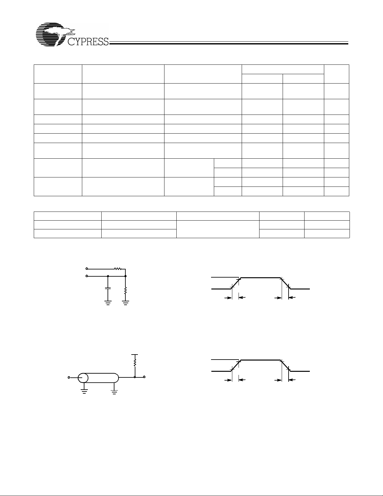
AC Test Loads and Waveforms (-10 & -15)
R1=330
3.3V
OUTPUT
CL=30 pF
INCLUDING
JIG AND
SCOPE
Ω
R2=680
ALL INPUT PULSES
3.0V
Ω
GND
≤
3ns
90%
10%
90%
10%
3
ns
≤
AC Test Loads and Waveforms (-7)
VCC/2
50Ω
I/O
Notes:
4. Input signals switch from 0V to 3V with a rise/fall time of less than 3 ns, clocks and clock enables switch at 20 MHz, while data inputs switch at 10 MHz. Outputs
are unloaded.
5. All inputs = V
6. Tested initially and after any design or process changes that may affect these parameters.
CC
Z0=50
Ω
– 0.2V, except RCLK and WCLK (which are at frequency = 0 MHz). All outputs are unloaded.
3.0V
GND
≤
3ns
ALL INPUT PULSES
90%
10%
90%
10%
3
ns
≤
7
PRELIMINARY
CY7C43646AV
CY7C43666AV/CY7C43686AV
Switching Characteristics
Over the Operating Range
7C43646/
66/86AV
-7
7C43646/
66/86AV
-10
7C43646/
66/86AV
-15
Parameter Description
f
S
t
CLK
t
CLKH
t
CLKL
t
DS
t
ENS
Clock Frequency, CLKA, CLKB, or CLKC 133 100 67 MHz
Clock Cycle Time, CLKA, CLKB, or CLKC 7.5 10 15 ns
Pulse Duration, CLKA, CLKB, or CLKC HIGH 3.5 4 6 ns
Pulse Duration, CLKA, CLKB, or CLKC LOW 3.5 4 6 ns
Set-Up Time, A
C
before CLKC↑
0–17
Set-Up Time, CSA, W/RA, ENA, and MBA before CLKA↑;
before CLKA↑, B
0–35
before CLKB↑, and
0–17
3 4 5 ns
3 4 5 ns
RENB and MBB before CLKB↑, and WENC and MBC before
CLKC↑
t
RSTS
t
FSS
t
BES
t
SPMS
t
SDS
t
SENS
t
FWS
t
DH
t
ENH
t
RSTH
t
FSH
t
BEH
t
SPMH
t
SDH
t
SENH
t
SPH
t
SKEW1
t
SKEW2
Set-Up Time, MRS1, MRS2, PRS1, or PRS2 LOW before
CLKA↑ or CLKB↑
[7]
2.5 4 5 ns
Set-Up Time, FS0 and FS1 before MRS1 and MRS2 HIGH 5 7 7.5 ns
Set-Up Time, BE/FWFT before MRS1 and MRS2 HIGH 5 7 7.5 ns
Set-Up Time, SPM before MRS1 and MRS2 HIGH 5 7 7.5 ns
Set-Up Time, FS0/SD before CLKA↑ 3 4 5 ns
Set-Up Time, FS1/SEN before CL K A↑ 3 4 5 ns
Set-U p Tim e, FW FT b efore CL K A↑ 0 0 0 ns
Hold Time, A
C
before CLKC↑
0–17
Hold Time, CSA, W/RA, ENA, and MBA before CLKA↑; RENB
before CLKA↑, B
0–35
before CLKB↑, and
0–17
0 0 0 ns
1 2 0 ns
and MBB before CLKB↑, and WENC and MBC before CLKC↑
Hold Time, MRS1, MRS 2, PRS1, or PRS2 LOW after CLKA↑
or CLKB↑
[7]
1 1 4 ns
Hold Time, FS0 and FS1 after MRS1 and MRS2 HIGH 1 1 2 ns
Hold Time, BE/FWFT after MRS1 and MRS2 HIGH 0 0 2 ns
Hold Time, SPM after MRS1 and MRS2 HIGH 0 0 2 ns
Hold Time, FS0/SD after CLKA↑ 0 1 0 ns
Hold Time, FS1/SEN after CLKA↑ 5 5 0 ns
Hold Time, FS1/SEN HIGH after MRS1 and MRS2 HIGH 2 2 2 ns
[8]
Skew Time between CLKA↑ and CLKB↑ for EFA/ORA,
EFB
/ORB, FFA/IRA, and FFC/IRC
[8]
Skew Time between CLKA↑ and CLKB↑ f or AEA, AEB, AFA,
7.5 7.5 7.5 ns
7 8 12 ns
AFC
t
A
t
WFF
t
REF
t
PAE
t
PAF
Notes:
7. Requirement to count the clock edge as one of at least four needed to reset a FIFO.
8. Ske w time is not a timing constraint for proper device operation and is only included to illustrate the timing relationship between the CLKA cycle and the CLKB
cycle.
Access Time, CLKA↑ to A
Propagation Delay Time, CLKA↑ to FFA/IRA and CLKB↑ to
FFC
/IRC
Propagation Delay Time, CLKA↑ to EFA/ORA and CLKB↑ to
EFB
/ORB
and CLKB↑ to B
0–35
0–17
1 6 1 8 3 10 ns
1 6 1 8 2 10 ns
1 6 1 8 1 10 ns
Propagation Delay Time, CLKA↑ to AEA and CLKB↑ to AEB 1 6 1 8 1 10 ns
Propagation Delay Time, CLKA↑ to AFA and CLKC↑ to AFC 1 6 1 8 1 10 ns
UnitMin. Max. Min. Max. Min. Max.
8
PRELIMINARY
CY7C43646AV
CY7C43666AV/CY7C43686AV
Switching Characteristics
Over the Operating Range (continued)
Parameter Description
t
PMF
t
PMR
t
MDV
t
RSF
t
EN
t
DIS
t
PRT
t
RTR
Notes:
9. Writing data to the Mail1 register when the B
10. Writing data to the Mail2 register when the A
Propagation De lay Time, CLKA↑ to MBF1 LOW or MBF2 HIGH
and CLKB↑ to MBF2
Propagation Delay Time, CLKA↑ to B
[10]
A
0–35
LOW or MBF1 HIGH
Propagation Dela y Time, MBA to A
Valid
Propagation Delay Time, MRS1 or PRS1 LOW to AEB LOW,
AFA
HIGH, FF A / IRA LO W, EFB /ORB LOW and MBF1 HIGH
and MRS2
LOW, EFA
or PRS2 LOW to AEA LOW, AFC HIGH, FFC / IRC
/ORA LOW and MBF2 HIGH
Enable Time, CSA or W/RA LOW to A
LOW and RENB HIGH to B
0–17
Active
Disable Time , CSA or W/RA HIGH to A
and CSB
HIGH or RENB LOW to B
Retransmit Pulse W idth 60 60 60 ns
Retransmit Recov ery Time 90 90 90 ns
outputs are active and MBB is HIGH.
0–17
outputs are active and MBA is HIGH.
0–35
[9]
and CLKB↑ to
0–17
valid and MBB to B
0–35
Active and CS B
0–35
at High Impedance
0–35
at High Impedance
0–17
0–17
7C43646/
66/86AV
-7
7C43646/
66/86AV
-10
7C43646/
66/86AV
-15
1 7 2 11 0 10 ns
1 6 2 9 3 12 ns
1 6 1 10 3 11 ns
1 5 2 8 1 15 ns
1 5 1 6 2 10 ns
1 8 1 8 1 8 ns
UnitMin. Max. Min. Max. Min. Max.
9

PRELIMINARY
Switching Waveforms
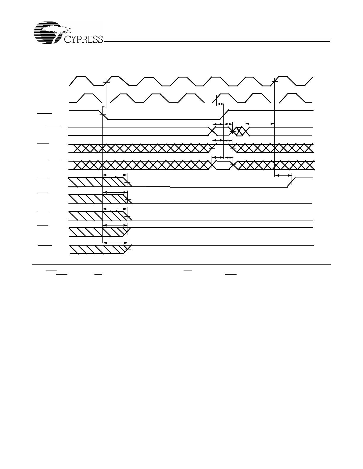
FIFO1 Master Reset Loading X1 and Y1 with a Preset Value of Eight
CLKA
CLKB
t
RSTS
CY7C43646AV
CY7C43666AV/CY7C43686AV
[11, 12]
t
RSTS
MRS1
t
BES
t
BEH
BE/FWFT
t
SPMS
t
SPMH
SPM
t
FSS
t
FSH
FS1, FS0
t
RSF
/IRA
FFA
t
t
RSF
RSF
EFB
/ORB
AEB
t
RSF
AFA
t
RSF
MBF1
Notes:
11. PRS1
12. If BE/FWFT is HIGH, then EFB/ORB will go LOW one CLKB cycle earlier than the case where BE/FWFT is LOW.
and MBC must be HIGH during Master Reset until the rising edge of FFA/IRA goes HIGH.
t
FWS
t
WFF
10
PRELIMINARY
CY7C43646AV
CY7C43666AV/CY7C43686AV
Switching Waveforms
(continued )
FIFO2 Master Reset Loading X1 and Y1 with a Preset Value of Eight
CLKC
CLKA
t
RSTS
MRS2
BE/FWFT
SPM
FS1/SEN,
FS0/SD
FFC
/IRC
EFA
/ORA
t
t
t
RSF
RSF
RSF
AEB
t
RSF
AFA
t
SPMS
t
t
BES
FSS
[13, 14]
t
RSTS
t
BEH
t
SPMH
t
FSH
t
FWS
t
WFF
t
RSF
MBF2
Notes:
13. PRS2
14. If BE/FWFT is HIGH, then EFA/ORA will go LOW one CLKA cycle earlier than the case where BE/FWFT is LOW.
and MBC must be HIGH during Master Reset until the rising edge of FFC/IRC goes HIGH.
11
PRELIMINARY
CY7C43646AV
CY7C43666AV/CY7C43686AV
Switching Waveforms
(continued )
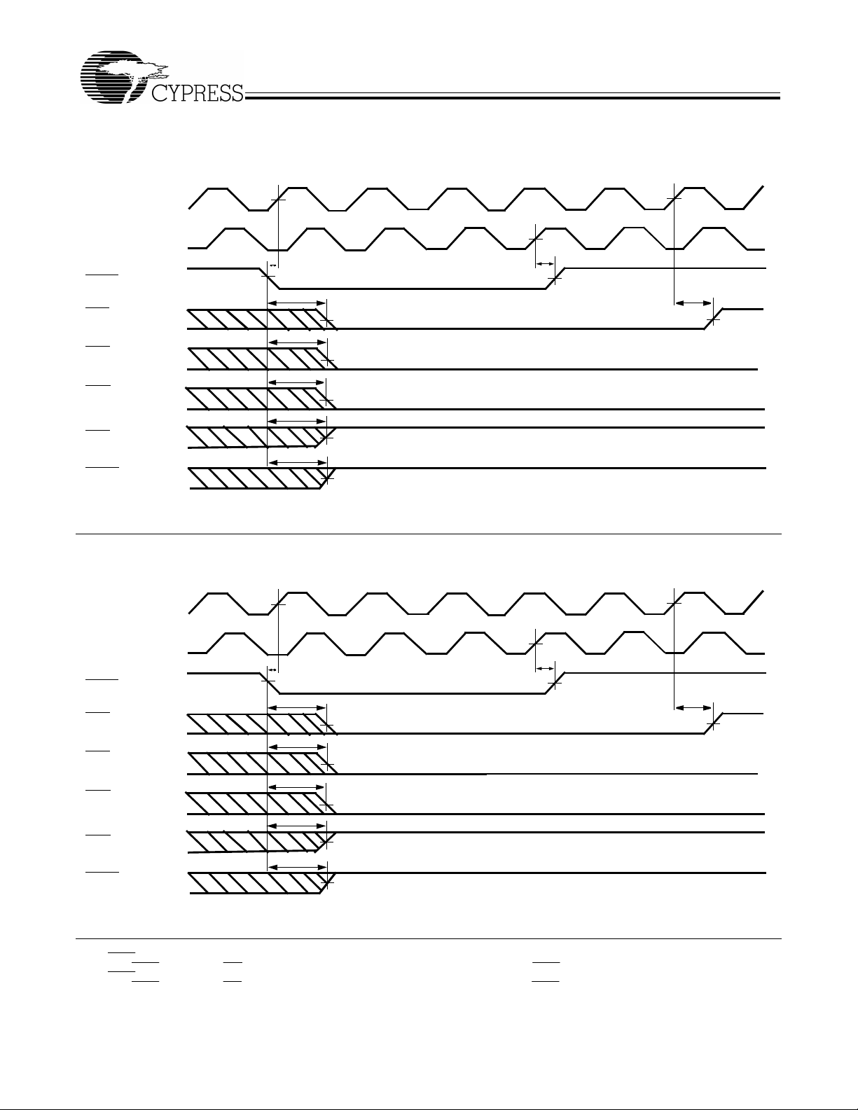
FIFO1 Partial Reset (CY Standard and FWFT Modes)
CLKA
CLKB
t
RSTS
PRS1
t
RSF
FFA/IRA
t
RSF
EFB
/ORB
t
RSF
AEB
t
RSF
AFA
t
RSF
MBF1
[15, 16]
t
RSTH
t
WFF
FIFO2 Partial Reset (CY Standard and FWFT Modes)
[17, 18]
CLKC
CLKA
t
RSTS
t
RSTH
PRS2
t
RSF
FFC/IRC
t
RSF
EFA
/ORA
t
RSF
AEA
t
RSF
AFC
t
RSF
MBF1
Notes:
15. MRS1
16. If BE/FWFT is HIGH, then EFB/ORB will go LOW one CLKB cycle earlier than the case where BE/FWFT is LOW.
17. MRS2 must be HIGH during Partial Reset.
18. If BE/FWFT is HIGH, then EFA/ORA will go LOW one CLKA cycle earlier than the case where BE/FWFT is LOW.
must be HIGH during Partial Reset.
t
WFF
12

PRELIMINARY
CY7C43646AV
CY7C43666AV/CY7C43686AV
Switching Waveforms
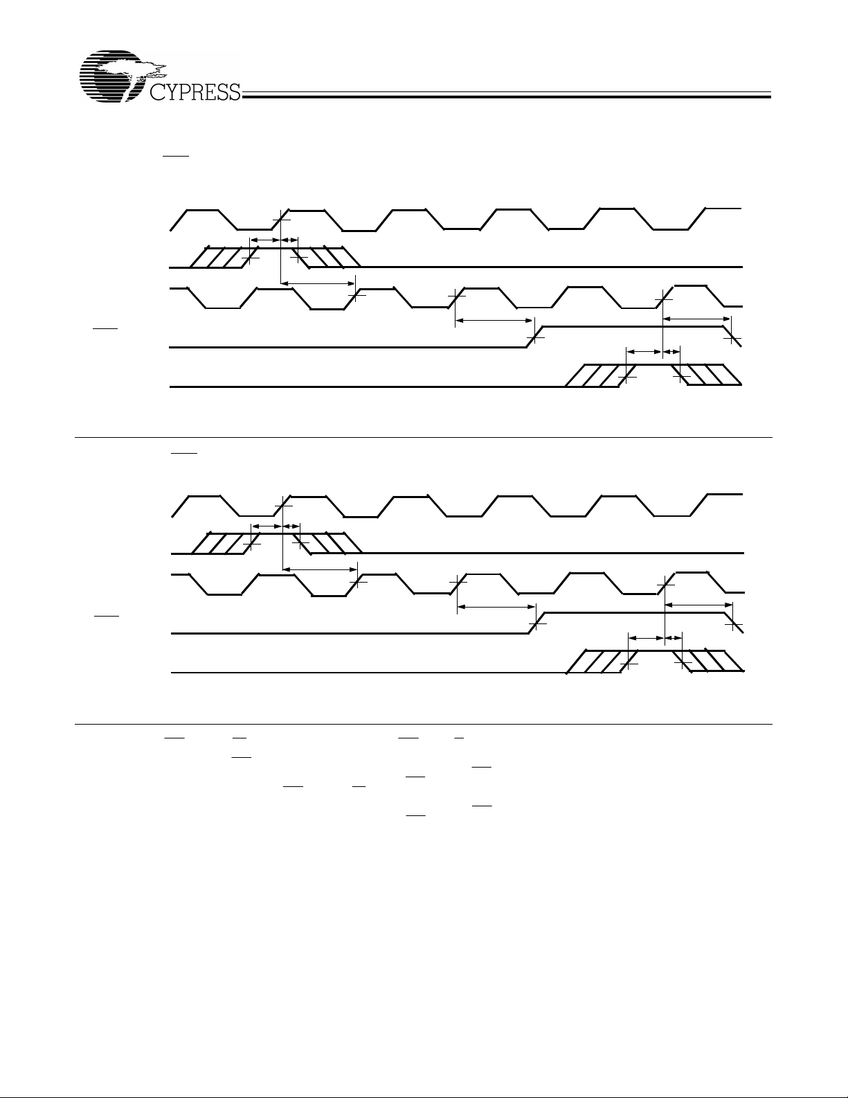
Parallel Program ming of the Almost-Full Flag and Almost-Empty Flag Off set Values after Reset
(CY Standard and FWFT Modes)
(continued )
[19]
CLKA
, MRS2
MRS1
t
FSS
t
FSH
SPM
t
FSS
t
FSH
FS1/SEN,
FS0/SD
FFA/
IRA
t
WFF
t
ENS
t
ENH
ENA
t
DH
DS
AEA
AEB Offset (X1)
AFC
Offset (Y2)
Offset (X2)
A
0 − 35
t
AFA Offset (Y1)
CLKB
FFC
/IRC
[20]
t
SKEW1
First Word to FIFO1
Serial Programming of the Almost -Full Flag and Almost-Empty Flag
Offset Values (CY Standard and FWFT Modes)
[21]
CLKA
MRS1, MRS2
t
t
FSH
FSS
SPM
t
WFF
[22]
t
SENS
t
SENH
SKEW1
FFA/IRA
t
FSS
t
SPH
t
SENS
t
SENH
t
FS1/SEN
FS0/SD
[23]
t
SDS
AFA Offset (Y1) MSB
t
SDH
t
SDS
AEA Offset (X2) LSB
t
SDH
CLKB
t
WFF
FFA/
IRA
Notes:
19. CSA
20. t
21. It is not necessary to program offset register bits on consecutive clock cycles. FIFO write attempts are ignored until IRA is set HIGH.
22. t
23. Programmable offsets are written serially to the SD input in the order AFA
=LOW, W/RA=HIGH, MBA=LOW. It is not necessary to program offset register on consecutive clock cycles.
is the minimum time between the rising CLKA edge and a rising CLKB for FFC/IRC to transition HIGH in the next cycle. If the time between the rising
SKEW1
edge of CLKA and rising edge of CLKC is less than t
is the minimum time between the rising CLKA edge and a rising CLKC for FFC/IRC to transition HIGH in the next cycle. If the time between the rising
SKEW1
edge of CLKA and rising edge of CLKC is less than t
, then FFC/IRC may transition HIGH one cycle later than shown.
SKEW1
, then FFC/IRC may transition HIGH one cycle later than shown.
SKEW1
offset (Y1), AEB offset (X1), AFC offset (Y2), and AEA offset (X2).
13

PRELIMINARY
CY7C43646AV
CY7C43666AV/CY7C43686AV
Switching Waveforms
(continued )
Port A Write Cycle Timing for FIFO1 (CY Standard and FWFT Modes)
t
CLK
t
CLKH
t
CLKL
CLKA
FFA/
IRA
HIGH
t
ENStENH
CSA
t
ENStENH
W/RA
t
t
ENH
ENS
MBA
t
t
ENH
ENS
ENA
t
t
DS
DH
A
0–35
W1
[24]
t
W2
ENS
[24]
t
ENH
t
ENS
t
ENH
Port C Wo rd Write Cycle Timing for FIFO2 (CY Stand ard and FWFT Modes)
CLKC
/IRC
FFC
HIGH
t
ENStENH
t
ENS
t
ENH
MBC
t
ENS
t
ENH
t
ENS
t
ENH
WENC
tDSt
C
0–17
Note:
24. Written to FIFO1
DH
14

PRELIMINARY
CY7C43646AV
CY7C43666AV/CY7C43686AV
Switching Waveforms
(continued )
Port C Byte Write Cycle Timing for FIFO2 (CY Standard and FWFT Modes)
CLKC
/IRC
FFC
HIGH
t
ENS
t
ENH
MBC
t
t
ENH
ENS
WENC
t
t
DS
DH
C
0–8
t
ENS
t
t
ENH
ENH
Port B Byte Read Cycle Timing f or FIFO1 (CY Standard and FWFT Modes)
CLKB
/ORB
EFB
HIGH
CSB
MBB
t
t
ENS
ENH
RENB
Read 1
t
Read 2
t
A
A
Read 2
Read 3
t
A
t
A
B
0–8
(Standard Mode)
OR
B
0–8
(FWFT Mode)
Note:
25. Unused bytes B
t
MDV
t
EN
Previous Data
t
MDV
t
EN
Read 1
contain all zeroes for byte-size reads.
9–17
t
A
t
A
[25]
Read 3
Read 4
t
A
t
A
No Operation
Read 4
Read 5
t
DIS
t
DIS
15

PRELIMINARY
CY7C43646AV
CY7C43666AV/CY7C43686AV
Switching Waveforms
(continued )
Port B W ord Read Cycle Timing for FIFO1 (CY Standard and FWFT Modes)
CLKB
/ORB
EFB
CSB
MBB
t
t
ENH
ENS
ENB
B
0–17
(Standard Mode)
OR
B
0–17
(FWFT Mode)
t
t
MDV
MDV
t
EN
t
EN
t
A
Previous Data
t
A
Read 1
Read 1
Read 2
t
A
t
A
No Operation
Read 2
Read 3
t
DIS
t
DIS
Port A Read Cycle Timing for FIFO2 (CY Standard and FWFT Modes)
t
CLK
t
CLKH
t
CLKL
CLKA
EFA
/ORA
CSA
W/RA
MBA
t
t
ENS
ENH
ENA
W1
[26]
t
A
W1
t
A
W2
A
0−35
(Standard Mode)
OR
A
0−35
(FWFT Mode)
Note:
26. Read from FIFO2.
t
MDV
t
EN
Previous Data
t
MDV
t
EN
[26]
[26]
t
ENS
t
ENH
t
ENStENH
t
A
t
A
No Operation
[26]
W2
[26]
W3
t
DIS
t
DIS
16

PRELIMINARY
CY7C43646AV
CY7C43666AV/CY7C43686AV
Switching Waveforms
(continued )
ORB Flag Timing and First Data Word Fall Through when FIFO1 is Empty (FWFT Mode)
t
CLK
t
t
CLKH
CLKL
CLKA
CSA
W/RA
LOW
HIGH
t
ENS
t
EN
MBA
t
t
ENS
EN
ENA
FFA
A
0–35
CLKB
EFB
/IRA
/ORB
HIGH
FIFO1 Empty
t
t
DH
DS
W1
[28]
t
t
SKEW1
CLKH
t
CLK
t
CLKL
t
REF
t
[27]
REF
CSB
MBB
LOW
LOW
RENB
t
A
B
0–17
Notes:
27. If Port B size is word or byte, ORB is set LOW by the last word or byte read from FIFO2, respectively.
28. t
is the minimum time between a rising CLKA edge and a rising CLKB edge for ORB to transition HIGH and to clock the next word to the FIFO1 output
SKEW1
register in three CLKB cycles. If the time between the rising CLKA edge and rising CLKB edge is less than t
load of the first word to the output register may occur one CLKB cycle later than shown.
Old Data in FIFO1 Output Register
t
ENStENH
W1
, then the transition of ORB HIGH and
SKEW1
17

PRELIMINARY
CY7C43646AV
CY7C43666AV/CY7C43686AV
Switching Waveforms
(continued )
EFB Flag Timing and First Data Read F all Through when FIFO1 is
Empty (CY Standard Mode)
[29]
t
CLKA
CSA
W/RA
LOW
HIGH
t
ENS
t
ENH
MBA
t
t
ENS
ENH
ENA
/IRA
FFA
A
0–35
HIGH
t
DS
W1
t
DH
t
SKEW1
[30]
t
CLKH
t
CLKL
CLKB
t
REF
EFB
/ORB
FIFO1 Empty
t
CLK
CLKH
t
CLK
t
CLKL
t
REF
CSB
MBB
LOW
LOW
RENB
B
0–17
Notes:
29. If Port B size is word or byte, EFB
30. t
is the minimum time between a rising CLKA edge and a rising CLKB edge for EFB to transition HIGH in the next CLKB cycle. If the time between
SKEW1
the rising CLKA edge and rising CLKB edge is less than t
is set LOW by the last word or byte read from FIFO1, respectively.
t
t
ENS
ENH
t
A
W1
, then the transition of EFB HIGH may occur one CLKB cycle later than shown.
SKEW1
18

PRELIMINARY
CY7C43646AV
CY7C43666AV/CY7C43686AV
Switching Waveforms
(continued )
ORA Flag Timing and First Data Word Fall Through when FIFO2 is Empty
(FWFT Mode)
[31]
t
CLK
t
CLKHtCLKL
CLKC
WENC
FFC
C
0–17
/IRC
HIGH
t
t
DH
DS
W1
[32]
t
t
SKEW1
CLKH
t
CLKL
CLKA
t
CLK
EFA
/ORA
CSA
FIFO2 Empty
LOW
t
REF
t
REF
W/RA
MBA
LOW
LOW
ENA
t
A
A
0–35
Notes:
31. If Port B size is word or byte, t
32. t
is the minimum time between a rising CLKC edge and a rising CLKA edge for ORA to transition HIGH and to clock the next word to the FIFO2 output
SKEW1
register in three CLKA cycles. If the time between the rising CLKC edge and rising CLKA edge is less than t
load of the first word to the output register may occur one CLKA cycle later than shown.
Old Data in FIFO2 Output Register
is referenced to the rising CLKC edge that writes the last word or byte of the long word, respectively.
SKEW1
t
ENStENH
W1
, then the transition of ORA HIGH and
SKEW1
19

PRELIMINARY
CY7C43646AV
CY7C43666AV/CY7C43686AV
Switching Waveforms
Flag Timing and First Data Read when FIFO2 is Empty (CY Standard Mode)
EFA
CLKC
MBC
WENC
FFC
C
0–17
CLKA
EFA
CSA
/IRC
/ORA
HIGH
FIFO2 Empty
LOW
(continued )
t
t
ENH
ENS
t
t
ENH
ENS
t
t
DH
DS
W1
t
SKEW1
[34]
t
CLKHtCLKL
t
CLK
t
CLK
t
CLKHtCLKL
t
REF
t
[33]
REF
W/RA
MBA
LOW
LOW
ENA
A
0–35
Notes:
33. If Port C size is word or byte, t
34. t
is the minimum time between a rising CLKC edge and a rising CLKA edge for EFA to transition HIGH in the next CLKA cycle. If the time between
SKEW1
the rising CLKC edge and rising CLKA edge is less than t
is referenced to the rising CLKC edge that writes the last word or byte of the long word, respectively.
SKEW1
t
ENStENH
t
A
W1
, then the transition of EFA HIGH may occur one CLKA cycle later than shown.
SKEW1
20

PRELIMINARY
CY7C43646AV
CY7C43666AV/CY7C43686AV
Switching Waveforms
(continued )
IRA Flag Timing and First Available Write when FIFO1 is Full (FWFT Mode)
t
CLK
t
t
CLKH
CLKL
CLKB
CSB
LOW
MBB
t
t
ENH
ENS
RENB
/ORB
EFB
B
0–17
HIGH
t
A
Previ ou s Word in FI FO1 Output Register
t
SKEW1
Next Word From FIFO1
[36]
t
CLKH
t
CLKL
CLKA
t
WFF
FFA
/IRA
FIFO1 Full
t
CLK
t
[35]
WFF
CSA
W/RA
LOW
HIGH
MBA
ENA
A
0–35
Notes:
35. If Port B size is word or byte, t
36. t
is the minimum time between a rising CLKB edge and a rising CLKA edge for IRA to transition HIGH in the next CLKA cycle. If the time between the
SKEW1
rising CLKB edge and rising CLKA edge is less than t
is referenced to the rising CLKB edge that reads the last word or byte write of the long word, respectively.
SKEW1
t
t
ENH
ENS
t
ENStENH
t
t
DS
DH
To FIFO1
, then IRA may transition HIGH one CLKA cycle later than shown.
SKEW1
21

PRELIMINARY
CY7C43646AV
CY7C43666AV/CY7C43686AV
Switching Waveforms
(continued )
FFA Flag Timing and First A vailable Write when FIFO1 is Full (CY Stan dard Mode)
t
CLK
t
t
CLKH
CLKL
CLKB
CSB
LOW
MBB
t
ENStENH
RENB
/ORB
EFB
B
0–17
HIGH
t
A
Previous Word in FIFO1 Output Register
t
SKEW1
Next Word From FIFO1
[37]
t
CLKH
t
CLKL
CLKA
t
WFF
FFA
/IRA
FIFO1 Full
t
CLK
t
WFF
[35]
Read Disabled
CSA
W/RA
LOW
HIGH
MBA
ENA
A
0−35
Note:
37. t
is the minimum time between a rising CLKB edge and a rising CLKA edge for FFA to transition HIGH in the next CLKA cycle. If the time between the
SKEW1
rising CLKB edge and rising CLKA edge is less than t
t
t
ENH
ENS
t
t
ENS
ENH
tDHt
DS
, then the transition of FFA HIGH may occur one CLKA cycle later than shown.
SKEW1
22

PRELIMINARY
CY7C43646AV
CY7C43666AV/CY7C43686AV
Switching Waveforms
(continued )
IRC Flag Timing and First Available Write when FIFO2 is Full (FWFT Mode)
t
CLK
t
t
CLKH
CLKL
CLKA
CSA
W/RA
MBA
LOW
LOW
LOW
t
ENS
t
ENH
ENA
EFA
A
0–35
/ORA
HIGH
t
A
Previo us Word i n FIFO2 O ut put Register
t
SKEW1
Next Word From FIFO2
[39]
t
CLKH
t
CLKL
CLKC
t
WFF
FFC
/IRC
FIFO2 Full
t
CLK
t
[38]
WFF
t
t
ENH
ENS
MBC
t
t
ENH
ENS
WENC
tDHt
DS
C
0–17
To FIFO2
Notes:
38. If Port C size is word or byte, IRC is set LOW by the last word or byte write of the long word, respectively.
39. t
is the minimum time between a rising CLKA edge and a rising CLKC edge for IRC to transition HIGH in the next CLKB cycle. If the time between the
SKEW1
rising CLKA edge and rising CLKC edge is less than t
, then the transition of IRC HIGH may occur one CLKC cycle later than shown.
SKEW1
23

PRELIMINARY
CY7C43646AV
CY7C43666AV/CY7C43686AV
Switching Waveforms
(continued )
FFC Flag Timing and First Available Write when FIFO2 is Full (CY Standard Mode)
t
CLK
t
t
CLKH
CLKL
CLKA
CSA
W/RA
MBA
LOW
LOW
LOW
t
ENS
t
ENH
ENA
EFA
A
0–35
/IRA
HIGH
t
A
Previous Word in FIFO12 Output Register
t
SKEW1
Next Word From FIFO2
[41]
t
CLKH
t
CLKL
CLKC
t
ENS
t
ENH
t
WFF
FFC
/IRC
FIFO2 Full
t
CLK
t
WFF
MBC
t
ENStENH
ENB
tDHt
DS
C
0–17
To FIFO2
[40]
Notes:
40. If Port C size is word or byte, FFC
41. t
is the minimum time between a rising CLKA edge and a rising CLKB edge for FFC to transition HIGH in the next CLKB cycle. If the time between
SKEW1
the rising CLKA edge and rising CLKC edge is less than t
is set LOW by the last word or byte write of the long word, respectively.
, then the transition of FFC HIGH may occur one CLKC cycle later than shown.
SKEW1
24
PRELIMINARY
CY7C43646AV
CY7C43666AV/CY7C43686AV
Switching Waveforms
Timing for AEB
CLKA
ENA
CLKB
AEB
RENB
Timing for AEA
CLKC
WENC
CLKA
AEA
ENA
when FIFO2 is Almost Empty (CY Standard and FWFT Modes)
X1 Word in FIFO1
when FIFO2 is Almost Empty (CY Standard and FWFT Modes)
X2 Word in FIFO2
(continued )
t
ENS
t
ENS
t
ENH
t
SKEW2
t
ENH
t
SKEW2
[47]
[44]
t
PAE
t
PAE
[42, 43]
(X1+1)Words in FIFO1
t
ENS
[45, 46]
(X2+1)Words in FIFO2
t
ENS
t
t
ENH
t
PAE
t
PAE
ENH
Notes:
42. FIFO1 Write (CSA
read from the FIFO.
43. If Port B size is word or byte, AEB is set LOW by the last word or byte read from FIFO1, respectively.
44. t
45. FIFO2 Write (MBB = LOW), FIFO2 read (CSA
46. If Port C size is word or byte, t
47. t
is the minimum time between a rising CLKA edge and a rising CLKB edge for AEB to transition HIGH in the next CLKB cycle. If the time between
SKEW2
the rising CLKA edge and rising CLKB edge is less than t
is the minimum time between a rising CLKC edge and a rising CLKA edge for AEA to transition HIGH in the next CLKA cycle. If the time between
SKEW2
the rising CLKC edge and rising CLKA edge is less than t
= LOW , W/RA = LOW, MBA = LOW), FIFO1 read (CSB = LOW, W/RB = HIGH, MBB = LOW). Data in the FIFO1 output register has been
, then AEB may transition HIGH one CLKB cycle later than shown.
= LOW, W/RA = LOW, MBA = LOW). Data in the FIFO2 output register has been read from the FIFO.
is referenced to the rising CLKC edge that writes the last word or byte of the long word, respectively.
SKEW2
SKEW2
, then AEA may transition HIGH one CLKA cycle later than shown.
SKEW2
25

PRELIMINARY
CY7C43646AV
CY7C43666AV/CY7C43686AV
Switching Waveforms
(continued )
Timing for AFA when FIFO1 is Almost Full (CY Standard and FWFT Modes)
[51]
t
SKEW2
CLKA
t
ENS
t
ENH
ENA
t
AFA
CLKB
[D–(Y1+1)] Words in FIFO1
PAF
(D–Y1)Words in FIFO1
t
ENS
ENH
t
RENB
Timing for AFC
CLKC
when FIFO2 is Almost Full (CY Standard and FWFT Modes)
[53]
t
SKEW2
t
t
ENS
ENH
WENC
t
PAF
AFC
[D–(Y2+1)] Words in FIFO2
(D–Y2)Words in FIFO2
[48, 49, 50 ]
[45, 49, 52 ]
t
PAF
t
PAF
CLKA
t
t
ENS
ENH
ENA
Notes:
48. FIFO1 Write (CSA
FIFO.
49. D = Maximum FIFO Depth =1K for the CY7C43646AV, 4K for the CY7C43666AV, and 16K for the CY7C43686AV.
50. If Port B size is word or byte, t
51. t
52. If Port C size is word or byte, AFC
53. t
is the minimum time between a rising CLKA edge and a rising CLKB edge for AFA to transition HIGH in the next CLKA cycle. If the time between the
SKEW2
rising CLKA edge and rising CLKB edge is less than t
is the minimum time between a rising CLKC edge and a rising CLKA edge for AFC to transition HIGH in the next CLKC cycle. If the time between
SKEW2
the rising CLKC edge and rising CLKA edge is less than t
= LOW , W/RA = HIGH, MBA = LOW), FIFO1 read (CSB = LOW, MBB = LOW). Data in the FIFO1 output register has been read from the
is referenced to the rising CLKB edge that writes the last word or byte of the long word, respectively .
SKEW2
, then AFA may transition HIGH one CLKB cycle later than shown.
is set LOW by the last word or byte write of the long word, respectively.
SKEW2
SKEW2
, then AFC may transition HIGH one CLKA cycle later than shown.
26

PRELIMINARY
CY7C43646AV
CY7C43666AV/CY7C43686AV
Switching Waveforms
(continued )
Timing for Mail1 Register and MB F1
CLKA
CSA
W/RA
MBA
ENA
A
0–35
CLKB
MBF1
CSB
t
ENS
t
ENS
t
ENS
t
DS
Flag (CY Standard and FWFT Modes)
t
t
ENH
ENS
t
ENH
t
ENH
t
ENH
t
DH
W1
t
PMF
[54]
t
PMF
MBB
RENB
t
EN
B
0–17
Note:
54. If Port B is configured for word size, data can be written to the Mail1 register using A
data). If Port B is configured for byte size, data can be written to the Mail1 Register using A
have valid data (B
will be indeterminate).
9–17
FIFO1 Output Register
t
MDV
t
PMR
t
ENS
W1 (Remains valid in Mail1 Register after read)
(A
0–17
are don’t care inputs). In this first case B
18–35
(A
0–8
are don’t care inputs). In this second case, B
9–35
t
ENH
t
DIS
will have valid
0–17
0–8
will
27

PRELIMINARY
CY7C43646AV
CY7C43666AV/CY7C43686AV
Switching Waveforms
(continued )
Timing for Mail2 Register and MBF2 Flag (CY Standard and FWFT Modes)
CLKC
MBC
t
t
ENH
ENS
WENC
t
t
DH
DS
C
0–17
W1
CLKA
t
PMF
MBF2
CSA
W/RA
MBA
ENA
t
MDV
t
PMR
A
0−35
t
EN
FIFO2 Output Register
[55]
t
PMF
t
ENS
W1 (Remains valid in Mail2 Register after read)
t
ENH
t
DIS
FIFO1 Retransmit Timing
[56, 57, 58, 59]
RT1
t
PRT
t
RTR
RENB
EFB/FFA
Notes:
55. If Port C is configured for word size, data can be written to the Mail2 register using C
indeterminate). If Port C is configured for byte size, data can be written to the Mail2 Register using B
A
will have valid data (A
0–8
56. Retransmit is performed in the same manner for FIFO2.
57. Clocks are free running in this case.
58. The flags may change state during Retransmit as a result of the offset of the read and write pointers, but flags will be valid at t
59. For the synchronous PAE and PAF flags (SMODE), an appropriate c loc k cycle i s nec essary after t
will be indeterminate).
9–35
. In this first case A
0–17
to update the se flags .
RTR
0–8
will have valid data (A
0–17
(B
are don’t care inputs). In this second case,
9–17
28
RTR
will be
18–35
.

PRELIMINARY
CY7C43646AV
CY7C43666AV/CY7C43686AV
Signal Description
Master Reset (MRS1, MRS2)
Each of the t wo FIFO memories of the CY7C436X6AV undergoes a complete reset by taking its associated Master Reset
, MRS2) input LO W f or at least f our P ort A cl ock (CLKA)
(MRS1
and four Port B clock (CLKB) LOW-to-HIGH transitions. The
Master Reset inputs can swit ch asynchronously to the clocks .
A Master Reset initializes the internal read and write pointers
and for ces the Full/In put Ready flag (FFA
the Empty/Output Ready flag (EF A
Almost Empty flag (AEA
(AFA
, AFC) HIGH. A Master Reset also f orces the Mai lbox f lag
(MBF1
, MBF2) of the parallel mailbox register HIGH. After a
Master Reset, the FIFO’s Full/Input Ready flag is set HIGH
after tw o cloc k cycles to beg in normal oper ati on. A Master Reset must be p erformed on the FIF O after po wer up , bef ore data
is written to its memory.
A LOW-to-HIGH transition on a FIFO Master Reset (MRS1
MRS2
) input latches the value of the Big Endian (BE) input or
determining the or der by which bytes are transferred through
Port B.
A LOW-to-HIGH transition on a FIFO reset (MRS1
input latches the values of the Flag select (FS0, FS1) and Serial Programming Mode (SPM
Full and Almost Empty offset programming method (see Almost Empty and Almost Full fl ag offset programming below).
Partial Reset (PRS1
Each of the t wo FIFO memories of the CY7C436X6AV undergoes a limited reset by taking its associated Partial Reset
, PRS2) input LO W fo r at l east four Port A clock (CLKA)
(PRS1
and four Port B clock (CLKB) LOW-to-HIGH transitions. The
Partial Reset inputs can switch asynchronously to the clocks.
A Partial Rest initializes the internal read and write pointers
and for ces the Full/In put Ready flag (FFA
the Empty/Output Ready flag (EF A
Almost Empty flag (AEA
(AFA
, AFC) HIGH. A Partial Reset also forces the Mailbox flag
(MBF1
, MBF2) of the parallel mailbox register HIGH. After a
Partial Reset, the FIFO’s Full/Input Ready flag is set HIGH
after two cl ock cycles to begin normal operation.
Whatever flag offsets, programming method (parallel or serial), and timing mode (FWFT or CY Standard mode) are currently selected at the time a Partial Reset is initiated, those
settings will remain unchanged upon completion of the reset
operation. A Partial Reset may be useful in the case where
reprogramming a FIFO following a Master Reset would be inconvenient.
Big Endian/First-Word Fall-Through (BE/FWFT
This is a dual-purpose pi n. At the time of Master Reset , the BE
select function is active, permitting a choice of big or little endian byte arrangement for data written to or read from Port B.
This selection determi nes the order by which byte s (or words)
of data ar e trans fe rred t hr ough t his po rt. Fo r the following illustrations, assume that a byte (or word) bus size has been selected for Port B. (Note that when Por t B is configured for a
long word si ze , the Big Endian f unc tion has no appl icat ion an d
the BE input is a “Don’t Care .”)
A HIGH on the BE/FWFT
and MRS2) inputs go from LOW to HIGH will select a Big En-
, AEB) LOW, and the Almost Full fla g
) inputs f or choosing the Alm ost
, PRS2)
, AEB) LOW, and the Almost Full fla g
input when the M aster Reset (M RS1
/IRA, FFC /IRC) LOW ,
/ORA, EFB/ORB) LOW, the
, MRS2)
/IRA, FFC /IRC) LOW ,
/ORA, EFB/ORB) LOW, the
)
dian arrangement. When data is moving in the direction from
Port A to Port B, the most significant byte (word) of the longword written to Port A will be read from Port B first; the least
significant b yte (word) of the long -word written to P ort A will be
read from Por t B last. When data is moving in the direction
from Port C to Port A, the by te (word) written to Port C first will
be read from Por t A as the most significant byte (word) of the
long-word; the byte (word) written to Por t C last will be read
from Port A as the least significant byte (word) of the longword.
A LOW on the BE/FWFT
and MRS2) inputs go from LOW to HIGH will select a Little
Endian arrangement. When data is moving in the direction
from Port A to Port B, the least significant byte (word) of the
long word written to Port A will be read from Port B first; the
most significant byte (word) of the long word written to Port A
will be read fr om Port B last. When dat a is movi ng in the direc tion from P ort C to Port A, the byte (word) written t o Port C first
will be read from port A as the least significant byte (word) of
,
the long-word; the byte (word) written to P ort C last will be read
from Port A as the most significant byte (word) of the longword.
After Master Reset, t he FWFT select func tion is activ e, permitting a choice between two possible timing modes: CY Standard Mode or First-Word Fall-Through (FWFT) Mode. Once
the Master R eset (MRS 1
BE/FWFT
CLKA (for FIFO1) and CLKC (for FIFO2) will select CY Standard Mode. This mode uses the Empty Flag function (EFA
EFB
the FIFO memory. It uses the Full Fl ag function (FFA
indicate whether or not the FIFO memory has any free space
for writing. In CY Standard Mode, every word read from the
FIFO, including the first, must be requested using a formal
read operation.
Once the Master Reset (MRS1
on the BE/FWFT
of CLKA (for FIFO1) and CLKB (for FIFO2) will select FWFT
Mode. This mode uses the Output Ready function (ORA,
ORB) to indicate whether or not there is va li d data at the data
outputs (A
(IRA, IRC) to indicate whether or not the FIFO memory has
any free space for writing. In the FWFT Mode, the first word
written to an empty FI FO goes direct ly to data outputs, no r ead
request necessary. Subsequent words must be accessed by
performing a f ormal r ead operation.
Followi ng Ma ster Reset, the level applied to the BE/FWFT
put to choose the desired timing mode must remain static
throughout the FIFO ope ration.
Programming the Almost Empty and Almost Full Flags
Four regi sters i n the CY7C436 X6A V are us ed to hold the offset
values fo r the Almost Empty and Almost Ful l flags. The P ort B
Almost Empty flag (AEB
Port A Almost Empty flag (AEA
The Pos t A Al m ost Full flag (AFA
and the Port C Almost Full flag (AF C
Y2. The index of each register name corresponds with preset
values during the reset of a FIFO, programmed in parallel using the FIFO’s Port A data inputs, or programmed in serial
using the Serial Data (SD) input (see Table 1).
input at the second LOW-to-HIGH transition of
) to indicat e whet her or not t here a re any wo rds present in
input during the next LOW -to-HI GH transi tion
or B
0–35
input when the Master Reset (MRS1
, MRS2) input is HIGH, a HIGH on the
, MRS2) input is HIGH, a LO W
). It also uses the Input Ready func tion
0–17
) offset register is labeled X1 and the
) offset register is labeled X2.
) offset regist er is labeled Y1
) offset regist er is label ed
,
, FFC) to
in-
29

PRELIMINARY
CY7C43646AV
CY7C43666AV/CY7C43686AV
To load a FIFO’s Almost Empty fl ag and Almost Full flag of fset
registers with one of the three preset values listed in Ta ble 1 ,
the Serial Program Mode (SPM
) and at least one of the flagselect inputs m ust be HIGH during the LOW -to-HIG H transition
of its Master Reset input (MRS1
load the preset v alue of 64 int o X1 and Y1, SPM
must be HIGH when FIFO1 r eset (MRS1
and MRS2). For example, to
, FS0 and FS1
) returns H IG H. Fl agoffset registers associated with FIFO2 are loaded with one of
the preset v alues i n the same w ay wi th Master Reset (MRS2
When using one of the preset values for the flag offsets, the
FIFOs can be reset simultaneously or at different times.
To program the X1, X2, Y1, and Y2 registers from Port A, perform a Master Reset on both FIFOs simultaneously with SPM
HIGH and FS0 and FS1 LOW during the LOW-to-HIGH transition of MRS1
and MRS2. After this reset is complete, the first
four writes to FIFO1 do not store data in RAM but load the
offset registers in the order Y1, X1, Y2, X2. The Port A data
inputs used by the offset registers are (A
(A
), for the CY7C436X6A V, respect ively. The highest num-
0–13
bered input is used as the most significant bit of the binary
0–9
), (A
0–11
), or
number in e ach case. Valid programming values for the registers range from 1 to 1012 f or the CY7C43 646AV; 1 to 4092 for
the CY7C43666A V ; 1 to 16380 fo r the CY7C43686A V. After all
the offset registers are programmed from Port A, the Port C
Full/Input Ready (FFC
/IRC) is set HIGH and both FIFOs begin
normal operation.
To program the X1, X2, Y1, and Y2 registers s erially, initiate a
Master Reset with SPM
LOW, FS0/SD LOW, and FS1/SEN
HIGH during t he LO W - to-HI GH tr ans ition of M RS1 and MRS2.
After this reset is complete, the X and Y register values are
loaded bit-wise through the FS0/SD input on each LOW-toHIGH transition of CLKA that the FS1/SEN
input is LOW. 40-,
48-, or 56- bit writes are needed to complete the prog ramming
for the CY7C436X6AV, respectively. The four registers are
written in the order Y1, X1, Y2, and, finally, X2. The first-bit
write stores the most significant bit of the Y1 register and the
last-bit write stores the least significant bit of the X2 register.
Each register value can be programmed from 1 to 1020
(CY7C43646AV), 1 to 4092 (CY7C43666AV), or 1 to 16380
(CY7C43686AV).
When the opt ion t o prog r am the o ffset r egist ers serial l y is chosen, the Port A Full/Input Ready (FFA
until all register bits are written. FFA
/IRA) flag remains LOW
/IRA is set HI GH by t he
LOW-to-HIGH transition of CLKA after the last bit is loaded to
allow normal FIFO1 operation. The Port C Full/Input ready
(FFC
/IRC) flag also remains LOW throughout the serial pro-
gramming process, until all register bits are written. FFC
/IRC
is set HIGH by the LOW-to-HIGH transition of CLKC after the
last bit is loade d to al low normal FIFO2 operation.
SPM
, FS0/SD, and FS1/SEN function the same way in both
CY Standard and FWFT modes.
FIFO Write/Read Operation
The state of the Port A data (A
A Chip Select (CSA
The A
CSA
lines are in the high-impedance state when either
0–35
or W/RA is HIGH. The A
when bo th CSA
) and Por t A Write/Read Select (W/RA).
and W/RA are LOW.
Data is loa ded into FIFO1 from the A
HIGH transition of CLKA when CSA
ENA is HIGH, MBA is LOW , and FF A
from FIFO2 to the A
outputs by a LOW- to-HIGH transitio n
0–35
) lines is controlled by Port
0–35
lines are active outputs
0–35
inputs on a LOW-to-
0–35
is LOW, W/RA is HIGH,
/IRA is HIGH. Data is read
of CLKA when CSA
is LOW, and EFA
is LOW, W/RA is LOW , ENA is HI GH, MBA
/ORA is HIGH (see Table 2). FIFO reads and
writes on Port A are independent of any concurrent Port B
operation.
The state of the Port B data (B
Port B Chip Select (CSB
B
lines are in the high-impedance state when either CSB
0–17
is HIGH or RENB is LOW. The B
).
when CSB
is LOW and RENB is HIGH.
) and P ort B Read select (RENB). The
Data is load ed into FIFO2 from the C
HIGH transition of CLKC when WENC is LOW, MBC is LOW,
and FFC
to the B
when CSB
EFB
/IRC is HIGH (see Tabl e 4). Data is read from FIFO1
outputs by a LOW-to-HIGH transition of CLKB
0–17
is LOW, RENB is HIGH, MBB is LOW, and
/ORB is HIGH (see Ta b le 3 ). FIFO reads on Port B and
) lines is controlled by the
0–17
lines are active outputs
0–17
inputs on a LOW-to-
0–17
writes to P ort C are independent of any concurrent Port A operation.
The set-up and hold t ime constraints to the port clocks for t h e
port Chip Selects and Write/Read sel ects are onl y for ena bling
write and read operations and are not related to high-impedance control of the data o utputs. If a port enabl e is LOW during
a clock cycle, the p ort’s Chip Select and Write/Read select
may change states during the set -up and hold time window of
the cycle.
When operating the FIFO in FWFT Mode with the Output
Ready flag LOW, the next word written i s autom atic ally sent to
the FIFO’s output register by the LOW-to-HIGH transition of
the port clock that sets the Output Ready flag HIGH, data residing in the F IFO’s memory array is cl oc ked t o t he out put reg -
ister only when a rea d is sel ec ted usi ng the p ort’s Chip Select,
Write/Read select, Enable, and Mailbox select.
When operating the FIFO in CY Standar d Mode , r egardle ss o f
whether the Empty Flag is LOW or HIGH, data residing in the
FIFO’s memory array is clocked to the output register only
when a read is selected using the port’s Chip Select,
Write/Read select, Enable, and Mailbox select.
Synchronized FIFO Flags
Each FIFO is synchronized to its port clock through at least
two flip-flop stages . This is done to improv e flag-sign al reliability by reducing the probability of the metastable events when
CLKA, CLKB, and CLKC operate asynchronously to one another. EFA
CLKA. EFB
FFC
/ORA, AEA, FFA/IRA, and A FA are synchronized to
/ORB and AEB are synchronized to CLKB.
/IRC and AFC are synchronized to CLKC. Ta b le 5 and
Ta ble 6 show the relationship of each port flag to FIFO1 and
FIFO2.
Empty/Output Ready Fla gs (EFA
/ORA, EFB/ORB)
These are dual-purpose flags. In the FWFT Mode, the Output
Ready (ORA, ORB) function is selected. When the Output
Ready flag is HIGH, new data is present in the FIFO output
register. When the Output Ready flag is LOW, the previous
data word is prese nt in the FIFO output register and att empted
FIFO reads are ignored.
In the CY Standard Mode , the Empty Flag (EFA
, EFB) function
is selected. When the Empty Fl ag is HIGH, da ta is av ai lab le in
the FIFO’s RAM memory for reading to the output register.
When Empty Flag is LOW, the previous data word is present
in the FIFO output register and attempted FIFO reads are ignored.
30

PRELIMINARY
CY7C43646AV
CY7C43666AV/CY7C43686AV
The Empty/Output ready flag of a FIFO is synch ronized to the
port clock that reads data from its array. For both the FWFT
and CY Standard modes, the FIFO read pointer is incremented each time a new word is clocked to its output register. The
state machine that controls an Output Ready flag monitors a
write pointer and read pointer comparator th at indicates when
the FIFO SRAM status is empty, empty+1, or empty+2.
In FWFT Mode, from the time a w ord is writte n to a FIFO , it ca n
be shifted to the FIFO output register in a minimum of three
cycles of the Output Ready flag synchronizing clock. Therefore, an Output Ready flag is LOW if a word in memory is the
next data to be sent to the FIFO output register and three cycles hav e not elapse d since the t ime the w ord was written . The
Output Ready flag of the FIFO remains LOW until the third
LOW-to-HIGH trans it ion of the synchronizing clock occurs , simultaneousl y f orc ing the Out put Ready f lag HIGH and s hift ing
the word to the FIFO output register.
In the CY Standard Mode , from the time a word is written to a
FIFO, the Empty Flag will indicate the presence of data available for reading in a minimum of two cycles of the Emp ty Flag
synchronizing clock. Therefore, an Empty Flag is LOW if a
word in me mo ry is the next data t o be sent to the FIFO output
register and two cycles have not elapsed since the time the
word was written. The Empty Flag of the FIFO remains LOW
until the second LOW-to-HIGH transition of the synchronizing
clock occ urs, f or cing t he Empty Fl ag HIG H; onl y then can data
be read.
A LOW-to-HIGH transition on an Empty/Output Ready flag
synchronizi ng clock begins the first synchronization cycle of a
write if the clock transition occurs at time t
after the write. Otherwise, the subsequent clock cycle can be
the first synchronization cycle.
Full/Input Ready Flags (FFA
This is a dual-purpose flag. In FWFT Mode, the Input Ready
(IRA and IRC) function is selected. In CY Standard Mode, the
Full Flag (FFA
modes, when the Full/Input Ready flag is HIGH, a memory
location is free in the SRAM to receive new data. No memory
locations are free when the Full/Input Ready flag is LOW and
attempted writes to the FIFO are ignored.
The Full/Input Read y flag of a FIFO is synchr onized to t he port
clock that writ es data to its arra y. For both FWFT and CY Standard modes, each time a word is written to a FIFO, its write
pointer is incremented. The state machine that controls a
Full/Input Re ady fl ag moni tors a write poi nte r and re ad point er
comparator th at indicates when the FIFO SRAM status is f ull ,
full–1, or full–2. From the time a word is read from a FIFO, its
previous memory location is ready to be written to in a minimum of two cycles of the Full/Input Ready flag synchronizing
clock. Therefore, a Full/Input Ready flag is LOW if less than
two cycles of the Full/Input Ready flag synchronizing clock
have elapsed since the next memory write location has been
read. The second LOW-to-HIGH transition on the Full/Input
Ready flag synchronizing clock aft er the read sets the Full/Input Ready flag HIGH.
A LOW- to-HI GH transi tion on a Full/Input Ready flag synchronizing clock begins the first synchronization cycle of a read if
the clock transition occurs at time t
read. Otherwise, the subsequent clock cycle can be the first
synchronization cycle.
and FFC) function is selected. For both timing
/IRA, FFC/IRC)
or greater after the
SKEW1
SKEW1
or greater
Almost Empty Flags (AEA
The Almost Empty flag of a FIFO is synchronized to the port
clock that reads data from its array. The state machine that
controls an Almost Empty flag monitors a write pointer and
read pointer comparator that indicates when the FIFO SRAM
status is almost empty, almost empty+1, or almost empty+2.
The Almost Empty state is defined by the contents of register
X1 for AEB
ed with preset values during a FIFO reset, programmed from
Port A, or programmed serially (see Almost Empty flag and
Almost Full flag offset progr ammi ng abo ve) . An Almost Empty
flag is LOW when its FIFO contains X or less words and is
HIGH when its FIFO contains (X+1) or more words. A data
word present in the FIFO output register has been read from
memory.
Two LOW-to-HIGH transitions of the Almost Empty flag synchronizing clock are required after a FIFO write for its Almost
Empty flag to reflect the ne w le v el of fil l. Theref o re, t he Almost
Full flag of a FIFO containing (X+1) or more words remains
LOW if two cycles of its synchronizing clock have not elapsed
since the write that filled the memory to the (X+1) level. An
Almost Empty flag is set HIGH by the second LOW-to-HIGH
transition of its synchronizing clock after the FIFO write that
fills memory to the (X+1) lev el. A LO W -to-HIGH tr ansition of an
Almost Empty flag synchronizing clock begins the first synchronization cycle if it occurs at time t
the write that fills the FIFO to (X+1) words. Otherwise, the subsequent synchronizing clock cycle may be the first synchronization cycle.
Almost Full Flags (AFA
The Almost Full flag of a FIF O is sync hronized to the port cloc k
that writes data t o it s arr a y. The state machi ne that contr ols an
Almost Full f lag mon itor s a write po inter a nd read po inter c omparator that indicates when the FIFO SRAM status is almost
full, a lmost full–1, or almost full–2. The Almost Full state is
defined by t he contents of register Y1 for AFA
for AFC
a FIFO reset, programmed from Port A, or programmed serially (see Almost Empty flag and Almost Full flag offset programming abo ve). An Almost Full flag is LOW when the number of words in its FIFO is greater than or equal to (1024–Y)
(4096 – Y) or (16384 – Y) for the CY7C436X6A V respect iv ely.
An Almost Full flag is HIGH when the number of words in its
FIFO is less than or equal to [1024–(Y+1)] [40 96–(Y+1)], or
[16384–(Y+1)],f or the CY7C4 36X6A V respect ively. Note that a
data word present in the FIFO output register has been read
from memory.
Two LOW-to-HIGH tr ansitions of the Almos t Ful l flag synchronizing clock are required after a FIFO read for its Almost Full
flag to reflect the new level of fill. Therefore, the Almost Full
flag of a FIFO containing [1024/4096/16384–(Y+1)] or less
words remains LOW if two cycles of its synchronizing clock
have not elapsed since the read that reduced the number of
words in mem ory to [102 4/4 096/16384 –(Y+1 )] . An A lm ost F ull
flag is set HIGH by the second LOW-to-HIGH transition of its
synchronizin g cloc k after the FI FO re ad that reduces t he num ber of words in memory to [1024/409 6/16384–(Y+1)]. A LOWto-HIGH transition of an Almost Full flag synchronizing clock
begins the fi rst synchroni zation cy cle if i t occurs at time t
or greater after the read that reduces the number of words in
memory to [1024/4096/16384–(Y+1)]. Otherwise, the subsequent synchronizing clock cycle may be the first synchronization cycle.
and regist er X2 for AEA. These registers are load-
. These regi sters are loaded with preset values during
, AEB)
, AFC)
or greater after
SKEW2
and register Y2
SKEW2
31

PRELIMINARY
CY7C43646AV
CY7C43666AV/CY7C43686AV
Mailbox Registers
Each FIFO ha s a 36-b it b yp ass register t o pass c omma nd and
control information between Port A and Port B/Port C without
putting it in queue. The Mailbox Select (MBA, MBB, MBC) inputs choose bet ween a mai l register and a FIFO f or a p ort data
transfer operation. The usable width of both the Mail1 and
Mail2 regist ers matches the selected b us size for Port C.
A LOW-to-HIGH transition on CLKA writes A
Mail1 Register whe n a Port A write is selected b y CSA
data to the
0−35
, W/RA,
and ENA with MBA HIGH.
When sending data from Port C to Port A via the Mail2 Regis-
ter, the following is the case: A LOW-to-HIGH transition on
CLKC writes C
data to the Mail2 Register when a Port C
0−17
write is selected by WENC with MBC HIGH. If the selected
Port C bus size is also 18 bits, then the usable width of the
Mail2 Register employs data lines C
. If the selected Por t
0–17
C bus size is 9 bits , then the usab le width of the Mail2 Register
employs data lines C
inputs.)
. (In th is case, C
0−8
are don’t c are
9−17
Writing data to a mail register sets its corresponding flag
(MBF1
or MBF2) LOW . Attempt ed writes to a mail regist er are
ignored while the mail fl ag is LOW .
When data outputs of a port are active, the data on the bus
comes from the FIFO output register when the port Mailbox
Select input is LOW and from the mail register when the port
Mailbox Select input is HIGH.
The Mail1 Register Flag (MBF1
) is set HIGH by a LOW-toHIGH transition on CLKB when a Port B read is selected by
CSB
, RENB, and ENB with MBB HIGH. For a 18-bit bus size,
18 bits of mailbox data are placed on B
size, 9 b it s of m ai lbox dat a a r e pl ac ed on B
B
are indeterminate.)
9–17
The Mail2 register Flag ( MBF2
) is set HIGH by a LOW-to-HIGH
. For a 9-bit bus
0–17
. (In this case,
0–8
transition on CLKA when a Por t A read is selected by CSA
W/RA
, and ENA with MBA HIGH.
The data in a mail register remains intact after it is read and
changes only when new data is written to the register. The
Endian Select feature has no effect on the mailbox data.
Bus Sizing
The P ort B and P ort C b uses c an be configured i n a 18-bit w ord
or 9-bit byte format for data read from FIFO1 or written to
FIFO2. The levels applied to the Port B Bus Size Select
(SIZEB) and the Port C Bus Size Select (SIZEC) determine
the width of the buses . The bus siz e ca n be selecte d independently f or P orts B and C. These le ve ls shoul d be stat ic thro ughout FIFO opera tion. Both b us s ize sel ectio ns are i mple mented
at the completion of Master Reset, by the time the Full/Input
Ready flag is set HIGH.
Two different methods for sequencing data transfer are available for Port B when the bus size selection is either byte-or
word-siz e. They ar e refer red to as Big Endian (most significant
byte first) and Little Endian (least significant byte first). The
level applied to the Big Endian Select (BE) input during the
LOW-to-HIGH transition of MRS1
and MRS2 sele cts the endi-
an method that will be active during FIFO operation. BE is a
don’t care input when the b us size selected for Port B is longword. The endian met hod is impl emented at the com plet ion of
Master Reset, by the time the Full/Input Ready flag is set
HIGH.
Only 36-bit long-word data is written to or read from the two
FIFO memories on the CY7C436X6AV. Bus-matching operations are done after data is read from the FIFO1 RAM and
before data is wri tten to FIFO2 RAM . These b us-match ing operations are not available when transferring data via mailbox
registers. Furthermore, both the word- and byte-size bus selections limit the width of the data b us that can be used for mail
register opera ti ons. In thi s case , only t hose b yte l an es belong ing to the selected word- or byte-size bus can carry mailbox
data. The remaining data outputs will be indeterminate. The
remaining data inputs will be don’t care inputs. For ex ample,
when a word-size bus is selected, then mailbox data can be
transmitted only between A
bus is select ed, then mai lbo x dat a can be tr ansmit ted on ly between A
0–8
and B
0–8
.
0–17
and B
. When a byte-size
0–17
Bus-Matching FIFO1 Reads
Data is written to the FIFO1 RAM in 36-bit long-word increments. If by te or word size is implemented on Port B, on ly t he
first one or two bytes appear on the selected portion of the
FIFO1 output register, with the rest of the long-word stored in
auxiliary registers. In this case, subsequent FIFO1 reads output the rest of the long word to th e FIFO1 output register.
When reading data from FIFO1 as byte , the unused B
puts are indeterminate.
Bus-Matching FIFO2 Writes
Data is written to the FIFO2 RAM in 18-bit word increments.
Data written to FIFO2 with a byte or word bus size stores the
initial bytes or words in auxiliary registers. The CLKC rising
edge that writes the word t o FIFO2 also st ores t he enti re long -
,
word in FIFO2 RAM.
When reading data from FIFO2 in byte format, the unused
C
outputs are LOW.
8–17
Retransmit (RT1
, RT2)
The retransmit feature is beneficial when transferring packets
of data. It enables the receipt of data to be acknowledged by
the receiver and retransmitted if nec essary.
The retransmit feature is intended for use when a number of
writes equal to or less than the depth of the FIFO have occurred and at least one wor d has been r ead si nce the l ast rese t
cycle. A LOW pu lse o n RT1
, RT2 r esets the internal read point er to the first physical location of the FIFO. CLKA and CLKB
may be fr ee running b ut must be disabl ed during an d t
the retrans mit pulse. With every valid read cycle after retransmit, previously accessed data is read and the read pointer is
incremented until it is equal to the write pointer. Flags are governed by the relative locations of the read and write pointers
and are updated duri ng a retransmit cycle. Data written to the
FIFO after activa tion of RT1
, RT2 are trans mitte d also. The full
depth of the FIFO can be repeatedly retransmitted.
9–17
RTR
out-
after
32

CY7C43646AV
PRELIMINARY
.
PORT B BUS SIZING
BYTE ORDER ON
PORT A:
A
27–35
A
A
18–26
B
A
9–17
C
CY7C43666AV/CY7C43686AV
A
0–8
Write to FIFO1
D
BE SIZEB
HL
BE SIZEB
LL
BE SIZEB
HH
B
B
9–17
A
9–17
C
B
0–8
B
B
0–8
D
1st: Read from
FIFO1
2nd: Read from
FIFO1
(A) WORD SIZE - BIG ENDIAN
B
B
9–17
C
9–17
A
B
0–8
D
B
0–8
B
1st: Read from
FIFO1
2nd: Read from
FIFO1
(B) WORD SIZE - LITTLE ENDIAN
B
B
B
B
9–17
9–17
9–17
9–17
B
0–8
A
B
0–8
B
B
0–8
C
B
0–8
D
1st: Read from
FIFO1
2nd: Read from
FIFO1
3rd: Read from
FIFO1
4th: Read from
FIFO1
(C) BYTE SIZE - BIG ENDIAN
BE SIZEB
LH
B
B
B
B
9–17
9–17
9–17
9–17
B
0–8
D
B
0–8
C
B
0–8
B
B
0–8
A
1st: Read from
FIFO1
2nd: Read from
FIFO1
3rd: Read from
FIFO1
4th: Read from
FIFO1
(D) BYTE SIZE - LITTLE ENDIAN
33

PRELIMINARY
PORT C BUS SIZING
CY7C43646AV
CY7C43666AV/CY7C43686AV
BYTE ORDER ON
PORT A:
BE SIZEC
HL
BE SIZEC
LL
BE SIZEC
HH
A
27–35
A
C
C
9–17
A
9–17
C
A
18–26
B
A
C
0–8
B
C
0–8
D
(A) WORD SIZE - BIG ENDIAN
C
C
9–17
C
9–17
A
C
0–8
D
C
0–8
B
(B) WORD SIZE - LITTLE ENDIAN
C
9–17
C
0–8
A
C
9–17
C
0–8
B
C
9–17
C
0–8
C
C
9–17
C
0–8
D
(C) BYTE SIZE - BIG ENDIAN
9–17
C
A
0–8
Read from
FIFO2
D
1st: Write to
FIFO2
2nd: Write to
FIFO2
1st: Write to
FIFO2
2nd: Write to
FIFO2
1st: Write to
FIFO2
2nd: Write to
FIFO2
3rd: Write to
FIFO2
4th: Write to
FIFO2
BE SIZEC
LH
C
C
C
C
9–17
9–17
9–17
9–17
C
0–8
D
C
0–8
C
C
0–8
B
C
0–8
A
1st: Write to
FIFO2
2nd: Write to
FIFO2
3rd: Write to
FIFO2
4th: Write to
FIFO2
(D) BYTE SIZE - LITTLE ENDIAN
34

PRELIMINARY
CY7C43666AV/CY7C43686AV
Table 1. Flag Programming
SPM FS1/SEN FS0/SD MRS1 MRS2 X1 and Y1 Registers
H H H
H H H X
H H L
H H L X
H L H
H L H X
H L L
L H L
L H H
L L H
L L L
↑
↑
↑
↑ ↑
↑ ↑
↑ ↑
↑ ↑
↑ ↑
X 64 X
↑
X 64
X 16 X
↑
X 16
X 8 X
↑
X 8
Parallel programming via Port A Parallel programming via Port A
Serial programm ing via SD Serial programming via SD
Reserved Reserved
Reserved Reserved
Reserved Reserved
T able 2. Port A Enable Function
[60]
CY7C43646AV
X2 and Y2 Registers
[61]
CSA
W/RA ENA MBA CLKA A
Outputs Port Function
0–35
H X X X X In high-impedance state None
L H L X X In high-impedance state None
LHHL↑ In high-impedance state FIFO1 write
LHHH↑ In high-impedance state Mail1 write
L L L L X Active, FIFO2 output register None
LLHL↑ Active, FIFO2 output register FIFO2 read
L L L H X Active, Mail2 register None
LLHH↑ Active, Mail2 register Mail2 read (set MBF2
.
Table 3. Port B Enable Function
CSB
RENB MBB CLKB B
Outputs Port Functio n
0–17
H X X X In high-impedance state None
L H L X Active, FIFO1 output register None
LH L↑ Active, FIFO1 output regist er FIFO1 read
L H H X Active, Mail1 register None
LHH↑ Active, Mail1 register Mail1 read (set MBF1
Table 4. Port C Enable Function
WENC MBC CLKC C
Outputs Port Function
0–17
HL ↑ In high-impedance state FIFO2 write
HH ↑ In high-impedance state Mail2 write
L L X In high-impedance state None
L H X Active, Mail1 register None
HIGH)
HIGH)
Notes:
60. X1 register holds the offset for AEB
61. X2 register holds the offset for AEA; Y2 register holds the offset for AFC.
; Y1 register holds the offset for AFA.
35
CY7C43646AV
PRELIMINARY
T able 5. FIFO1 Flag Operation (CY Standard and FWFT modes)
Number of Words in FIFO Memory
CY7C43646AV CY7C43666AV CY7C43686AV EFB/ORB AEB AFA FFA/IRA
0 0 0 L L H H
1 TO X1 1 TO X 1 1 TO X1 H L H H
(X1+1) to
[1024–(Y1+1)]
(X1+1) to
[4096–(Y1+1)]
(1024–Y1) to 1023 (4096–Y1) to 4095 (16384–Y1) to
1024 4096 16384 H H L L
T able 6. FIFO2 Flag Operation (CY Standard and FWFT modes)
Number of Wor ds in FIFO Memory
CY7C43646AV CY7C43666AV CY7C43686AV EFB/ORB AEB AFC FFC/IRC
0 0 0 L L H H
1 TO X2 1 TO X2 1 TO X2 H L H H
(X2+1) to
[1024–(Y2+1)]
(X2+1) to
[4096–(Y2+1)]
(1024–Y2) to 1023 (4096–Y2) to 4095 (16384–Y2) to
1024 4096 16384 H H L L
[62,63,64,65]
(X1+1) to
[16384–(Y1+1)]
16383
[63,64,66,67]
(X2+1) to
[16384–(Y2+1)]
16383
Synchronized to CLKA Synchronized to CLKB
H H H H
H H L H
CY7C43666AV/CY7C43686AV
Synchronized to CLKA Synchron ized to CLKC
H H H H
H H L H
T able 7. Data Size Tab le for W ord Writes to FIFO2
Size Mode
BM SIZE BE C
[68]
Write No. Data Written to FIFO2 Data Read From FIFO2
9–17
C
0–8
A
27–35
A
18–26
A
9–17
A
0–8
HLH1ABABCD
2CD
HLL1CDABCD
2AB
Notes:
62. X1 is the almost-empty offset for FIFO1 used by AEB
or port A programming.
63. When a word loaded to an empty FIFO is shifted to the output register, its previous FIFO memory location is free.
64. Data in the output register does not count as a “word in FIFO memory”. Since in FWFT Mode, the first word written to an empty FIFO goes unrequested to
the output register (no read operation necessary), it is not included in the FIFO memory count.
65. The ORB and IRA functions are active during FWFT mode; the EFB and FFA functions are active in CY Standard Mode.
66. X2 is the almost-empty offset for FIFO2 used by AEA
or port A programming.
67. The ORA and IRC functions are active during FWFT mode; the EFA and FFC functions are active in CY Standard Mode.
68. BE is selected at Master Reset. SIZEC must be static throughout device operation.
. Y1 is the almost-full offset for FIFO1 used by AF A. Both X1 and Y1 are selected during a FIFO1 reset
. Y2 is the almost-full offset for FIFO2 used by AFC. Both X2 and Y2 are selected during a FIFO2 reset
36
CY7C43646AV
PRELIMINARY
Table 8. Data Size Table for Byte Writes to FIFO2
Size Mode
[68]
Write No.
BM SIZE BE C
HHH1 A ABCD
2B
3C
4D
HHL1 D ABCD
2C
3B
4A
T able 9. Data Size Tab le for W ord Reads from FIFO1
Size Mode
BM SIZE BE A
[69]
27–35
HLHABCD1AB
HLLABCD1CD
Data Wri tten to
FIFO2 Data Read From FIFO2
0–8
Data Written to FIFO1 Read No.
A
18–26
A
9–17
CY7C43666AV/CY7C43686AV
A
27–35
A
0–8
A
18–26
A
9–17
A
0–8
Data Read From
FIFO1
B
9–17
B
0–8
2CD
2AB
Table 10. Data Size Table for Byte Reads from FIFO1
Size Mode
[69]
BM SIZE BE A
27–35
Data Written to FIFO1 Read No.
A
18–26
A
9–17
A
0–8
Data Read From
FIFO1
B
HHHABCD1 A
2B
3C
4D
HHLABCD1 D
2C
3B
4A
Note:
69. BE is selected at Master Reset. SIZEB must be static throughout device operation.
0–8
37
CY7C43646AV
PRELIMINARY
3.3V 1K x36/18x2 Tri Bus Synchronous FIFO
Speed
(ns) Ordering Code
7 CY7C43646AV-7AC A128 128-Lead Thin Quad Flat Package Commercial
10 CY7C43646AV-10AC A128 128-Lead Thin Quad Flat Package Commercial
15 CY7C43646AV-15AC A128 128-Lead Thin Quad Flat Package Commercial
3.3V 4K x36/18x2 Tri Bus Synchronous FIFO
Speed
(ns) Ordering Code
7 CY7C43666AV-7AC A128 128-Lead Thin Quad Flat Package Commercial
10 CY7C43666AV-10AC A128 128-Lead Thin Quad Fl at Package Commercial
15 CY7C43666AV-15AC A128 128-Lead Thin Quad Fl at Package Commercial
3.3V 16Kx36/18x2 Tri Bus Synchronous FIFO
Speed
(ns) Order ing Co de
7 CY7C43686AV-7AC A128 128-Lead Thin Quad Flat Package Commercial
10 CY7C43686AV-10AC A128 128-Lead Thin Quad Flat Package Commercial
15 CY7C43686AV-15AC A128 128-Lead Thin Quad Flat Package Commercial
15 CY7C43686AV-15AI A128 128-Lead Thin Quad Flat Pac kage Industrial
Shaded area contains advance information.
Package
Name
Package
Name
Package
Name
CY7C43666AV/CY7C43686AV
Package
Type
Package
Type
Package
Type
Operating
Range
Operating
Range
Operating
Range
Document #: 38-00778
38

Package Diagram
PRELIMINARY
128-Pin Thin Plastic Quad Flat pack (14 x 20 x 1.4 mm) A128
CY7C43666AV/CY7C43686AV
CY7C43646AV
51-85101
© Cypress Semiconductor Corporation, 1999. The information contained herein is subject to change without notice. Cypress Semiconductor Corporation assumes no responsibility for the use
of any circuitry other than circuitry embodied in a Cypress Semiconductor product. Nor does it con vey or imply any lice nse under patent or other rights. Cypress Semicondu ctor does not authorize
its products for use as critical components in life-support systems where a malfunction or failure may reasonably be expected to result in significant injury to the user. The inclusion of Cypress
Semiconductor products in life-support systems application implies that the manufacturer assumes all risk of such use and in doing so indemnifies Cypress Semiconductor against all charges.
 Loading...