

Cypress Semiconductor CY7C4291V-25JC, CY7C4291V-15JC, CY7C4261V-25JC, CY7C4261V-15JC, CY7C4261V-10JC Datasheet
...
Y7C
CY7C4261V/CY7C4271V
CY7C4281V/CY7C4291V
16K/32K/64K/128 Kx9 Low Voltage Deep Sync™ FIFOs
Features
• 3.3V operation for low power consumption and easy
integration into low voltage systems
• High-speed, low-power, first-in first-out (FIFO)
memories
• 16K x 9 (CY7C4261V)
• 32K x 9 (CY7C4271V)
• 64K x 9 (CY7C4281V)
• 128K x 9 (CY7C4291V)
• 0.35-micr on CMOS for optimum speed/power
• High-speed 100-MHz operation (10 ns read/write c ycle
times)
• Low power
I
= 25 mA
—
CC
I
= 4 mA
—
SB
• Fully asynchronous and simultaneous read and write
operation
• Empty, Full, and programmable Almost Empty and
Almost Full status flags
• Output Enable (OE
• Independent read and write enable pins
• Supports free-running 50% duty cycle cloc k input s
• Width Expansion capability
• 32-pin PLCC
• Pin-compatible density upgrade to CY7C42X1V
family
• Pin-compatible 3.3V solutions for CY7C42 61/71/81/91
pin
)
Functional Description
The CY7C4261/71/81/91V are high-speed, low-power, first-in
first-out ( FIFO) memori es wit h cl oc ked r ead and write int erf aces. All are 9 bit s wide. The CY7C4261/ 71/81/91V ar e pin-compatible to the CY7C42 x1V Synchronous FIFO f amily . Progr ammable f eat ures i nclud e Alm ost Fu ll/A lmost Empty flags . Th ese
FIFOs provide solutions for a wide variety of data buffering
needs, including high-speed data acquisition, multiprocessor
interfaces, and communications buffering.
These FIFOs have 9-bit input and output ports that are controlled b y separate clock an d enable signals . The i nput port is
controlled by a free-running clock (WCLK) and two writeenable pins (WEN1
When WEN1
into the FIFO on the rising edge of the WCLK signal. While
WEN1
and WEN2/LD are held active, data is continually written into the FIFO on each WCLK cycle. The output port is
controlled in a similar manner by a free-running read clock
(RCLK) and two read enab le pi ns (REN1
the CY7C4261/71/81/ 91V has an outpu t enabl e pin (OE
read (RCLK) and write (WCLK) cloc ks may be t ied together f or
single-clock operation or the two clocks may be run independently for asynchronous read/write applications. Clock frequencies up to 100 MHz are achievable. Depth expansion is
possible using one enable input for system control, while the
other enable is controlled b y expansion logic to direct t he flow
of data.
, WEN2/ L D).
is LOW and WEN2/LD is HIGH, dat a is w rit ten
, REN2). In addition,
). The
D
LogicBlock Diagram
WCLK
WEN1
WEN2/LD
WRITE
CONTROL
WRITE
POINTER
RS
Deep Sync is a trademark of Cypress Semiconductor.
RESET
LOGIC
THREE-STATE
OUTPUT
0−8
INPUT
REGISTER
Dual Port
RAM Array
16K/32K
64K/128K
x 9
REGISTER
Q
0−8
OE
RCLK
FLAG
PROGRAM
REGISTER
FLAG
LOGIC
READ
POINTER
READ
CONTROL
REN1 REN2
EF
PAE
PAF
FF
4281V–1
PinConfiguration
PLCC
Top View
3
2
D
4 3 2 1 31 3032
D
1
5
D
0
6
7
8
9
10
11
12
OE
13
14 15 16 17 1819 20
CY7C4261V
CY7C4271V
CY7C4281V
CY7C4291V
FF
Q0Q1Q2Q3Q
EF
PAF
PAE
GND
REN1
RCLK
REN2
D8D7D6D5D4D
RS
29
28
WEN1
WCLK
27
WEN2/LD
26
V
CC
25
Q
24
8
Q
23
7
Q
22
6
Q
21
5
4
Cypress Semiconductor Corporation
• 3901 North First Street • San Jose • CA 95134 • 408-943-2600
October 4, 1999
CY7C4261V/CY7C4271V
CY7C4281V/CY7C4291V
Functional Description
The CY7C4261/71/81/91V provides four status pins: Empty,
Full, Progra mmable Almo st Empty , an d Programma ble Almost
Full. The Almost Empt y/Al most Ful l f lags are prog ram mable t o
single word granularity. The programmable flags default to
Empty +7 and Full −7.
The flags are synchronous, i.e., they change state relative to
either the read cl ock (RCLK) or t he write cloc k ( WCLK). When
(continued)
entering or exiting the Empty and Almost Empty states, the
flags are u pdated e xclus iv ely by th e RCLK. T he f lags deno ting
Almost Full, and Ful l st ates ar e upd ated e x clusi vel y b y WCL K.
The synchronous flag architecture guarantees that the flags
maintain their status for at least one cycle
All configurations are fabricated using an advanced 0.35µ
CMOS technology. Input ESD protection is greater than
2001V, and latch-up is prevented by the use of guard rings.
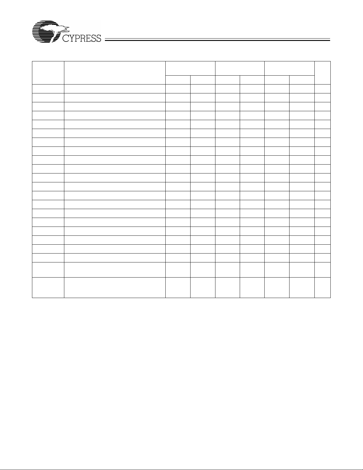
Selectio n Guide
7C4261/71/81/91V-10 7C4261/71/81/91V-15 7C4261/71/81/91V-25
Maximum Frequency (MHz) 100 66.7 40
Maximum Access Time (ns) 8 10 15
Minimum Cycle Time (ns) 10 15 25
Minimum Data or Enable Set-Up (ns) 3.5 4 6
Minimum Data or Enable Hold (ns) 0 0 1
Maximum Flag Delay (ns) 8 10 15
Active Power Supply
Current (I
Density 16k x 9 32k x 9 64k x 9 128k x 9
Package 32-pin PLCC 32-pin PLCC 32-pin PLCC 32-pin PLCC
CC1
) (mA)
Commercial 25 25 25
Industrial 30
CY7C4261V CY7C4271V CY7C4281V CY7C4291V
Maximum Ratings
(Abov e which the useful life may be impaired. For user guidelines, not tested.)
Storage Temperature .......................................−65
Ambient Temperature with
Po wer Applied....................................................−55
Supply Voltage to Ground Potential..................−0.5V to +3.6V
DC Voltage Applied to Outputs
in High Z State..............................................−0.5V to V
DC Input Voltage...........................................−0.5V to V
°
C to +150°C
°
C to +125°C
+0.5V
CC
+0.5V
CC
Output Current into Outputs (LOW)............................. 20 mA
Static Discharge Voltage .......... ............. ....................>2001V
(per MIL-STD-883, Method 3015)
Latch-Up Current.....................................................>200 mA
Operating Range
Ambient
Range
Commercial 0°C to +70°C 3.3V ±300 m V
Industrial
Temperature
−40°
C to +85°C 3.3V ±300 mV
[1]
V
CC
2
CY7C4261V/CY7C4271V
CY7C4281V/CY7C4291V
Pin Definitions
Signal Name Description I/O Description
D
0−8
Q
0−8
WEN1 Wr ite Enable 1 I The only write enable when device is configured to have programmable flags . Data is
WEN2/LD
Dual Mode Pin
REN1, REN2 Read Enable
WCLK Write Clock I The rising edge clocks data into the FIFO when WEN1 is LO W and WEN2/LD is HIGH
RCLK Read Clock I The rising edge clocks data out of the FIFO when REN 1 and REN2 are LOW and the FIFO
EF Empty Flag O When EF is LOW, the FIFO is empty. EF is synchronized to RCLK.
FF Full Flag O When FF is L OW, the FIFO is full . FF is synchronized to WCLK.
PAE Programmable
PAF Programmable
RS Reset I Resets device to empty condition. A reset is re quired before an init ial read or write
OE Output Enable I When OE is LOW , t he FIFO’s data outputs drive the bus to which they are connected. If OE is
Data Inputs I Data Inputs for 9-bit bus
Data Outputs O Data Outputs for 9-bit bus
written on a LOW-to-HIGH transition of WCLK when WEN1
If the FIFO is configured to have two write enables, data is written on a LOW-to-HIGH transition
of WCLK when WEN1
Wr ite Enable 2 I If HIGH at reset, thi s pin operates as a second write enable. If LOW at reset, this pin
Load
Inputs
Almost Empty
Almost Full
operates as a contro l to write or read the programmable flag offsets. WEN1
LOW and WEN2 must be HIGH to write data into the FIFO. Data will not be written into the FIFO
if the FF
is LOW . If the FIFO is configured to have programmable flags, WEN2/LD is held LOW
to write or read the programmable flag offsets.
I Enables the devi ce for Read operation. Both REN1 and REN2 must be asserted to
allow a read operation.
and the FIFO is not Full. When LD
offset register.
is not Empty. When WEN2/LD
register.
O When PAE is LOW, the FIFO is almost empty based on the almost empty offset value pro-
grammed into the FIFO. P AE
O When PAF is LOW, the FIFO is almost full based on the almost full offset value programmed
into the FIFO . P AF
operation after power-up.
HIGH , t he FI FO ’s outputs are in High Z (high-impedance) state.
is LOW and WEN2/LD and FF are HIGH.
is asserted, WCLK writes data into the programmable flag-
is LOW , RCLK reads data out of the programmable flag-offset
is synchronized to RCLK.
is synchronized to WCLK.
is asserted and FF is HIGH.
must be
3
CY7C4261V/CY7C4271V
CY7C4281V/CY7C4291V
Electrical Characteristics
Over the Operating Range
Parameter Description T est Conditions
V
OH
V
OL
V
IH
Output HIGH
Voltage
Output LOW
Voltage
Input HIG H
VCC = Min., IOH = −1.0 mA
V
= 3.0V , IOH = −2.0 mA
CC
VCC = Min., IOL = 4.0 mA
V
= 3.0V , IOL = 8.0 mA
CC
Voltage
V
IL
I
IX
I
OZL
I
OZH
[2]
I
CC1
[3]
I
SB
Capacitance
Input LOW
Voltage
Input Leakage
Current
Output OFF,
High Z Current
Active Power
Supply Current
Average Standby Current
[4]
V
= Max.
CC
OE > VIH,
V
< VO< V
SS
CC
Com’l 25 25 25 mA
Ind 30 mA
Com’l 4 4 4 mA
Ind 4 mA
Parameter Description Test Conditions Max. Unit
C
IN
C
OUT
Input Capacitance TA = 25°C, f = 1 MHz,
Output Capacitance 7 pF
AC Test Loads and Waveforms (-15 & -25)
7C4261/71/81/91V
-10
7C4261/71/81/91V
-15
7C4261/71/81/91V
-25
2.4 2.4 2.4 V
.04 0.4 0.4 V
2.0 V
−0.5
−10
−10
CC
0.8
+10
+10
2.0 V
−0.5
−10
−10
CC
0.8
+10
+10
2.0 V
−0.5
−10
−10
5 pF
V
= 3.3V
CC
[5, 6]
UnitMin. Max. Min. Max. Min. Max.
CC
0.8 V
+10
+10
V
µA
µA
C
L
R1=330Ω
200
Ω
R2=510
4281V–4
ALL INPUT PULSES
3.0V
Ω
GND
≤
3ns
90%
10%
90%
10%
≤
3
ns
4281V–5
3.3V
OUTPUT
INCLUDING
JIGA ND
SCOPE
Equivalent to: THÉ VENIN EQUIVALENT
OUTPUT 2.0V
AC Test Loads and Waveforms (-10)
VCC/2
50Ω
3.0V
I/O
Notes:
1. V
Range for commercial -10 ns is 3.3V ±150mV.
CC
2. Input signals switch from 0V to 3V with a rise/fall time of less than 3 ns, clocks and clock enables switch at maximum frequency of 20 MHz, while data inputs
switch a t 10 M Hz. Outputs a re unloaded.)
3. All inputs = V
4. Tested initially and after any design or process changes that may affect these parameters.
= 30 pF for all AC parameters except for t
5. C
L
6. C
= 5 pF f or t
L
Z0=50
Ω
− 0.2V, except WCLK and RCLK ( which ar e at frequenc y = 0 MHz). All o utputs are u nl oaded.
CC
.
OHZ
.
OHZ
GND
≤
3ns
ALL INPUT PULSES
90%
10%
90%
10%
4282V–5
3 ns
≤
4
CY7C4261V/CY7C4271V
CY7C4281V/CY7C4291V
Switching Characteristics
Over the Operating Range
Parameter Description
t
S
t
A
t
CLK
t
CLKH
t
CLKL
t
DS
t
DH
t
ENS
t
ENH
t
RS
t
RSS
t
RSR
t
RSF
t
OLZ
t
OE
t
OHZ
t
WFF
t
REF
t
PAF
t
PAE
t
SKEW1
Clock Cycle Frequency 100 66.7 40 MHz
Data Access Time 2 8 2 10 2 15 ns
Clock Cycle Time 10 15 25 ns
Clock HIGH Time 4.5 6 10 ns
Clo ck L OW Ti m e 4.5 6 10 ns
Data Set-Up Time 3.5 4 6 ns
Data Hold Time 0 0 1 ns
Enable Set-Up Time 3.5 4 6 ns
Enable Ho ld Time 0 0 1 ns
Reset Pulse Width
[7]
Reset Set-Up Time 8 10 15 ns
Reset Recovery Time 8 10 15 ns
Reset to Flag and Output Time 10 15 25 ns
Output En a ble to Output in L o w Z
Output En a ble to Output Valid 3 7 3 10 3 12 ns
Output Enable to Output in High Z
Write Clock to Full Flag 8 10 15 ns
Read Clock to Empty Flag 8 10 15 ns
Clo ck to Progra m m able Alm ost-Full Fl a g 8 10 15 ns
Clo ck to Progra m m able Alm ost-Full Fl a g 8 10 15 ns
Skew Time between Read Clock and
Write Clock for Empty Flag and Full Flag
t
SKEW2
Skew Time between Read Clock and
Write Clock for Almost-Empty Flag and
Almost-Full Flag
Notes:
7. Pulse widths less than minimum values are not allowed.
8. Values guaranteed by design, not currently tested.
7C4261/71/81/91V
-10
7C4261/71/81/91V
-15
7C4261/71/81/91V
-25
UnitMin. Max. Min. Max. Min. Max.
10 15 25 ns
[8]
[8]
0 0 0 ns
3 7 3 8 3 12 ns
5 6 10 ns
10 15 18 ns
5

Switching W aveforms
CY7C4261V/CY7C4271V
CY7C4281V/CY7C4291V
Write Cycle Timing
WCLK
D
0–D17
WEN1
WEN2
(if applic ab le)
FF
RCLK
REN1, REN2
Read Cycle Timing
RCLK
t
ENS
REN1, REN2
EF
t
SKEW1
t
ENH
t
CLKH
[9]
t
CLKH
t
WFF
t
REF
t
A
t
CLK
t
CKL
NO OPERATION
t
t
DS
t
CLKL
CLKL
t
ENS
t
DH
t
ENH
t
t
REF
NO OPERATION
NO OPERATION
WFF
4281V–6
Q
0–Q17
t
OLZ
OE
WCLK
WEN1
WEN2
Notes:
9. t
10. t
is the min imum t ime bet ween a rising RC LK edge and a r ising WCLK ed ge t o gua rantee that FF w ill go HIGH during the current clock cycle. If the time between the
SKEW1
rising edge of RCLK and the risin g edge of WCLK is less than t
is the minimum time between a rising WCLK edge and a rising RCLK edge to guarantee that EF will go HIGH during the current clock cycle. It the time between the
SKEW1
rising edge of W CLK and the rising e dge of RCLK is less than t
VALID DATA
t
t
OE
[10]
t
SKEW1
, then FF may no t c hange state unt il the ne x t WCLK risi ng edge.
SKEW1
, then EF ma y not chang e s tate until the ne xt RC LK ris ing edge .
SKEW2
OHZ
4281V–7
6

CY7C4261V/CY7C4271V
CY7C4281V/CY7C4291V
Switching W aveforms
Reset Timing
[11]
(continued)
t
RS
RS
t
RSR
REN1
t
RSS
,
REN2
t
RSS
t
RSR
WEN1
t
RSR
EN2/LD
[13]
t
RSF
t
RSS
EF,PAE
t
RSF
PAF
FF,
t
RSF
Q
Q
0
8
−
OE=1
[12]
OE=0
Notes:
11. The clocks (RCLK, WCLK) can be free-running during reset.
12. After reset, the outputs will be LOW if OE
13. Holding WEN2/LD HIGH during r eset w ill m ake t he pin ac t as a sec ond en able pin. Holdi ng WEN2/LD LOW during reset will make the pin act as a load enable for the
programmab le flag of fs et regi sters .
= 0 and three- state if O E=1.
4281V–8
7

CY7C4261V/CY7C4271V
CY7C4281V/CY7C4291V
Switching W aveforms
(continued)
First Data Word Latency after Reset with Read and Write
WCLK
t
DS
D0–D
8
WEN1
WEN2
(if applicable)
RCLK
EF
REN1,
REN2
Q
0–Q8
OE
t
ENS
D
(FIRST V ALID WRITE)
0
t
SKEW1
t
OLZ
t
FRL
[14]
D
t
REF
1
D
2
t
A
t
OE
D
3
[15]
t
A
D
0
D
4
D
1
Notes:
14. When t
The Latency Timing appl ies onl y at t he Empty B ound ary (EF
15. The first word is available the cycle after EF goes HIGH, alwa ys.
> minimum specifi cation, t
SKEW1
(maximum) = t
FRL
+ t
CLK
= LOW).
SKEW2
. When t
< minimum specification, t
SKEW1
(maximum) = ei ther 2*t
FRL
CLK
+ t
SKEW1
or t
4281V–9
+ t
CLK
SKEW1
.
8

CY7C4261V/CY7C4271V
CY7C4281V/CY7C4291V
Switching W aveforms
Empty Flag Timing
WCLK
t
DS
D0–D
8
WEN1
WEN2
(if applicable)
RCLK
EF
REN1,
REN2
OE
Q
0–Q8
LOW
DATA WRITE 1
t
ENS
t
ENS
(continued)
t
ENH
t
ENH
[14] [14]
t
FRL
t
SKEW1
DATA IN OUTPUT REGISTER
t
REF
t
DS
DATA WRITE 2
t
ENH
t
ENS
t
t
ENS
t
REF
t
A
ENH
t
SKEW2
t
FRL
t
REF
DATA READ
4281V–10
9

CY7C4261V/CY7C4271V
CY7C4281V/CY7C4291V
Switching W aveforms
Full Flag Timing
WCLK
[9]
t
SKEW1
D
0–D8
FF
WEN1
WEN2
(if applicable)
RCLK
t
REN1,
REN2
ENS
(continued)
NO WRITE
t
WFF
t
ENH
NO WRITE
t
DS
t
SKEW1
[9]
DATA WRITE
DATA WRITE
t
WFF
t
ENS
t
WFF
t
ENH
OE
Q0–Q
LOW
DATA IN OUTPUT REGISTER
8
t
A
DATA READ
t
A
NEXT DATA READ
4281V–11
10

CY7C4261V/CY7C4271V
CY7C4281V/CY7C4291V
Switching W aveforms
(continued)
Programmable Almost Empty Flag Timing
t
CLKH
WCLK
t
ENS
WEN1
WEN2
(if applic ab le)
t
ENS
PAE
[16]
t
SKEW2
RCLK
REN1,
REN2
Programmable Almost Full Flag Timing
t
CLKH
t
ENH
t
ENH
t
CLKL
t
CLKL
Note
t
PAE
Note
17
19
t
ENS
N + 1 WORDS
IN FIFO
t
t
ENH
ENS
Note18
t
PAE
4281V–12
WCLK
t
t
ENH
ENS
WEN1
WEN2
(if applicable)
PAF
t
t
ENH
ENS
FULL −(M+1)WORDS
IN FIFO
Note
20
t
PAF
FULL −MWORDS
t
SKEW2
IN FIFO
[22]
[21]
RCLK
t
ENS
t
ENS
t
ENH
REN1,
REN2
Notes:
16. t
17. PAE offset= n.
18. If a read is performed on this rising edge of the read clock, there will be Empty + (n−1) words in the FIFO when PAE goes LO W.
19. If a write is performed on this rising edge of the write clock, there will be Full − (m−1) words of the FIFO when PAF goes LOW.
20. PAF offset = m.
21. 16K − m words for CY7C4261V, 32K – m words for CY7C4271V, 64K − m words for CY7C4281V, and 128K − m words for CY4291V.
22. t
is the minimum time between a ris ing WCLK and a rising RCLK edge f or P AE to chang e state during that clock cycle. If the ti me between the edge of W CLK and the
SKEW2
rising RCLK is les s than t
is the minimum t ime betw een a risin g RCLK edge a nd a r ising WC LK edge for PAF to c hange during t hat c lock cycle. If the time between the rising edge of RCLK
SKEW2
and the rising edge o f W CLK is l ess than t
, then PAE may not change sta te unt il the ne x t R CLK.
SKEW2
, then PAF may not change state until th e ne x t WCLK.
SKEW2
t
PAF
4281V–13
11

CY7C4261V/CY7C4271V
CY7C4281V/CY7C4291V
Switching W aveforms
(continued)
WriteProgrammable Registers
t
CLKH
WCLK
WEN2/LD
WEN1
D
0–D8
Read Programmable Registers
t
CLKH
RCLK
WEN2/LD
t
CLK
t
CLK
t
ENS
t
ENS
t
ENS
t
DS
t
CLKL
PAE OFFSET
LSB
t
CLKL
t
ENH
t
ENH
t
DH
PAE OFFSET
MSB
PAF OFFSET
LSB
PAF OFFSET
MSB
4281V–14
t
ENS
REN1,
REN2
t
A
Q
0–Q15
UNKNOWN
Architecture
The CY7C4261/71/81/91V consists of an array of 16k, 32k,
64k, or128k words of 9 bits each (implemented by a dual-port
array of SRAM cells), a read pointer, a write pointer, control
signals (RCLK, WCLK, REN1
flags (EF
, PAE , PAF, FF ).
, REN2, WEN1, WEN2, RS), and
Resetting the FIFO
Upon power-up, the FIFO must be reset with a Reset (RS)
cycle. This causes the FIFO to enter the Empty condition signifi ed by EF
after the ris ing edge of RS. In order for the FIFO to reset to its
default stat e, th e user must not read or write whi le RS
All flags ar e guar anteed to b e vali d t
being LOW. All data outputs (Q
after RS is ta ken LO W .
RSF
) go LOW t
0−8
RSF
is LOW.
FIFO Operation
When the WEN1 signal is active LOW, WEN2 is active HIGH,
and FF
is activ e HIGH, data present on the D
pins is written
0−8
PAF OFFSET
MSB
PAE OFFSET LSB
PAE OFFSET MSB
PAF OFFSET
LSB
4281V–15
into the FIFO on each rising edge of the WCLK signal. Similarly, when the REN1
EF
is active HIGH, da ta in the FIFO m emory will be pre sented
on the Q
edge of RCLK while REN1
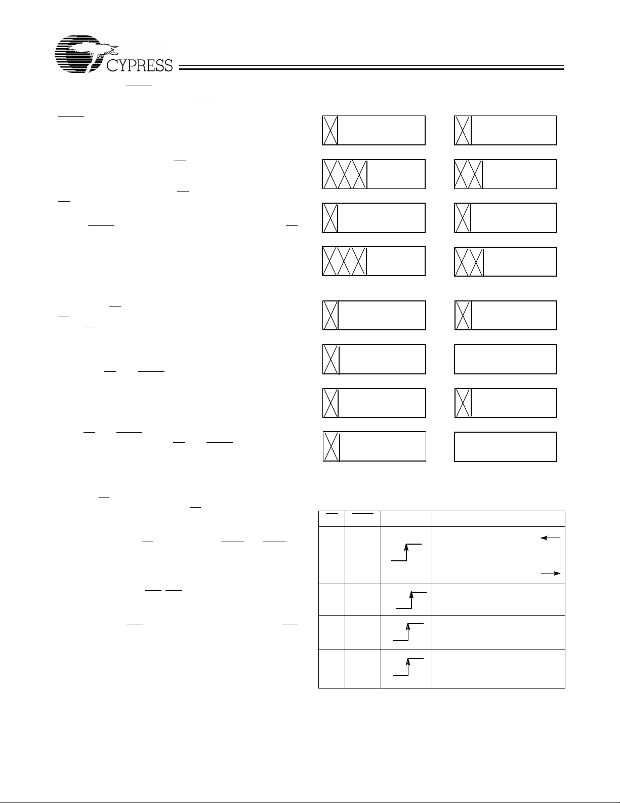
REN2
outputs. New data will be presente d on each risi ng
0−8
must set up t
funct ion. WEN1
it to be a valid write function.
An output enable (OE
and REN2 signals are active LOW and
and REN2 are active. REN1 and
and WEN2 must occur t
before WCLK for
ENS
before RCLK for it to be a valid read
ENS
) pin is provided to three-state the Q
outputs when OE is asserted. When OE is enabled (LOW),
data in the output regist er will be available to the Q
after t
output data on the FIFO that is read enabled.
. If devices are cascaded, the OE function will only
OE
0−8
outputs
The FIFO contains overflow circuitry to disallow additional
writes when the FIFO is full, and und erflow circ uitry to disallow
additional reads when the FIFO is empty. An empty FIFO
maintains the data of the last valid read on its Q
even after additional reads occur.
outputs
0−8
0−8
12
CY7C4261V/CY7C4271V
64k x 9
8
0
8
0
8
0
Empty Offset(LSB) Reg.
Default Value = 007h
FullOffset(LSB) Reg
Default Value = 007h
(MSB)
7
7
7
8
0
8
0
8
0
8
0
Empty Offset (LSB) Reg.
Default Value = 007h
FullOffset (LSB) Reg
Default Value = 007h
(MSB)
(MSB)
7
7
4281V–16
128kx 9
8
0
(MSB)
7
Default Value= 000h
Default Value= 000h
Default Value= 000h
Default Value= 000h
16k x 9
8
0
8
0
8
0
Empty Offset (LSB) Reg.
DefaultValue = 007h
FullOffset(LSB)Reg
DefaultValue = 007h
(MSB)
7
5
7
8
0
8
0
8
0
0
Empty Offset (LSB) Reg.
DefaultValue = 007h
FullOffset(LSB)Reg
DefaultValue = 007h
(MSB)
(MSB)
7
7
32k x 9
0
(MSB)
Default Value = 000h
DefaultValue = 000h
Default Value= 000h
DefaultValue = 000h
6
8
5
8
6
Empty Offset (LSB)
Empty Offset (MSB)
Full Offset (LSB)
Full Offset (MSB)
CY7C4281V/CY7C4291V
Write Enable 1 (WEN1
grammable flags, Write Enable 1 (WEN1
)
- If the FIFO is configured for pro) is the only wri te en-
able control pin. In this configuration, when Write Enable 1
(WEN1
) is LOW, data can be l oade d int o the i nput r egist er an d
RAM array on t he LO W-to-HIGH transition of e very write c lock
(WCLK). Data is stored is the RAM array sequentially and independently of any on-going read operation.
Write Enable 2 /Load (WEN2/LD
)
- This is a dual-purpose pin.
The FIFO is configured at Reset to have programmable flags
or to ha ve two write ena bles, which al lows f or dept h e xpansion.
If Write Enab le 2/Load (WEN2/ LD
(RS
=LOW), this pin operates as a second write enable pin.
) is set active HIGH at Reset
If the FIFO is configure d to hav e two write enables , when Writ e
Enable (WEN1
) is LOW and Write Enable 2/Load (WEN2/LD )
is HIGH, data can be loaded into the input register and RAM
array on the LOW-to-HIGH transition of every write clock
(WCLK). Data is stored in the RAM array sequentially and independently of any on-going read operation.
Programming
When WEN2/LD is held L O W duri ng Reset , thi s pin is t he loa d
(LD
) enable for flag offset programming. In this configuration,
WEN2/LD
contained in the CY7C4261/71/81/91V for writing or reading
data to these registers.
When the device is configured for programmable flags and
both WEN2/LD
transit ion of WCLK writes data from the data inputs to the empty offset least significant bit (LSB) register. The second, third,
and fourth LOW -t o-HIGH transit ions of WCLK store data in the
empty offset most signi fic ant bit (MSB) reg ister, full offset LSB
register, and full offset MSB register, respectively, when
WEN2/LD
sition of WCLK while WEN2/LD
data to the empty LSB regi ster again. Figur e 1 sh ows the registers sizes and default values for the various device types.
It is not ne cessary to write to al l the of fset regist ers at o ne time.
A subset of the of fset regist ers can be written; then by bringin g
the WEN2/LD
write operation. The next time WEN2/LD
eration stores data in the next offset register in sequence.
The contents of the offset registers can be read to the data
outputs when WEN2/LD
LOW . LOW-to-HIGH transitions of RCLK read register contents to the
data outputs. Writes and reads should not be pe rformed simultaneously on the offset registers.
Programmable Flag (PAE
Whether the flag offset registers are programmed as described in Table 1 or the default val ues are used, the programmable
almost-empty flag (PAE
states are determined by their corresponding offset registers and the
difference between the read and write pointers.
can be used to access th e fo ur 9- bit of fset regi sters
and WEN1 are LOW, the first LOW-to-HIGH
and WEN1 are LOW. The fifth LOW-to-HIGH tran-
and WEN1 are LOW writes
input HIGH, the FIFO is returned to normal read and
is brought LOW, a write op-
is LOW and both R EN1 and REN2 are
, P AF ) Operation
) and programmable almost-full flag (PAF)
Figure 1. Offset Register Locati on and Default Val ues
T able 1. Writing the Offset Registers
LD WEN WCLK
[24]
Selection
0 0
0 1 No Oper ati on
1 0 Write Into FIFO
1 1 No Oper ati on
13

CY7C4261V/CY7C4271V
CY7C4281V/CY7C4291V
The number for med by the empty offset least significant bit
register and empty offset most significant bit register is referred to as n and determines the operation of P AE
. P AF is synchronized to the LOW-to-HIGH transition of RCLK by one flip-flop and is
LOW when the FIFO contains n or fewer unread words. PAE
is set
HIGH by the LOW-to-HIGH transition of RCLK when the FIFO contains (n+1) or greater unread words.
The number formed by the full offset least signif icant bit regis ter and full offset most significant bit register is referred to as
m and determines the operation of PAF
. PAE is synchronized to the
LOW-to-HIGH transition of WCLK by one flip-flop and i s set LOW
when the number of unread words in the FIFO is greater than or equal
to CY7C4261V (16 k − m), CY7C4271V (32k − m), CY7C4281V
(64k − m) and CY7C4291V (128k − m). P AF
is set HIGH by the LOWto-HIGH transition of WCLK when the number of available memory
locations is greater than m.
Table 2. Status Flags
Number of W ords in FIFO
FF PAF PAE EFCY7C4261V CY7C4271V CY7C4281V CY7C4291V
0 0 0 0 H H L L
[24]
1 to n
(n+1) to (1638 − (m+1)) (n+1) to (32768 −
(16384 − m)
[25]
to 16383 (32768 − m)
1 to n
(m+1))
[24]
1 to n
(n+1) to (65536 −
(m+1))
[25]
to 32767 (65536 − m)
[24]
[24]
1 to n
(n+1) to (131072−
(m+1))
[25]
to 65535 (131072 − m)
[25]
to
H H L H
H H H H
H L H H
131071
16384 32768 65536 131072 L L H H
Notes:
23. The same selection sequence applies to reading from the registers. REN1
24. n = Empty Offset (n=7 default value).
25. m = Full Offset (m=7 default value).
Width Expansion Configuration
and REN2 are enabl ed and a r ead is perf ormed on the LOW - to-HIG H tr ansi tion of RCLK
Flag Ope r ati o n
Word width may be increased simply by connecti ng the corresponding input controls signal s of multiple de vices . A composite flag s houl d b e creat ed for each of the end- point stat us fl ags
(EF
and FF). The partial status flags (P AE and PAF) can be detected
from any one device. Figure 2 demonstrates a 18-bit word width by
using two CY7C42x1Vs. Any word width can be attained by adding
additional CY7C42x1Vs.
When the CY7C4 2x1V is in a Width Expansion Co nfi guration,
the Read Enable (REN2
ure 2). In this configuration, the Write Enable 2/Load (WEN2/LD
) control input can be grounded (See Fig-
) pin
is set to LOW at Reset so that the pin operates as a control to load
and read the programmable flag offsets.
The CY7C4261/71/81/91V de vice s pro vide fiv e flag pi ns to indicate the c ondition of the FIFO co ntents. Empty, Full, PA E
PAF
are synchronous.
, and
Full Flag
The Full Flag (FF
tions are inhibited whenever FF
WEN1
and WEN2/LD. FF is synchronized to WCLK, i.e., it is exclu-
) will go LOW when the device is full. Write opera-
is LOW regardless of the state of
sively updated by each rising edge of WCLK.
Empty Flag
The Empty Flag (EF
operations are inhibited whenever EF
of REN1
and REN2. EF is synchronized to RCLK, i.e., it is e xclusively
) will go LOW when the device is empty. Read
is LOW , regardless of the state
updated by each rising edge of RCLK.
14

CY7C4261V/CY7C4271V
CY7C4281V/CY7C4291V
RESET
DATAIN (D)
WRITECLOCK(WCLK)
WRITE ENABLE1(WEN1
WRITE ENABLE2/LOAD
(WEN2/LD
918
)
CY7C4261V
)
CY7C4271V
PROGRAMMABLE(PAF
FULLFLAG(FF
FULLFLAG(FF
Figure 2. Block Diagram of 16k/32k/64k/128k x 9 Low Voltage Deep Sync FIFO Memory Used in a Width Expansion
)# 1
)# 2
CY7C4281V
)
CY7C4291V
FF
ReadEnable2 (REN2)
(RS)
EF
9
Configuration
RESET(RS)
9
CY7C4261V
CY7C4271V
CY7C4281V
CY7C4291V
FF
Read Enable 2 ( REN2
READCLOCK(RCLK)
READENABLE1 (REN1
OUTPUT ENABLE(OE
PROGRAMMABLE(PAE
EMPTY FLAG (EF
EMPTY F LAG (EF
EF
DATA OUT (Q)
918
)
)#1
)#2
4281V–17
)
)
)
Ordering Information
16Kx9 Low Voltage Deep Sync FIFO
Speed
(ns) Ordering Code
10 CY7C4261V-10JC J65 32-Lead Plastic Leaded Chi p Carri er Commercial
15 CY7C4261V-15JC J65 32-Lead Plastic Leaded Chi p Carri er Commercial
CY7C4261V-15JI J65 32-Lead Plastic Leaded Chip Carrier Industrial
25 CY7C4261V-25JC J65 32-Lead Plastic Leaded Chi p Carri er Commercial
Package
Name
Package
Type
Operating
Range
32Kx9 Low Voltage Deep Sync FIFO
Speed
(ns)
10 CY7C4271V-10JC J65 32-Lead Plastic Leaded Chi p Carri er Commercial
15 CY7C4271V-15JC J65 32-Lead Plastic Leaded Chi p Carri er Commercial
25 CY7C4271V-25JC J65 32-Lead Plastic Leaded Chi p Carri er Commercial
64kx9 Low Voltage Deep Sync FIFO
Speed
(ns)
10 CY7C4281V-10JC J65 32-Lead Plastic Leaded Chi p Carri er Commercial
15 CY7C4281V-15JC J65 32-Lead Plastic Leaded Chi p Carri er Commercial
25 CY7C4281V-25JC J65 32-Lead Plastic Leaded Chi p Carri er Commercial
Orde ring Co de
CY7C4271V-15JI J65 32-Lead Plastic Leaded Chip Carrier Industrial
Orde ring Co de
CY7C4281V-15JI J65 32-Lead Plastic Leaded Chip Carrier Industrial
Package
Name
Package
Name
Package
Type
Package
Type
15
Operating
Range
Operating
Range

CY7C4261V/CY7C4271V
CY7C4281V/CY7C4291V
Ordering Information
128kx9 Low Voltage Deep Sync FIFO
Speed
(ns)
Orde ring Co de
10 CY7C4291V-10JC J65 32-Lead Plastic Leaded Chi p Carri er Commercial
15 CY7C4291V-15JC J65 32-Lead Plastic Leaded Chi p Carri er Commercial
CY7C4291V-15JI J65 32-Lead Plastic Leaded Chip Carrier Industrial
25 CY7C4291V-25JC J65 32-Lead Plastic Leaded Chi p Carri er Commercial
Document #: 38-00656-B
Package Diagram
Package
Name
Package
Type
32-Lead Plastic Leaded Chip Carrier J65
Operating
Range
51-85002-B
© Cypress Semiconductor Corporation, 1999. The information contained herein is subject to change without notice. Cypress Semiconductor Corporation assumes no responsibility for the use
of any circuitry other than circuitry embodied in a Cypress Semiconductor product. Nor does it con vey or imply any lice nse under patent or other rights. Cypress Semicondu ctor does not authorize
its products for use as critical components in life-support systems where a malfunction or failure may reasonably be expected to result in significant injury to the user. The inclusion of Cypress
Semiconductor products in life-support systems application implies that the manufacturer assumes all risk of such use and in doing so indemnifies Cypress Semiconductor against all charges.
 Loading...