

Cypress Semiconductor CY7C4292V-25ASC, CY7C4292V-15ASC, CY7C4292V-10ASC, CY7C4282V-25ASC, CY7C4282V-15ASC Datasheet
...
Features
CY7C4282V
CY7C4292V
64K/128Kx9 Lo w Voltage Deep Sync FIFOs
w/ Retransmit & Depth Expansion
Functional Description
• 3.3V operation for low power consumption and easy
integration into low-voltage systems
• High-speed, low-power, first-in fir st- out (FIFO)
memories
• 64K x 9 (CY7C4282V)
• 128K x 9 (CY7C4292V)
• 0.35 micron CMOS for optimum speed/power
• High-speed, Near Zero Latency (True Dual- Ported
Memory Cell), 100-MH z operation (10 ns read/write
cycle times)
• Low po w er
I
= 25 mA
—
CC
I
= 6 mA
—
SB
• Fully asynchronous and simultaneous read and write
operation
• Empty, Full, and Progra mmable Almost Empty and Almost Full status flags
• Retransmit function
Output Enable (OE
•
pin
)
• Independent read and write enable pins
• Supports free-running 50% duty cycle clock inputs
• Width Expansion Capabilit y
• Depth Expansion Capabil it y through token-passing
scheme (no ext ernal logic required)
• 64-pin 10x10 STQFP
• Pin-compatible 3.3V solution for CY7C4282/92
D
0−8
Logic
Block
Diagram
INPUT
REGISTER
The CY7C4282V/92V are hig h-speed, low-power, first-in first out (FIFO) memories with clocked read and write interfaces.
All devices are 9 bits wide. The CY7C4282V/92V can be cascaded to increase FI FO depth. Programmab le featur es include
Al m ost F u l l / A l m o s t E m pty f l a g s . These FIFOs provide solutions
for a wide variety of data buffering needs, including high-speed data
acquisition, multiprocessor interfaces, video and communications
buffering.
These FIFOs have 9-bit input and output ports that are controlled by separate clock and enable signals. The input port is
controlled by a f ree-runni ng cloc k (WCLK) and a Write Enab le
pin (WEN
).
Retransmit and Synchronous Almost Full/Almost Empty flag
features are available on these devices.
Depth expansi on is possi ble usi ng the Cascade I nput (XI
cade Output (XO
to the XI
should be connected to the XI
first de v ice is tied to V
should be tied to V
When WEN
rising edge of the WCLK signal. While WEN
), and First Load (FL) pi ns. T he XO pin is connected
pin of the next device, and the XO pin of the last device
pin of the first device. The FL pin of the
and the FL pin of all the remaining devices
SS
CC
is asserted, data is written into the FIFO on the
is held activ e, dat a
), Cas-
is continually written into the FIFO on each cycle. The output
port is controlled in a similar manner by a free-running Read
Clock (RCLK) and a Read Enable pin (REN
CY7C4282V/92V have an Output Enable pin (OE
). In addition, the
). The read
and write clocks ma y be tied together for single- clock opera tion
or the two cloc ks may be run independently for asynchron ous
read/write applications. Clock frequencies up to 67 MHz are
achievable.
WENWCLK
WRITE
CONTROL
WRITE
POINTER
RS
FL/RT
XI/LD
PAF/XO
RESET
LOGIC
EXPANSION
LOGIC
Cypress Semiconductor Corporation
FLAG
PROGRAM
REGISTER
FF
EF
PAE
PAF/XO
4282V–1
Dual Port
RAM Array
64Kx 9
128Kx
9
THREE-STATE
OUTPUT REGISTER
Q
0−8
OE
FLAG
LOGIC
READ
POINTER
READ
CONTROL
RCLK
REN
• 3901 North First Street • San Jose • CA 95134 • 408-943-2600
October 18, 1999
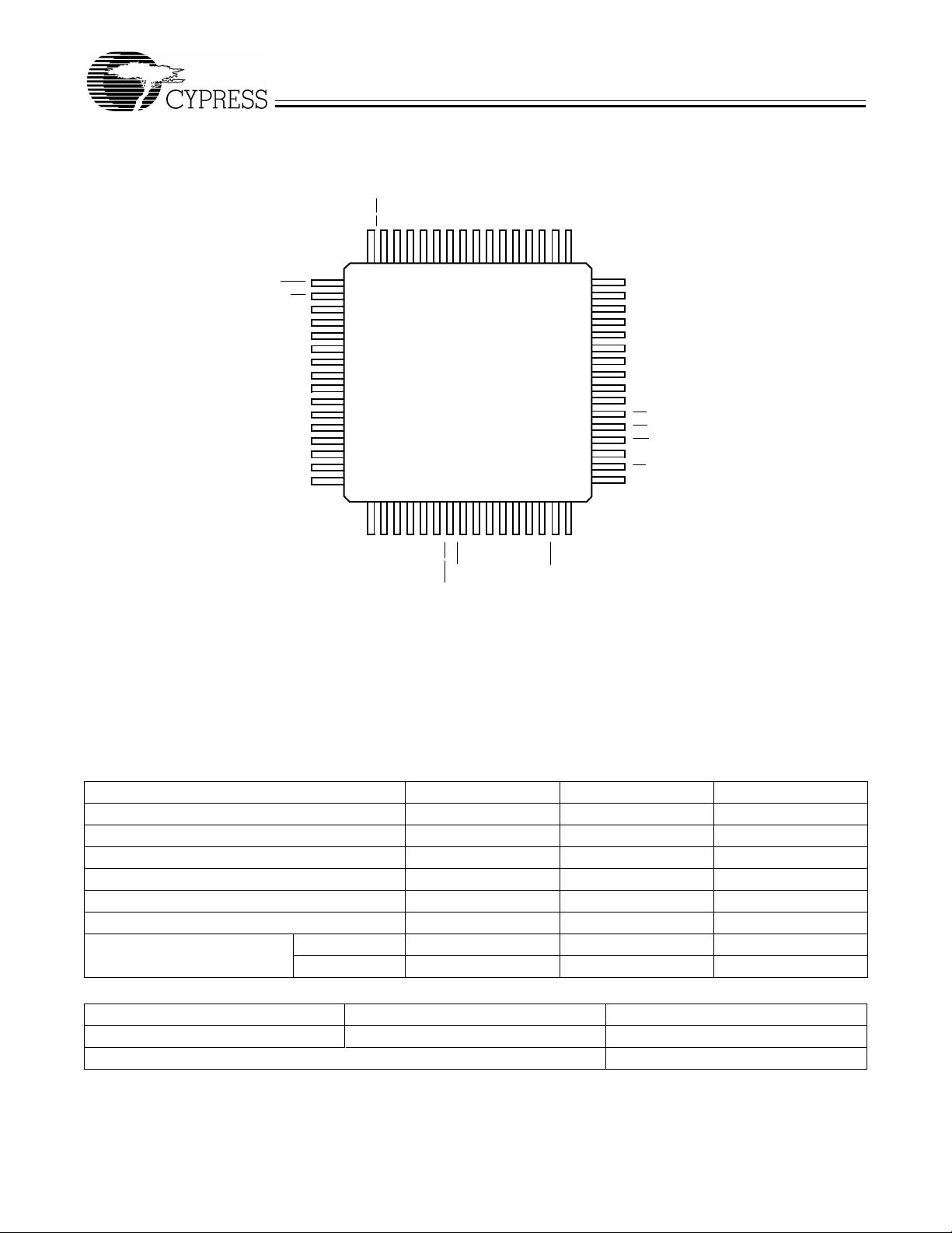
Pin Configuration
WEN
RS
D
D
D
N/C
N/C
N/C
N/C
N/C
N/C
N/C
D
D
D
D
CY7C4282V
CY7C4292V
STQFP
Top View
/LD
WCLK
XI
GND
N/C
N/C
N/C
N/C
N/C
1
2
8
7
6
5
4
3
2
3
4
5
6
7
8
9
10
11
12
13
14
15
16
17641863196220612160225923582457255626552754285329523051315032
CY7C4282V
CY7C4292V
VCCN/C
N/C
8
6
Q7Q
N/C
GND
Q
49
48
47
46
45
44
43
42
41
40
39
38
37
36
35
34
33
Q
5
Q
4
GND
Q
3
Q
2
V
CC
Q
1
Q
0
GND
N/C
FF
EF
OE
GND
FL
N/C
/RT
4282V–2
RCLK
Functional Description
(continued)
D1D
0
N/C
N/C
N/C
CC
N/C
N/C
N/C
N/C
V
PAE
PAF/XO
N/C
REN
GND
entering or exiting the Empty and Almost Empty states, the
flags are u pdated e xclus iv ely by th e RCLK. T he f lags deno ting
The CY7C4282V/92V provides four status pins: Empty, Full,
Programmab le Almost Empty, and Programmable Almost Full.
The Almost Em pty/Almost Full flags are programmable to single word granularity. The programmable flags default to Empty+7 and Full−7.
The flags are synchronous, i.e., they change state relative to
Almost Full, and Ful l st ates ar e upd ated e x clusi vel y b y WCL K.
The synchronous flag architecture guarantees that the flags
maintain their status for at least one cycle
All configurations are fabricated using an advanced 0.35µ
CMOS technology. Input ESD protection is greater than
2001V, and latch-up is prevented by the use of guard rings.
either the read cl ock (RCLK) or t he write cloc k ( WCLK). When
Selection Guide
7C4282V/92V-10 7C4282V/92V-15 7C4282V/92V-25
Maximum Frequency (MHz) 100 66.7 40
Maximum Access Time (ns) 8 10 15
Minimum Cycle Time (ns) 10 15 25
Minimum Data or Enable Set-Up (ns) 3.5 4 6
Minimum Data or Enable Hold (ns) 0 0 1
Maximum Flag Delay (ns) 8 10 15
Active Power Supply
Current (I
CC
) (mA)
Commercial 25 25 25
Industrial 30
CY7C4282V CY7C4292V
Density 64k x 9 128k x 9
Package 64-pi n 10x10 TQFP 64-pin 10x10 TQFP
2

CY7C4282V
CY7C4292V
Pin Definitions
Signal Name Description I/O Description
D
0−8
Q
0−8
WEN Wr ite Enabl e I The only write enable when device is configured to have programmable flags. Data is
REN Read Enable I Enables the devi ce for Read operation. REN must be asserted LOW to allow a Read
WCLK Write Clock I The rising edge cloc ks data into the FIFO when WEN is LOW and the FIFO is not Full.
RCLK Read Clock I The rising edge cloc k s d ata out of the FIFO whe n R EN is LOW and the FIFO is not Empty.
EF Empty Flag O When EF is LOW, the FIFO is empty. EF is synchronized to RCLK.
FF Full Flag O When FF is LOW, the FIFO is full. FF is synchronized to WCLK.
PAE Programmable
PAF/XO Programmable
FL/RT First Load/
XI/LD Expansion In-
OE Output Enable I When OE is LOW, the FIFO’s data out pu ts driv e t he bu s t o which the y ar e co nnect-
RS Reset I Resets device t o emp ty condition. A reset is re quired before an initial read or write
Data Inputs I Data Inputs for 9-bit bus.
Data Outputs O Data Outputs for 9-bit bus.
written on a LOW-to-HIGH transition of WCLK when WEN
operation.
When LD
When LD
is asserted, WCLK writes data into the programmable flag-offset register.
is LOW, RCLK reads data out of the programmable flag-offset register.
O When PAE is LOW, the FIFO is almost empty based on the almost empty offset value pro-
Almost Empty
grammed into the FIFO. P AE
O Dual-Mode Pin:
Almost Full/
Expansion
Output
Cascaded - Connected to XI
Not Cascaded - When PAF
programmed into the FIFO. PAF
I Dual-Mode Pin:
Retransmit
Cascaded - The first device in the daisy chain will have FL
will have FL
tied to VCC. In standard mode or width expansion, FL is tied to V
on all devices.
Not Cascaded - Retran sm it function is avail able in s t a n d-alone mode by strobing
RT.
I Dual-Mode Pin:
put/Load
Cascaded - Connected to XO
Not Cascaded - LD
is used to write or read the pr ogram mab le flag of f set regist ers. LD
must be as serted LOW during reset to en able standa lone or width expansi on operation.
If programmable offset regi ster access is not requi red, LD
ed. If OE
is HIGH , the FIFO ’s outputs are in High Z (high-impedance) state.
operation after power-up.
is asserted and FF is HIGH.
is synchronized to RCLK.
of next device.
is LOW, the FIFO is almost full based on the almost full offset value
is synchronized to WCLK.
tied to VSS; all othe r device s
of previous device.
can be tied to RS directly.
SS
Maximum Ratings
(Abov e which the useful life may be impaired. For user guidelines, not tested.)
Storage Temperature .......................................−65
Ambient Temperature with
Po wer Applied.................................................... −55
Supply Voltage to Ground Potential..........−0.5V to V
DC Voltage Applied to Outputs
in High Z State..............................................−0.5V to V
DC Input Voltage.........................................−0.5V to V
Output C ur re n t in to O u tp u ts (LOW) ..... ......... ... .. ..........20 m A
°
C to +150°C
°
C to +125°C
+0.5V
CC
+0.5V
CC
+0.5V
CC
Static Discharge Voltage ......................... ............ .. ....>2001V
(per MIL-STD-883, Method 3015)
Latch-Up Current .....................................................>200 mA
Operating Range
Range
Temperature V
Commercial 0°C to +70°C 3.3V + /−300mV
Ambient
Industrial
Notes:
1. T
2. VCC Range for commercial -10 ns is 3.3V ± 150 mV.
[1]
is the “ins tant on” ca se temper at ure.
A
−40°
C to +85°C 3.3V + /−300mV
3
CC
[2]
CY7C4282V
CY7C4292V
Electrical Characteristics
Over the Operating Range
Parameter Description Test Conditions
V
V
V
V
I
IX
I
OZL
I
OZH
I
CC1
OH
OL
IH
IL
[3]
Output HIGH Voltage VCC = Min., IOH = −1.0 mA
V
= 3.0V , IOH = −2.0 mA
CC
Output LOW Voltage VCC = Min., IOL = 4.0 mA
V
= 3.0V , IOL = 8.0 mA
CC
Input HIG H Voltage 2.0 V
Input LOW Voltage
Input Leakage Current V
Output O F F, High Z
= Max.
CC
OE > VIH, VSS < VO < V
Current
Active Power Supply
Current
[4]
I
SB
Average Standby
Current
Capacitance
[5]
Parameter Description Test Conditions Max. Unit
C
C
IN
OUT
Input Capacitance TA = 25°C, f = 1 MHz,
Output Capacitance 7 pF
7C4282V/92V
-10
7C4282V/92V
-15
7C4282V/92V
-25
UnitMin. Max. Min. Max. Min. Max.
2.4 2.4 2.4 V
0.4 0.4 0.4 V
CC
−0.5
−10
−10
CC
0.8
+10
+10
2.0 V
−0.5
−10
−10
CC
0.8
+10
+10
2.0 V
−0.5
−10
−10
CC
0.8 V
+10
+10
V
µA
µA
Com’l 25 25 25 mA
Ind 30 mA
Com’l 6 6 6 mA
Ind 6 mA
5 pF
V
= 3.3V
CC
Ω
4282V–4
[6, 7]
3.0V
GND
≤
3ns
ALL INPUT PULSES
90%
10%
90%
10%
≤
3
ns
4282V–5
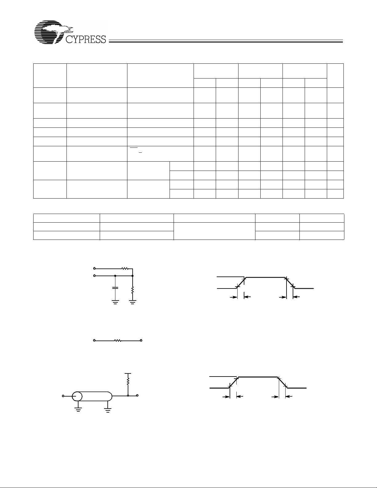
AC Test Loads and Waveforms (-15 , -25)
C
L
R1=330Ω
200
Ω
R2=510
3.3V
OUTPUT
INCLUDING
JIGA ND
SCOPE
Equivalent to: T HÉ VENIN EQUIVALENT
OUTPUT 2.0V
AC Test Loads and Waveforms (-10)
VCC/2
3.0V
50Ω
GND
3ns
I/O
Notes:
3. Input signals switch from 0V to 3V with a rise/fall time of less than 3 ns, clocks and clock enables switch at maximum frequency 20 MHz, while data inputs
switch a t 10 M Hz. Outputs are unloaded.
4. All inputs = V
5. Tested initially and after any design or process changes that may affect these parameters.
= 30 pF for all AC parameters except for t
6. C
L
7. C
= 5 pF f or t
L
Z0=50
Ω
− 0.2V, e xcept WCLK and RCLK (whic h a re s witching at fr equen cy = 0 MH z). Al l out puts ar e unload ed.
CC
.
OHZ
.
OHZ
≤
ALL INPUT PULSES
90%
10%
90%
10%
≤
3
ns
4282V–5
4
CY7C4282V
CY7C4292V
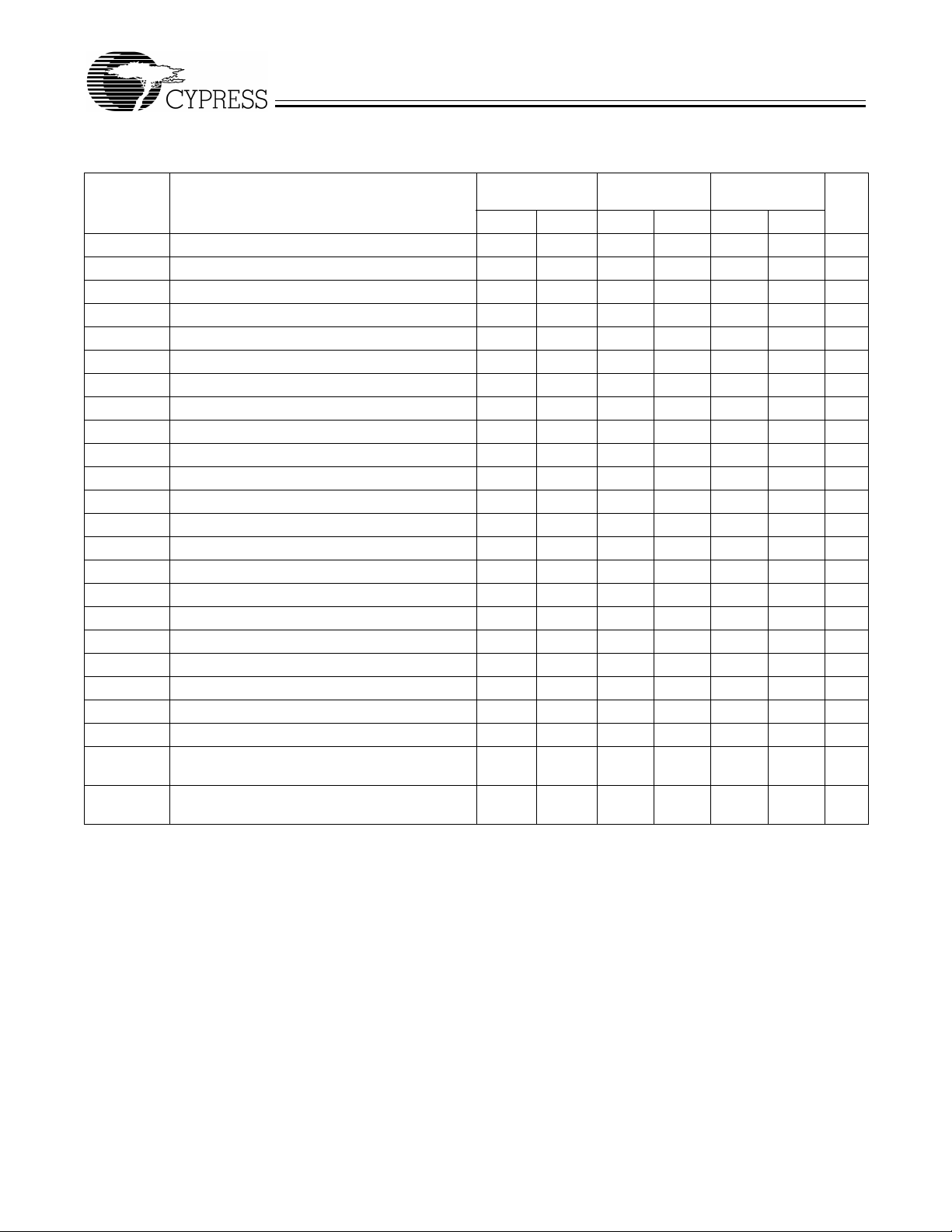
Switching Characteristics
Over the Operating Range
Parameter Description
t
S
t
A
t
CLK
t
CLKH
t
CLKL
t
DS
t
DH
t
ENS
t
ENH
t
RS
t
RSS
t
RSR
t
RSF
t
PRT
t
RTR
t
OLZ
t
OE
t
OHZ
t
WFF
t
REF
t
PAF
t
PAE
t
SKEW1
t
SKEW2
Notes:
8. Pulse widths less than minimum values are not allowed.
9. Values guaranteed by design, not currently tested.
Clock Cycle Frequency 100 66.7 40 MHz
Data Access Time 2 8 2 10 2 15 ns
Clock Cycle Time 10 15 25 ns
Clock HIGH Time 4.5 6 10 ns
Clock LOW Time 4.5 6 10 ns
Data Set-Up Time 3.5 4 6 ns
Data Hold Time 0 0 1 ns
Enable Set-Up Time 3.5 4 6 ns
Enable Hold Time 0 0 1 ns
Reset Pulse Width
[8]
Reset Set-Up Time 8 10 15 ns
Reset Recovery Time 8 10 15 ns
Reset to Flag and Output Time 10 15 25 ns
Retransmit Pulse Width 60 60 60 ns
Retransmit Recovery Time 90 90 90 ns
Output Enable to Output in Low Z
Output Enable to Output Valid 3 7 3 10 3 12 ns
Output Enable to Output in High Z
Write Clock to Full Flag 8 10 15 ns
Read Clock to Empty Flag 8 10 15 ns
Clock to Prog rammable Almost-Full Flag 8 10 15 ns
Clock to Prog rammable Almost-Full Flag 8 10 15 ns
Skew Tim e between Read Clock and Write Cl ock
for Empty Fl ag and Full Flag
Skew Tim e between Read Clock and Write Cl ock
for Almost -Empty Flag and Almost-Full Fl ag
[9]
7C4282V/92V
-10
7C4282V/92V
-15
7C4282V/92V
-25
UnitMin. Max. Min. Max. Min. Max.
10 15 25 ns
0 0 0 ns
[9]
3 7 3 8 3 12 ns
5 6 10 ns
10 15 18 ns
5
 Loading...