

Cypress Semiconductor CY7C4265-25AC, CY7C4265-15AC, CY7C4265-10AC, CY7C4255-25AC, CY7C4255-15AC Datasheet
...
8K/16K x 18 Deep Sync FIFOs
CY7C4255
CY7C4265
Cypress Semiconductor Corporation
• 3901 North First Street • San Jose • CA 95134 • 408-943-2600
April 21, 2000
Features
• High-speed, low-power, first-in fir st-out (FIFO)
memories
• 8K x 18 (CY7C4255)
• 16K x 18 (CY7C4265)
• 0.5 micron CMOS for optimum speed/power
• High-speed 100-MHz operation (10 ns read/writ e cycle
times)
• Low power — I
CC
= 45 mA
• Fully asynchr onous and simultaneous read and write
operation
• Empty , Full, Half Full, and pr ogrammable Almost Empty
and Almost Full status flags
• TTL compatible
• Retransmit function
• Output Enable (OE
)
pins
• Independent read and write enable pins
• Center power and ground pins for reduced noise
• Supports free-running 50% duty cycle clock inputs
• Width Expansion Capabilit y
• Depth Expansion Capability
• 64-pin PLCC, 64-pin TQFP and 64-pin STQFP
• Pin-compatible density upgrade to CY7C42X5 family
• Pin-compatible density upgrade to
IDT72205/15/25/35/45
Functional Description
The CY7C4255/65 are high-speed, low-power, f irst-in firs t-out
(FIFO) memories with clocked read and write interfaces. All
are 18 bits wide and are pin/functionally compatible to the
CY7C42X5 Synchronous FIFO fami ly. The CY7C4255/65 can
be cascaded to inc rease FIFO depth. Programmable features
include Almost Full/Almost Empty flags. These FIFOs provide
solutions for a wide variety of data buffering needs, including
high-speed data acquisition, multiprocessor interfaces, and communications buffering.
These FIFOs have 18-bit input and output ports that are controlled by separate clock and enabl e signals. The input port is
controlled by a Free-Running Clock (WCLK) and a Write Enable pin (WEN
).
When WEN
is asserted, data is written into the FIFO on the r isi ng
edge of the WCLK signal. While WEN
is held active, data is continually written into the FIFO on each cycle. The output port is controlled
in a similar manner by a free-running Read Clock (RCLK) and a Read
Enable pin (REN
). In addition, the C Y 7 C 4255/65 have an Output
Enable pin (OE
). The read and write clocks may be tied together for
single-clock operation or the two clocks may be run independently for
asynchronous read/wr ite applications. Clock frequencies up to 100
MHz are achievable.
Retransmit and Synchronous Almost Full/Almost Empty flag
features are available on these de vices.
Depth expansion is possibl e using the Cascade Input (WXI
,
RXI
), Cascade Output (WXO, RXO), and First Load (FL) pins. The
WXO
and RXO pins are connected to the WXI and RXI pins of the
next device, and the WXO
and RXO pins of the last device should be
connected to the WXI
and RXI pins of the first de vice. The FL pin of
the first device is tied to V
SS
and the FL pin of all the remaining devic-
es should be ti ed to V
CC
.
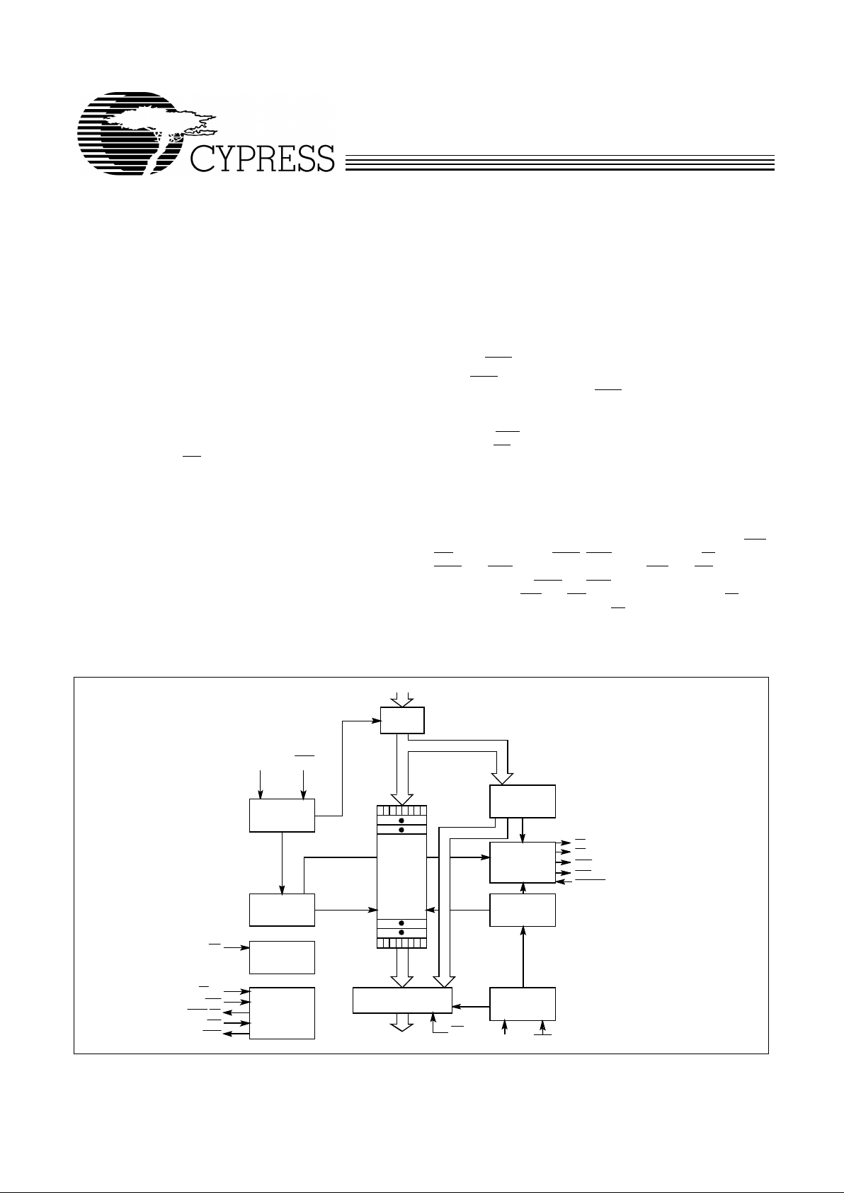
Q
0– 17
4255–1
THREE–STATE
OUTPUTREGISTER
READ
CONTROL
FLAG
LOGIC
WRITE
CONTROL
WRITE
POINTER
READ
POINTER
RESET
LOGIC
EXPANSION
LOGIC
INPUT
REGISTER
FLAG
PROGRAM
REGISTER
D
0– 17
REN
RCLK
FF
EF
PAE
WENWCLK
RS
FL/RT
WXI
OE
RAM
ARRAY
8Kx 18
16K x
18
PAF
WXO/HF
RXI
RXO
SMODE
Logic Block Diagram
CY7C4255
CY7C4265
2
Functional Description
(continued)
The CY7C4255/65 provides five status pins. These pins are decoded
to determine one of five states: Empty, Almost Empty, Half Full, Almost Full, and Full. The Half Full flag shares the WXO
pin. This flag
is valid in the stand-alone and width-expansion configurations. In
the depth expansion, this pin provides the expansion out
(WXO
) information that is used to signal the next FIFO
when it will be activated.
The Empty and Full flags are synchronous, i.e., they change
state relative to either the Read Clock (RCLK) or the Write
Clock (WCLK). When ent ering or exi ting the Empty st ates , the
flag is updated e xclusiv ely b y the RCLK. The flag de noting Full
states is updated excl us iv ely by WCLK . The synchrono us flag
architecture guarantees that the flags will remain valid from
one clock cycle to the next. The Almost Empty/Almost Full
flags become synchronous i f the V
CC
/SMODE is tied to VSS.
All configurations are fabricated using an advanced 0.5µ
CMOS technology. Input ESD protection is greater than
2001V, and latch-up is pr evented by the use of guard rings .
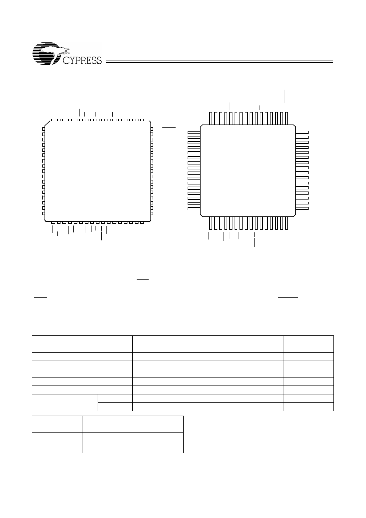
Pin Configurations
EF
10
11
12
13
14
15
16
17
18
19
20
21
22
23
24
67
Top View
60
59
58
57
56
55
54
53
52
51
50
49
48
3132 3334 353637383940 4142 43
5 4 3 2 1 68 66 65 64 63 62 61
Q
14
Q
13
GND
Q
12
Q
11
V
CC
Q
10
Q
9
GND
Q
8
Q
7
V
CC
D
14
D
13
D
12
D
11
D
10
D
9
V
CC
D
8
GND
D
7
D
6
D
5
D
4
2728 2930
987 6
47
46
45
44
Q
6
Q
5
GND
Q
4
D
3
D
2
D
1
D
0
25
26
VCC/SMODE
TQFP/STQFP
Top View
4255–2
1
2
3
4
5
6
7
8
9
10
11
12
13
14
15
48
47
46
45
44
43
42
41
40
39
38
37
36
35
34
33
17641863196220612160225923582457255626552754285329523051315032
49
16
PLCC
PAE
FL/RT
WCLK
WEN
WXI
VCCPAF
RXI
FF
WXO/HF
RXO
Q0Q
1
GND
Q2Q
3
V
CC
Q15GND
Q16Q17VCCEF
GND
VCCRS
OE
LD
REN
RCLK
GND
D17D16D
15
D
14
D
13
D
12
D
11
D
10
D
9
D
8
D
7
D
6
D
5
D
4
D
3
D
2
D
1
D
0
D
15
Q15GND
Q16Q
17
GND
V
CC
RS
OE
LD
REN
RCLK
GND
D17D
16
PAE
WCLK
WEN
WXI
V
CC
PAF
RXI
FF
WXO/HF
RXO
Q0Q
1
GND
Q2Q
3
Q
14
Q
13
GND
Q
12
Q
11
V
CC
Q
10
Q
9
GND
Q
8
Q
7
Q
6
Q
5
GND
Q
4
V
CC
V
CC
/SMODE
FL/RT
4255–3
CY7C4255
CY7C4265
CY7C4255
CY7C4265
Selection Guide
7C4255/65–10 7C4255/65–15 7C4255/65–25 7C4255/65–35
Maximum Frequency (MHz) 100 66.7 40 28.6
Maximum Access Time (ns) 8 10 15 20
Minimum Cycle Time (ns) 10 15 25 35
Minimum Data or Enable Set-Up (ns) 3 4 6 7
Minimum Data or Enable Hold (ns) 0.5 1 1 2
Maximum Flag Delay (ns) 8 10 15 20
Active Power Supply
Current (I
CC1
) (mA)
Commercial 45 45 45 45
Industrial 50 50 50 50
CY7C4255 CY7C4265
Density 8K x 18 16K x18
Package 64-pin
PLCC, TQFP,
STQFP
64-pin
PLCC, TQFP,
STQFP
CY7C4255
CY7C4265
3
Pin Definitions
Signal Name Description I/O Function
D
0 –17
Data Inputs I Data inputs for an 18-bit bus.
Q
0–17
Data Outputs O Data outputs for an 18-bit bus.
WEN Wr ite Enabl e I Enables the WCLK inpu.t
REN Read Enable I Enables the RCLK input.
WCLK Write Clock I The rising edge clocks data into the FIFO when WEN is LOW and the FIFO is not
Full. When LD
is asserted, WCLK writes data into the programmable flag-offset
register.
RCLK Read Clock I The rising edge cloc k s data out of the F IFO when REN is LOW and the FIFO is not
Empty. When LD
is asserted, RCLK r eads data out of the programmable flag- off-
set register.
WXO/HF Write Expansion
Out/Half Full Flag
O Dual-Mode Pin:
Single devi ce or width expansion – Half Full st atus flag.
Cascaded – Write Expansion Out signal, connected to WXI
of next device.
EF Empty Flag O When EF is LOW, the FIFO is empty. EF is synchronized to RCLK.
FF Full Flag O When FF is LOW, the FIFO is fu ll . F F i s synchronized to WCLK.
PAE Programmable
Almost Empty
O When PAE is LOW, the FIFO is almost empty based on the almost-empty offset
value pr ogram med into t he FIFO . PAE
is asynchr onous whe n VCC/SMODE is tied
to V
CC
; it is synchronized to RCLK when VCC/SMODE is tied to VSS.
PAF Programmable
Almost Full
O When PAF is LOW, the FIFO is almost full based on the almost full offset value
programmed into the FIFO. PAF
is asynchronous when VCC/SMODE is tied to
V
CC
; it is synchronized to WCLK when VCC/SMODE is tied to VSS.
LD Load I When LD is LOW, D
0–17
(Q
0–17
) are written (read) into (from) the programma-
ble-flag- offset register.
FL/RT First Load/
Retransmit
I Dual-Mode Pin:
Cascaded – The first device in the daisy chain will have FL
tied to VSS; all other
devices will have FL
tied to VCC. In st andard mode or width expansion, FL is tied
to V
SS
on all devi ce s.
Not Cascaded – Tied to V
SS
. Retransmit funct ion is also available in stand-alone
mode by strobing RT.
WXI Write Expansion
Input
I Cascaded – Connected to WXO of previous device.
Not Cascaded – Tied to V
SS
.
RXI Read Expansion
Input
I Cascaded – Connected to RXO of p r ev i o us device.
Not Cascaded – Tied to V
SS
.
RXO Read Expansion
Output
O Cascaded – Connected to RXI of next device.
RS Reset I Resets device to empty condition. A reset is required before an initial read or write
operation after power-up.
OE Output Enable I When OE is LOW, the FIFO’s data outputs drive the bus to which they are con-
nected. If OE
is HIGH, th e F IFO ’s outputs are in High Z (high-impedance) state.
VCC/SMODE Synchronous
Almost Empty/
Almost Full Flags
I Dual-Mode Pin:
Asynchronous Almost Empty/Almost Full flags – ti e d to V
CC
.
Synchronous Almost Empty/Almost Full flags – tied to V
SS
.
(Almost Empty synchronized to RCLK, Almost Full synchronized to WCLK.)
CY7C4255
CY7C4265
4
Maximum Ratings
(Above which the useful life may be impaired. For user guidelines, not tested.)
Storage Temperature ................................–65°C to +150 °C
Ambient Temperature with Power Applied .–55°C to +12 5 °C
Supply Voltage to Ground Potential...............–0.5V to +7.0V
DC V oltage Applied to Outputs
in High Z State............................................... –0.5V to +7.0V
DC Input Voltage..........................................−0.5V to V
CC
+0.5V
Output Current into Outputs (LOW).............................20 mA
Static Discharge Voltage .................... .......................>2001V
(per MIL–STD–883, Method 3015)
Latch-Up Current .....................................................>200 mA
Notes:
1. T
A
is the “Instant On” case temperature.
2. See the last page of this specification for Group A subgroup testing information.
3. The VIH and VIL specifications apply for all inputs except WXI, RXI. The WXI, RXI pin is not a TTL input. It is connected to either RXO, WXO of the
previous dev ice or V
SS
.
4. The VIH and VIL specifications apply for all inputs except WXI, RXI. The WXI, RXI pin is not a TTL input. It is connected to either RXO, WXO of the
previous dev ice or V
SS.
5. Input signals switch from 0V to 3V with a rise/fall time of less than 3 ns, clocks and clock enables switch at 20 MHz, while data inputs switch at 10 MHz. Outputs
are unloaded. ICC1(typ i c al) = (25mA+(freq –20 MHz)*(1.0 mA/MHz ))
6. All inputs = VCC – 0.2V, except RCLK and WCLK (which are switching at frequency = 20 MHz), and FL/RT which is at Vss. All outputs are unloaded.
7. Tested initially and after any design changes that may affect these parameters.
8. Tested initially and after any process changes that may affect these parameters.
Operating Range
Range
Ambient
Temperature
V
CC
Commercial 0°C to +70°C 5V ± 10%
Industrial
[1]
–40°C to +85°C 5V ± 10%
Electrical Characteristics
Over the Operating Range
[2]
7C42X5–10 7C42X5–15 7C42X5–25 7C42X5– 35
Parameter Description Test Conditions Min. Max. Min. Max. Min. Max. Min. Max. Unit
V
OH
Output HIGH Voltage VCC = Min. ,
I
OH
= –2.0 mA
2.4 2.4 2.4 2.4 V
V
OL
Output LOW Voltage VCC = Min. ,
I
OL
= 8.0 mA
0.4 0.4 0.4 0.4 V
V
IH
[3]
Input HIGH Voltage 2.0 V
CC
2.0 V
CC
2.0 V
CC
2.0 V
CC
V
V
IL
[4]
Input LOW Voltage –0.5 0.8 –0.5 0.8 –0.5 0.8 –0.5 0.8 V
I
IX
Input Leakage
Current
V
CC
= Max. –10 +10 –10 +10 –10 +10 –10 +10
µA
I
OZL
I
OZH
Output OFF,
High Z Current
OE > VIH,
V
SS
< VO < V
CC
–10 +10 –10 +10 –10 +10 –10 +10
µA
I
CC1
[5]
Active Power Supply
Current
Com’l 45 45 45 45 mA
Ind 50 50 50 50 mA
I
CC2
[6]
Average Standby
Current
Com’l 10 10 10 10 mA
Ind 15 15 15 15 mA
Capacitance
[7, 8]
Parameter Description Test Conditions Max. Unit
C
IN
Input Capacitance TA = 25°C, f = 1 M Hz,
V
CC
= 5.0V
5 pF
C
OUT
Output Capacitance 7 pF
CY7C4255
CY7C4265
5
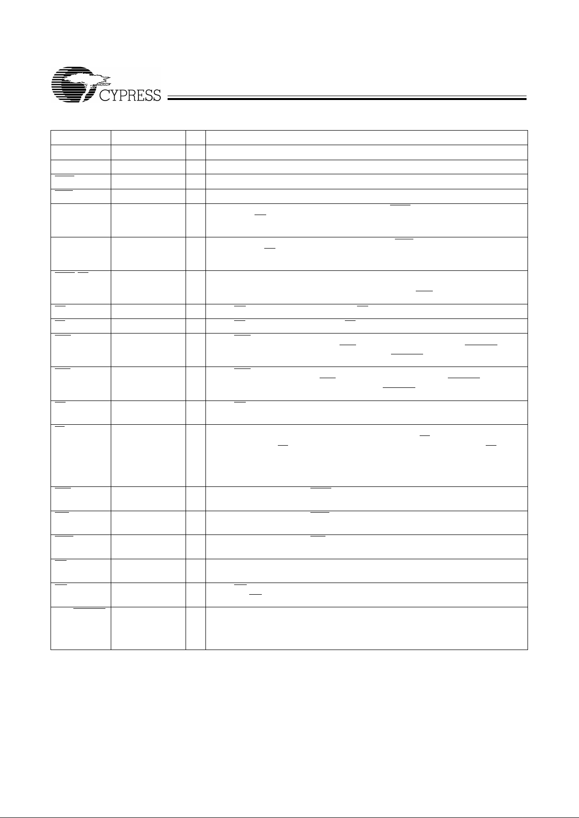
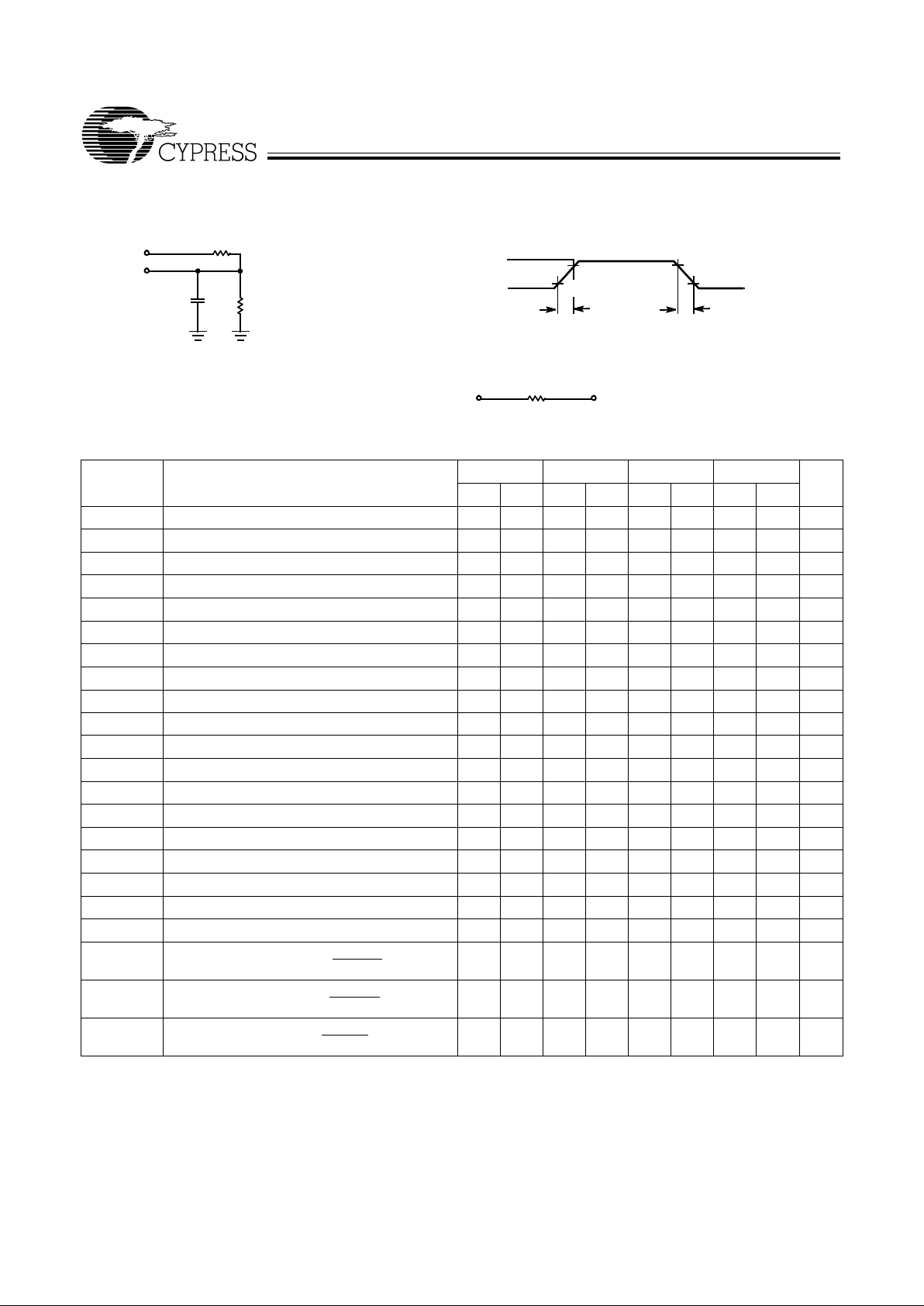
AC Test Loads and Waveforms
[9, 10]
3.0V
5V
OUTPUT
R1 1.1 K
Ω
R2
680
Ω
C
L
INCLUDING
JIG AND
SCOPE
GND
90%
10%
90%
10%
≤
3ns
≤
3
ns
OUTPUT 1.91V
Equivalentto: THÉ VENIN EQUIVALENT
4255–4
410
Ω
ALL INPUT PULSES
4255–5
Switching Characteristics
Over the Operating Range
7C42X5–10 7C42X5–15 7C42X5–25 7C42X5–35
Parameter Description Min. Max. Min. Max. Min. Max. Min. Max. Unit
t
S
Clock Cycle Frequency 100 66.7 40 28.6 MHz
t
A
Data Access Time 2 8 2 10 2 15 2 20 ns
t
CLK
Clock Cycle Time 10 15 25 35 ns
t
CLKH
Clock HIGH Time 4.5 6 10 14 ns
t
CLKL
Clock LOW Time 4.5 6 10 14 ns
t
DS
Data Set-Up Time 3 4 6 7 ns
t
DH
Data Hold Time 0.5 1 1 2 ns
t
ENS
Enable Set-Up Time 3 4 6 7 ns
t
ENH
Enable Hold Time 0.5 1 1 2 ns
t
RS
Reset Pulse Width
[11]
10 15 25 35 ns
t
RSR
Reset Recovery Time 8 10 15 20 ns
t
RSF
Reset to Flag and Output Time 10 15 25 35 ns
t
PRT
Retransmit Pulse Width 30 35 45 55 ns
t
RTR
Retransmit Recov ery Time 60 65 75 85 ns
t
OLZ
Output Enable to Output in Low Z
[12]
0 0 0 0 ns
t
OE
Output Enable to Output Valid 3 7 3 8 3 12 3 15 ns
t
OHZ
Output Enable to Output in High Z
[12]
3 7 3 8 3 12 3 15 ns
t
WFF
Write Clock to Full Flag 8 10 15 20 ns
t
REF
Read Clock to Empty Flag 8 10 15 20 ns
t
PAFasynch
Clock to Programm able Almost-Full Flag
[13]
(Asynchronous mode, VCC/SMODE tied to VCC)
12 16 20 25 ns
t
PAFsynch
Clock to Programm able Almost-Full Flag
(Synchronous mode, V
CC
/SMODE tied to VSS)
8 10 15 20 ns
t
PAEasynch
Clock to Programm able Almost-Empty Flag
[13]
(Asynchronous mode, VCC/SMODE tied to VCC)
12 16 20 25 ns
Notes:
9. C
L
= 30 pF for all AC parameters except for t
OHZ
.
10. CL = 5 pF for t
OHZ
.
11. Pulse widths less than minimum values are not allowed.
12. Values guaranteed by design, not currently tested.
13. t
PAFasynch
, t
PAE asynch
, after program register write will not be valid until 5 ns + t
PAF(E)
.
CY7C4255
CY7C4265
6
t
P AEsynch
Clock to Programm able Almost-Full Flag
(Synchronous mode, V
CC
/SMODE tied to VSS)
8 10 15 20 ns
t
HF
Clock to Half-Full Flag 12 16 20 25 ns
t
XO
Clock to Expansi on Out 6 10 15 20 ns
t
XI
Expansion in Pulse Width 4.5 6.5 10 14 ns
t
XIS
Expansion in Set-Up Time 4 5 10 15 ns
t
SKEW1
Skew Time between Read Clock and Write
Clock for Full Flag
5 6 10 12 ns
t
SKEW2
Skew Time between Read Clock and Write
Clock for Empty Flag
5 6 10 12 ns
t
SKEW3
Skew Time between Read Clock and Write
Clock f or Progr ammable Almost Empty and Programmabl e Almost Full Flags (Synch ronous
Mode only)
10 15 18 20 ns
Switching Characteristics
Over the Operating Range (continued)
7C42X5–10 7C42X5–15 7C42X5–25 7C42X5–35
Parameter Description Min. Max. Min. Max. Min. Max. Min. Max. Unit
CY7C4255
CY7C4265
7
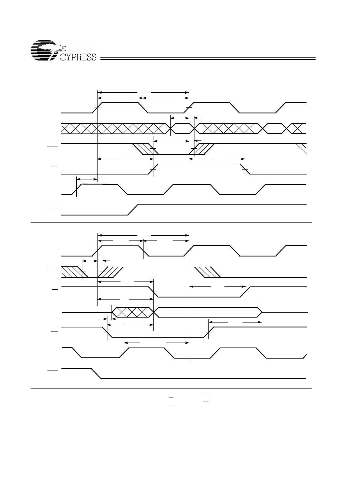
Switching Waveforms
Notes:
14. t
SKEW1
is the minimum t ime betw een a risin g RCLK edge a nd a r ising WC LK edge t o guar an tee that F F w ill g o HIGH during the c urrent cloc k c ycle. If the time betw een
the rising edge of R CLK and the ri sing edge of W CLK is l ess than t
SKEW1
, then FF ma y not ch ange stat e until th e ne x t WCLK rising edge .
15. t
SKEW2
is the minimum t ime betw een a risin g WCLK ed ge and a rising RC LK edge t o guar an tee that E F will go HIGH during the current clock cycle. It the time between
the rising edge of WC LK and t he ris ing edge of R CLK is l ess than t
SKEW2
, then EF ma y no t change state un ti l the ne xt RCLK r ising edge.
Write Cycle Timing
t
CLKH
t
CLKL
NO OPERATION
t
DS
t
SKEW1
t
ENS
WEN
t
CLK
t
DH
t
WFF
t
WFF
t
ENH
WCLK
D
0–D17
FF
REN
RCLK
4255–6
[14]
Read CycleTiming
t
CLKH
t
CLKL
NO OPERATION
t
SKEW2
WEN
t
CLK
t
OHZ
t
REF
t
REF
RCLK
Q
0–Q17
EF
REN
WCLK
OE
t
OE
t
ENS
t
OLZ
t
A
t
ENH
VALID DATA
4255–7
[15]

CY7C4255
CY7C4265
8
Notes:
16. The clocks (RCLK, WCLK) can be free-running during reset.
17. After reset, the outputs will be LOW if OE
= 0 and three- state if O E = 1.
18. When t
SKEW2
> minimum specification, t
FRL
(maximum) = t
CLK
+ t
SKEW2
. When t
SKEW2
< minimum specific ation, t
FRL
(maximum) = ei ther 2*t
CLK
+ t
SKEW2
or t
CLK
+
t
SKEW2
. The Latency T iming appli es only at the Empt y Boundary (EF = LOW ).
19. The first word is available the cycle after EF goes HIGH, a lwa ys .
Switching Waveforms
(continued )
Reset Timing
t
RS
t
RSR
Q
0 –Q17
RS
t
RSF
t
RSF
t
RSF
OE=1
OE
=0
REN
,WEN,
LD
EF,PAE
FF,PAF,
HF
4255–8
[16]
[17]
D
0
(FIRSTVALIDWRITE)
First Data Word Latency after Reset with Simultaneous Read and Write
t
SKEW2
WEN
WCLK
Q
0–Q17
EF
REN
OE
t
OE
t
ENS
t
OLZ
t
DS
RCLK
t
REF
t
A
t
FRL
D
1
D
2
D
3
D
4
D
0
D
1
D0–D
17
4255–9
t
A
[18]
[19]

CY7C4255
CY7C4265
9
Switching Waveforms
(continued )
D1D0
t
ENS
t
SKEW2
Empty Flag Timing
WEN
WCLK
Q
0–Q17
EF
REN
OE
t
DS
t
ENH
RCLK
t
REF
t
A
t
FRL
D0–D
17
D0
t
SKEW2
t
FRL
t
REF
t
DS
t
ENS
t
ENH
4255–10
t
REF
[18]
[18]
NEXT DATA READ
DATA WRITE
NO WRITE
DATA IN OUTPUT REGISTER
FullFlagTiming
FF
WCLK
Q
0–Q17
REN
OE
RCLK
t
A
D0–D
17
DATA READ
t
SKEW1
t
DS
t
ENS
t
ENH
WEN
t
WFF
t
A
t
SKEW1
t
ENS
t
ENH
t
WFF
DATA WRITE
NO WRITE
t
WFF
LOW
4255–11
[14]
[14]

CY7C4255
CY7C4265
10
Note:
20. PAE
is offset = n. Number of data w ords into F IFO already = n.
Switching Waveforms
(continued )
t
ENH
Half-Full Flag Timing
WEN
WCLK
HF
REN
RCLK
t
CLKH
t
HF
t
ENS
HALF FULL + 1
OR MORE
t
CLKL
t
ENS
HALF FULLORLESS HALF FULLOR LESS
t
HF
4255–12
t
ENH
Programmable Almost Empty Flag Timing
WEN
WCLK
PAE
[20]
REN
RCLK
t
CLKH
t
PAE
t
ENS
N + 1 WORDS
IN FIFO
t
CLKL
t
ENS
t
PAE
n WORDS IN FIFO
4255–13

CY7C4255
CY7C4265
11
Notes:
21. PAE offset − n.
22. t
SKEW3
is the minim um t ime betw een a rising W CLK an d a rising RC LK edge f or PAE to change stat e dur ing th at cl ock cyc le. If the time be twee n th e edge of WCLK an d
the rising RCLK is less t han t
SKEW3
, then PAE ma y not change state unti l th e ne xt RC LK.
23. If a read is preformed on this rising edge of the read clock, there will be Empty + (n−1) words in the FIFO when PAE goes LO W.
24. PAF offset = m. Number of data words written into FIFO already = 8192 − (m + 1) for the CY7C4255 and 16384 − (m + 1) for the CY7C4265.
25. PAF is offset = m.
26. 8192
−
m words in CY7C4255 and 16384 – m words in CY7C4265.
27. 8192 − (m + 1) words in CY7C4255 and 16384 – (m + 1) CY7C4265.
Switching Waveforms
(continued )
Note
t
ENH
Programmable Almost Empty Flag Timing (applies only in SMODE (SMODE is LOW))
WCLK
PAE
RCLK
t
CLKH
t
ENS
t
CLKL
t
ENS
t
PAE synch
N + 1 WORDS
INFIFO
4255–14
t
ENH
t
ENS
t
ENH
t
ENS
t
PAE synch
REN
WEN
WEN2
t
SKEW3
Note
[22]
21
23
Note
t
ENH
Programmable Almost Full Flag Timing
WEN
WCLK
PAF
REN
RCLK
t
CLKH
t
PAF
t
ENS
t
CLKL
t
ENS
t
PAF
4255–15
FULL– M WORDS
INFIFO
FULL– (M+1) WORDS
IN FIFO
[27]
[26]
24
[25]

CY7C4255
CY7C4265
12
Notes:
28. If a write is performed on this rising edge of the write clock, there will be Full − (m−1) words of the FIFO when PAF
goes LOW.
29. PAF offset = m.
30. t
SKEW3
is the minimum t ime betw een a risin g RCLK and a rising WCLK edge f or PAF to change state during that clock cycle. If the time between the edge of RCLK and
the rising edge of WC LK i s less th an t
SKEW3
, then P AF may no t change st ate unt il the ne x t WCLK rising edge .
Switching Waveforms
(continued )
Note
Note
t
ENH
Programmable Almost Full Flag Timing (applies only in SM ODE (SMODE is LOW))
WCLK
PAF
RCLK
t
CLKH
t
ENS
FULL– M WORDS
IN FIFO
t
CLKL
t
ENS
FULL– M + 1 WORDS
IN FIFO
4255–16
t
ENH
t
ENS
t
ENH
t
ENS
t
PAF
REN
WEN
WEN2
t
SKEW3
t
PAF synch
28
29
[26]
[30]
t
ENH
Write Programmable Registers
LD
WCLK
t
CLKH
t
ENS
t
CLKL
PAE OFFSET
D
0–D17
WEN
t
ENS
PAF OFFSET
PAE OFFSET
t
CLK
D0–
D
11
t
DS
t
DH
4255–17

CY7C4255
CY7C4265
13
Notes:
31. Write to Last Physical Location.
32. Read from Last Physical Location.
Switching Waveforms
(continued )
t
ENH
Read Programmable Registers
LD
RCLK
t
CLKH
t
ENS
t
CLKL
PAE OFFSET
Q
0–Q17
WEN
t
ENS
PAF OFFSET PAE OFFSET
t
CLK
UNKNOWN
t
A
4255–18
Write ExpansionOut Timing
WEN
WCLK
WXO
t
CLKH
t
ENS
t
XO
t
XO
4255–19
Note 31
Note 31
Read Expansion OutTiming
REN
WCLK
RXO
t
CLKH
t
ENS
t
XO
t
XO
4255–20
Note 32
Write Expansion In Timing
WCLK
WXI
t
XI
t
XIS
4255–21

CY7C4255
CY7C4265
14
Notes:
33. Clocks are free-running in this case.
34. The flags may change state during Retransmit as a result of the offset of the read and write pointers, but flags will be valid at t
RTR
.
35. For the synchronous PAE and PAF flags (SMODE), an appropriate c lock cycle is neces sary after t
RTR
to update the se flags .
Switching Waveforms
(continued )
Read Expansion In Timing
RCLK
RXI
t
XI
t
XIS
4255–22
Retransmit Timing
REN/WEN
FL/RT
t
PRT
t
RTR
4255–23
EF/FF
and all
async flags
HF/PAE/PAF
[33, 34, 35]

CY7C4255
CY7C4265
15
Architecture
The CY7C4256/65 consist s of an arra y of 8K/16K words of 18
bits each (implemente d by a dual-po rt arra y of SRAM cells), a
read pointer, a write pointer, control signals (RCLK, WCLK,
REN
, WEN, RS), and flags (EF, PAE, HF, PAF, FF). The
CY7C4255/65 also includes the control signals WXI
, RXI, WXO,
RXO
for depth expansion.
Resetting the FIFO
Upon power-up, the FIFO must be reset with a Reset (RS)
cycle. This causes the FIFO to enter the Empty condition signified by
EF
being LOW. All data outputs go LOW after the falling edge of RS
only if OE is asserted. In order for the FIFO to reset to its default state,
a falling edge must occur on RS
and the user must not read or write
while RS
is LOW.
FIFO Operation
When the WEN signal is active (LOW), data present on the D
0–17
pins is written into the FIFO on each rising edge of the WCLK signal.
Similarly, when the REN
signal is active LO W , data in the FIFO mem-
ory will be presented on the Q
0–17
outputs. New data will be present-
ed on each rising edge of RCLK while REN
is active LOW and OE is
LOW. REN
must set up t
ENS
before RCLK for it to be a valid read
function. WEN
must occur tENS before WCLK for it to be a valid write
function.
An output enable (OE
) pin is provided to three-state the Q
0 – 17
outputs when OE is deasserted. When OE is enabled (LOW), data
in the output register will be available to the Q
0–17
outputs after tOE.
If devices are cascaded, the OE
function will only output data on the
FIFO that is read enabled.
The FIFO contains overflow circuitry to disallow additional
writes when the F IFO is full, and under fl ow circ uitry to disa llow
additional reads when the FIFO is empty. An empty FIFO
maintains the data of the last valid read on its Q
0–17
outputs
even after additional reads occur .
Programming
The CY7C4255/65 devices contain two 14-bit offset registers.
Data present on D
0–13
during a program write will determin e the
distance from Empty (Full) that the Almost Empty (Almost Full) flags
become active. If the user el ects not to program the FIFO’s flags, the
default offset values are used (see Table 2 ). When the Load LD
pin
is set LOW and WEN
is set LOW, data on the inputs D
0–13
is written
into the Empty offset register on the first LOW-to-HIGH transition of
the Write Clock (WCLK). When the LD
pin and WEN are held LOW
then data is written into the Full offset register on the second
LOW-to-HIGH transition of the Write Clock (WCLK). The third transition of the Write Clock (WCLK) again writes to the Empty offset register (see Table 1). Writing all offset registers does not have to occur
at one time. One or two offset registers can be written and then, by
bringing the LD
pin HIGH, the FIFO is returned to normal read/write
operation. When the LD
pin is set LOW, and WEN is LOW, the next
offset register in sequence is written.
The contents of the offset registers can be read on the output
lines when the LD
pin is set LOW and REN is set LOW; then, data
can be read on the LOW-to-HIGH transition of the Read Clock
(RCLK).
Flag Ope r ati o n
The CY7C4255/65 devi ces provide fiv e flag pins to indic ate the
condition of the FIFO contents. Empty and Full are synchronous. PAE
and P A F are synchronous if VCC/SMODE is tied to VSS.
Full Flag
The Full Flag (FF
) will go LOW when device is Full. Write operations
are inhibited whenever FF
is LOW regardless of the state of WEN. FF
is synchronized to WCLK, i.e., it is exclusively updated by each rising
edge of WCLK.
Empty Flag
The Empty Flag (EF
) will go LOW when the device is empty. Read
operations are inhibited whenever EF
is LOW , regardless of the state
of REN
. EF is synchronized to RCLK, i.e., it is exclusively updated by
each rising edge of RCLK.
Programmable Almost Empty/Almost Full Flag
The CY7C4255/65 feat ures pr ogram mab le Almos t Empty and
Almost Full Flags. Each flag can be programmed (described
in the Programming section) a specific distance f rom the corresponding boundary flags (Empty or Full). When the FIFO
contains the number of words or fe wer f or which the fla gs have
been programm ed, th e PAF
or P AE wil l be asserted, signifying that
the FIFO is either Almost Full or Almost Empty. See Ta b l e 2 for a
description of programmable flags.
When the SMODE
pin is tied LOW, the PAF flag signal transition is
caused by the rising edge of the write clock and the P AE
flag transition
is caused by the rising edge of the read clock.
Notes:
36. The same selection sequence applies to reading from the registers. REN
is enabled and read i s perf ormed on the LO W-to-HIGH transition of RCLK.
Table 1. Write Offset Register
LD WEN WCLK
[36]
Selection
0 0 Writing to offset registers:
Empty Offset
Full Offset
0 1 No Operation
1 0 Write Into FIFO
1 1 No Operation

CY7C4255
CY7C4265
16
Retransmit
The retransmit feature is beneficial when transferring packets
of data. It enables the receipt of data to be acknowledged by
the receiv er and retransmitted if necessary.
The Retransmit (RT) input is active in the stand-alone and
width expa nsion modes . The retr ansmit f eat ur e is intended f or
use when a number of writes equal to or less than the depth
of the FIFO have occurred and at least one word has been
read since the last RS
cycle. A HIGH pulse on RT resets t he inter-
nal read pointer to the first physical location of the FIFO. WCLK and
RCLK may be free running but must be disabled during and t
RTR
after
the retransmit pulse. With every valid read cycle after retransmit, previously accessed data is read and the read point er is incremented
until it is equal to the write pointer. Flags are gov erned by the relative
locations of the read and w rite pointers and ar e updated during a
retransmit cycle. Data written to the FIFO a fter activation of RT are
tran sm itt ed a ls o.
The full depth of the FIFO can be rep eatedly retransmitted.
Table 2. Flag Truth Table
Number of Words in FIFO
FF PAF HF PAE EFCY7C4255 – 8K x 18 CY7C4265 – 16K x 18
0 0 H H H L L
1 to n
[37]
1 to n
[37]
H H H L H
(n+1) to 4096 (n+1) to 819 2 H H H H H
4097 to (8192–(m+1)) 8193 to (16384 –(m+1)) H H L H H
(8192–m)
[38]
to 8191 (16384–m)
[38]
to 16383 H L L H H
8192 16384 L L L H H
Notes:
37. n = Empty Offset (Default Values: CY7C4255/CY7C4265 n = 127).
38. m = Full Offset (Default Values: CY7C4255/CY7C4265 n = 127).

CY7C4255
CY7C4265
17
Width Expansion Configuration
The CY7C4255/65 can be expanded in width to pr ovide word
widths greater than 18 in increments of 18. During width expansion mode all control line inputs are common and all flags
are availabl e. Empty (Ful l) flags should be created by ANDing
the Empty (Full) flags of every FIFO; the PAE
and PAF flags
can be detected f rom any o ne devic e. This t echnique wi ll avoi d
reading data from, or writing data to the FIFO that is “stag-
gered” by one clock cycle due to the variations in skew between RCLK and WCLK. Figure 1 demonstrates a 36-word width
by using two CY7C4255/65s.
Figure 1. Block Diagram of 8K x18/ 16K x 18 Synchronous FIFO Memory Used in a Width Expansion Configuration
4255–24
FF
FF EF
EF
WRITE CLOCK(WCLK)
WRITE ENABLE (WEN
)
LOAD(LD
)
PROGRAMMABLE(PAE
)
HALF FULL FLAG (HF
)
FULL FLAG (FF
)
7C4255
7C4265
1836
DATA IN (D)
RESET
(RS)
18
RESET(RS)
READ CLOCK (RCLK)
READ ENABLE (REN
)
OUTPUT ENABLE (OE
)
PROGRAMMABLE (PAF
)
EMPTY FLAG
(EF)
18
DATA OUT(Q)
18 36
FIRST LOAD (FL)
WRITE EXPANSION IN (WXI
)
READ EXPANSION IN (RXI
)
7C4255
7C4265

CY7C4255
CY7C4265
18
Depth Expansion Configuration
(with Programmable Flags)
The CY7C4255/65 can easily be adapted to applications requiring more than 8192/16384 words of buffering. Figure 2
shows Depth Expansion using three CY7C42X5s. Maximum depth
is limited only by signal loading. Follow these steps:
1. The first device must be de signated by grounding the Firs t
Load (FL
) control input.
2. All other devices must have FL
in the HIGH state.
3. The Write Expansion Out (WXO
) pin of each device must be
tied to the Write Expansion In (WXI
) pin of the next devi ce.
4. The Read Expansion Out (RXO
) pin of each device must be
tied to the Read Expansion In (RXI
) pin of the next devi ce.
5. All Load (LD
) pins are tied together.
6. The Half-Full Fl ag (H F
) is not available in the Depth Expansion
Configuration.
7. EF
, FF, PAE, and PAF are creat ed with composite flags by
ORing together these respective flags for monitoring. The
composite PAE
and PAF flags ar e not prec ise.
Figure 2. Block Diagram of 8Kx18/ 16Kx18 Synchro nous FIFO Memory
with Programmabl e Flags used in Depth Expansion Configuration
4255–25
WRITE CLOCK(WCLK)
WRITE ENABLE
(WEN)
RESET
(RS)
LOAD
(LD)
FF
PAF
PAF
FF EF
PAE
PAE
EF
WXI RXI
FIRST LOAD(FL)
READ CLOCK
(RCLK)
READ ENABLE
(REN)
OUTPUT ENABLE
(OE)
WXO
RXO
PAF
FF EF
PAE
WXI RXI
WXO RXO
V
CC
FL
PAF
FF EF
PAE
WXI RXI
WXO RXO
7C4255
7C4265
V
CC
FL
DATA IN(D) DATA OUT(Q)
7C4255
7C4265
7C4255
7C4265
CY7C4255
CY7C4265
19
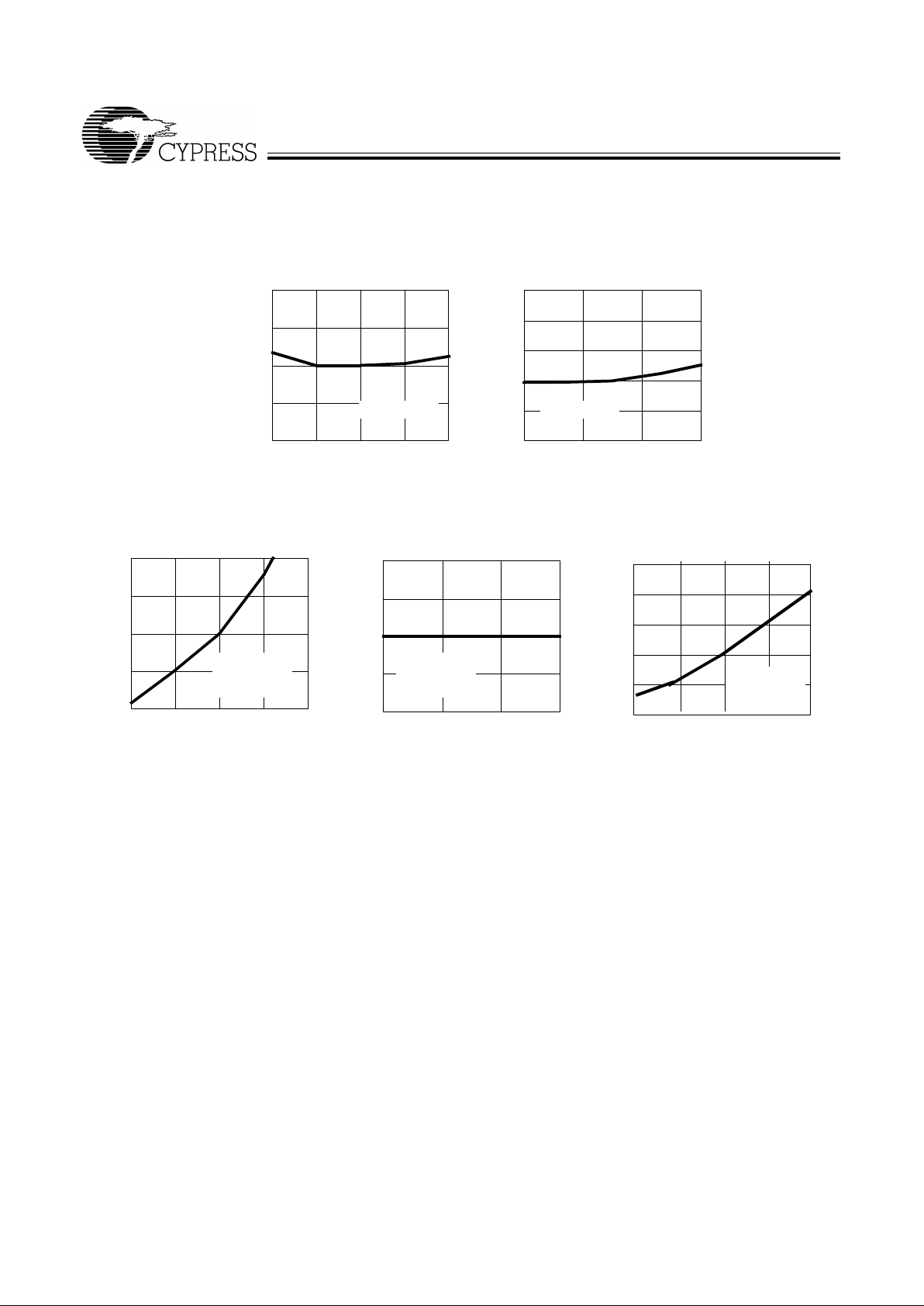
T y pical AC and DC Characteristics
0.60
0.80
1.00
1.20
1.40
1.60
−
55.00 5.00 65.00
125.00
0.80
0.90
1.00
1.10
1.20
4.00 4.50 5.00 5.50
6.00
SUPPLY VOLTAGE(V)
NORMALIZED t
A
vs. SUPPLY
VOLTAGE
NORMALIZED SUPPLY CURRENT
vs. SUPPLY VOLTAGE
NORMALIZED t
A
vs. AMBIENT
TEMPERATURE
AMBIENT TEMPERATURE(
°
C)
NORMALIZED SUPPLY CURRENT
vs. AMBIENT
TEMPERATURE
T
A
= 25°C
FREQUENCY (MHz)
NORMALIZED SUPPLY
CURRENT
vs. FREQUENCY
SUPPLY VOLTAGE (V)
VCC= 5.0V
NORMALIZED I
CC
NORMALIZED t
A
NORMALIZED t
A
0.60
0.80
1.00
1.20
1.40
4.00 4.50 5.00 5.50
6.00
NORMALIZED I
CC
AMBIENT TEMPERATURE (°C)
V
IN
= 3.0V
T
A
= 25°C
f= 28
MHz
0.80
0.90
1.00
1.10
1.20
−
55.00 5.00 65.00
125.00
V
IN
= 3.0V
V
CC
= 5.0V
f= 28MHz
NORMALIZED I
CC
0.50
0.75
1.00
1.25
1.50
1.75
20.00 30.00 40.00 50.00
60.00
V
CC
= 5.0V
T
A
= 25°C
V
IN
= 3.0V

CY7C4255
CY7C4265
20
Document #: 38- 00468-C
Ordering Information
8Kx18 Deep Sync FIFO
Speed
(ns)
Ordering Code
Package
Name
Package
Type
Operating
Range
10 CY7C4255–10AC A65 64-Lead Thin Quad Flatpack Commercial
CY7C4255–10JC J81 68-Lead Plastic Leaded Chip Carrier
CY7C4255-10ASC A64 64-Lead Small Thin Quad Flatpack
CY7C4255–10AI A65 64-Lead Thin Quad Flatpack Industrial
CY7C4255–10JI J81 68-Lead Plastic Leaded Chip Carrier
15 CY7C4255–15AC A65 64-Lead Thin Quad Flatpack Commercial
CY7C4255–15JC J81 68-Lead Plastic Leaded Chip Carrier
CY7C4255-15ASC A64 64-Lead Small Thin Quad Flatpack
CY7C4255–15AI A65 64-Lead Thin Quad Flatpack Industrial
CY7C4255–15JI J81 68-Lead Plastic Leaded Chip Carrier
25 CY7C4255–25AC A65 64-Lead Thin Quad Flatpack Commercial
CY7C4255–25JC J81 68-Lead Plastic Leaded Chip Carrier
CY7C4255-25ASC A64 64-Lead Small Thin Quad Flatpack
CY7C4255–25AI A65 64-Lead Thin Quad Flatpack Industrial
CY7C4255–25JI J81 68-Lead Plastic Leaded Chip Carrier
35 CY7C4255–35AC A65 64-Lead Thin Quad Flatpack Commercial
CY7C4255–35JC J81 68-Lead Plastic Leaded Chip Carrier
CY7C4255–35AI A65 64-Lead Thin Quad Flatpack Industrial
CY7C4255–35JI J81 68-Lead Plastic Leaded Chip Carrier
16Kx18 Deep Sync FIFO
Speed
(ns)
Ordering Code
Package
Name
Package
Type
Operating
Range
10 CY7C4265–10AC A65 64-Lead Thin Quad Flatpack Commercial
CY7C4265–10JC J81 68-Lead Plastic Leaded Chip Carrier
CY7C4365-10ASC A64 64-Lead Small Thi n Quad Flatpack
CY7C4265–10AI A65 64-Lea d Thin Quad Fl atpack Industrial
CY7C4265–10JI J81 68-Lead Plastic Leaded Chip Carrier
15 CY7C4265–15AC A65 64-Lead Thin Quad Flatpack Commercial
CY7C4265–15JC J81 68-Lead Plastic Leaded Chip Carrier
CY7C4265-15ASC A64 64-Lead Small Thi n Quad Flatpack
CY7C4265–15AI A65 64-Lea d Thin Quad Fl atpack Industrial
CY7C4265–15JI J81 68-Lead Plastic Leaded Chip Carrier
25 CY7C4265–25AC A65 64-Lead Thin Quad Flatpack Commercial
CY7C4265-25ASC A64 64-Lead Small Thi n Quad Flatpack
CY7C4265–25JC J81 68-Lead Plastic Leaded Chip Carrier
CY7C4265–25AI A65 64-Lea d Thin Quad Fl atpack Industrial
CY7C4265–25JI J81 68-Lead Plastic Leaded Chip Carrier
35 CY7C4265–35AC A65 64-Lead Thin Quad Flatpack Commercial
CY7C4265–35JC J81 68-Lead Plastic Leaded Chip Carrier
CY7C4265–35AI A65 64-Lea d Thin Quad Fl atpack Industrial
CY7C4265–35JI J81 68-Lead Plastic Leaded Chip Carrier

CY7C4255
CY7C4265
21
Package Diagrams
64-Pin Thin Plastic Quad Flat Pack (10 x 10 x 1.4 mm) A64
51-85051-A

CY7C4255
CY7C4265
© Cypress Semiconductor Corporation, 2000. The information contained herein is subject to change without notice. Cypress Semiconductor Corporation assumes no responsibility for the use
of any circuitry other than circuitry embodied in a Cypress Semiconductor product. Nor does it con vey or imply any license under patent or other rights. Cypress Semiconductor does not authorize
its products for use as critical components in life-support systems where a malfunction or failure may reasonably be expected to result in significant injury to the user. The inclusion of Cypress
Semiconductor products in life-support systems application implies that the manufacturer assumes all risk of such use and in doing so indemnifies Cypress Semiconductor against all charges.
Package Diagrams
(continued)
64-Lead Thin Plastic Quad Flat Pack (14 x 14 x 1.4 mm) A65
51-85046-B
68-Lead Plastic Leaded Chip Carrier J81
51-85005-A
 Loading...