

Cypress Semiconductor CY7C4421-15JC, CY7C4421-15AC, CY7C4421-10JC, CY7C4421-10AC, CY7C4421-25JCT Datasheet
...
32K x 16 Static RAM
CY7C1020
Cypress Semiconductor Corporation
• 3901 North First Street • San Jose • CA 95134 • 408-943-2600
October 18, 1999
7C10
Features
• 5.0V operation (± 10%)
• High speed
—t
AA
= 10 ns
• Low active power
—825 mW (max., 10 ns, “L” version)
• Very L ow standb y p ow e r
—550 µW (max., “L” version)
• Automat ic power-down when deselected
• Independent Control of Upper and Lower bytes
• Available in 44-pin TSOP II and 400-mil SOJ
Functional Description
The CY7C1020 is a high-performance CMOS static RAM organized as 32,768 words by 16 bits. This device has an automatic power-down feature that significantly reduces power
consumption when deselected.
Writing to the device is accomplished by taking Chip Enable
(CE
) and Write Enable (WE) inputs LOW. If Byte Low Enable
(BLE
) is LOW, then data from I/O pins (I/O1 through I/O8), is
written into the location specified on the address pins (A
0
through A14). If Byte High Enable (BHE) is LOW, then data
from I/O pins (I/O
9
through I/O16) is written into the location
specified on the address pins (A
0
through A14).
Reading from the device is accomplished by taking Chip Enable (CE
) and Output Enable (O E) LOW whil e for cing the Write
Enable (WE
) HIGH. If Byte Low Enable (BLE) is LOW, then
data from the memory location specified by the address pins
will appear on I /O
1
to I/O8. If Byte High Enable (BHE) is LOW ,
then data from memory will appear on I/O
9
to I/O16. See the
truth table a t the bac k of this dat a sheet f or a c omplete des cription of read and write modes.
The input/output pins (I/O
1
through I/O16) are placed in a
high-impedance state when the device is deselected (CE
HIGH), the outputs are disab led (OE HIGH ), the BHE and BLE
are disabl ed (BHE, BLE HIGH), or during a write oper ation (CE
LOW, and WE LOW).
The CY7C1020 is available in standard 44-pin TSOP type II
and 400-mil-wide SOJ packages.
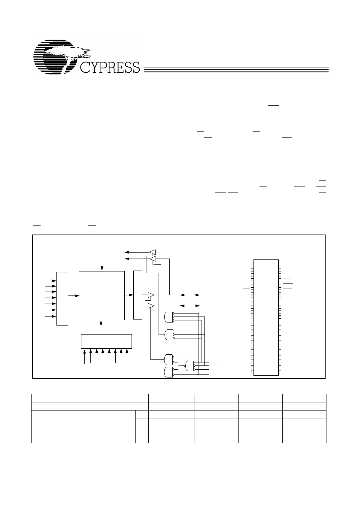
WE
Logic Block Diagram
Pin Configuration
1
2
3
4
5
6
7
8
9
10
11
14
31
32
36
35
34
33
37
40
39
38
Top View
SOJ / TSOP II
12
13
41
44
43
42
16
15
29
30
V
CC
A
10
A
9
A
8
A
7
NC
NC
A
14
OE
V
SS
A
0
I/O
16
A
13
CE
I/O
3
I/O
1
I/O
2
BHE
NC
A
12
A
11
1020-2
18
17
20
19
I/O
4
27
28
25
26
22
21
23
24
NC
V
SS
I/O
7
I/O
5
I/O
6
I/O
8
A
1
A
2
BLE
V
CC
I/O
15
I/O
14
I/O
13
I/O
12
I/O
11
I/O
10
I/O
9
A
3
A
4
A
5
A
6
32K x 16
RAM Array
I/O
1
– I/O
8
ROW DECODER
A
6
A
5
A
4
A
3
A
0
COLUMN DECODER
A
9
A10A11A12A13A
14
SENSE AMPS
DATA IN DRIVERS
OE
A
2
A
1
I/O9 – I/O
16
CE
WE
BLE
BHE
A
8
A
7
1020-1
Selection Guide
7C1020-10 7C1020-12 7C1020-15 7C1020-20
Maximum Access Time (ns) 10 12 15 20
Maximum Operating Curr ent (mA) 180 170 160 160
L150 140 130 130
Maximum CMOS Standby Current (mA) 3 3 3 3
L 0.1 0.1 0.1 0.1
CY7C1020
2
Maximum Ratings
(Above which the useful lif e m ay be impaired. For user guidelines, not tested.)
Storage Temperature .................................–65°C to +15 0°C
Ambient Temperature with
Power Applied.............................................–55°C to +125°C
Supply Voltage on V
CC
to Relative GND
[1]
....–0.5V to +7.0V
DC V oltage Applied to Outputs
in High Z State
[1]
.....................................–0.5V to VCC +0.5V
DC Input Voltage
[1]
..................................–0.5V to VCC +0.5V
Curre n t in to Out p ut s (L OW )........ .. .. .......... ... ......... ... .... 20 mA
Static Discharge Voltage .......... ......................... .. ......>2001V
(per MIL-STD-883, Method 3015)
Latch-Up Current.....................................................>200 mA
Operating Range
Range
Ambient
Temperature
[2]
V
CC
Commercial 0°C to +70°C 4.5V–5.5V
Electrical Characteristics
Over the Operating Range
Parameter Description Tes t Condi ti ons
7C1020-10
7C1020-12 7C1020-15
UnitMin. Max. Min. Ma x. Min. Max.
V
OH
Output HIGH Voltage VCC = Min., IOH = –4.0 mA 2. 4 2.4 2.4 V
V
OL
Output LOW Voltage VCC = Min., IOL = 8.0 mA 0.4 0.4 0.4 V
V
IH
Input HIGH Voltage 2.2 6.0 2.2 6.0 2.2 6.0 V
V
IL
Input LOW Voltage
[1]
–0.5 0.8 –0.5 0.8 –0.5 0.8 V
I
IX
Input Load Current GND < VI < V
CC
–1+1–1 +1 –1 +1
µA
I
OZ
Output Leakage
Current
GND < VI < VCC,
Output Disabled
–2+2–2 +2 –2 +2
µA
I
CC
VCC Operating
Supply Current
VCC = Max.,
I
OUT
= 0 mA,
f = f
MAX
= 1/t
RC
180 170 160 mA
L 150 140 130
I
SB1
Automatic CE
Power-Down Current
—TTL Inputs
Max. VCC, CE > V
IH
VIN > VIH or
V
IN
< VIL, f = f
MAX
20 20 20 mA
L1010 10
I
SB2
Automatic CE
Power-Down Current
—CMOS Inputs
Max. VCC,
CE
> VCC – 0.3V,
V
IN
> VCC – 0.3V,
or V
IN
< 0.3V, f = 0
3 3 3 mA
L 100 100 100 µA
Notes:
1. V
IL
(min.) = –2.0V for pulse durations of les s tha n 20 n s.
2. T
A
is the case tempe ra ture.
CY7C1020
3
Electrical Characteristics
Over the Operating Range (continued)
Parameter Description Te st Condi tions
7C1020-20
UnitMin. Max.
V
OH
Outp ut HIGH Voltage VCC = Min. , IOH = –4.0 mA 2.4 V
V
OL
Output LOW Voltage VCC = Min. , IOL = 8.0 mA 0.4 V
V
IH
Input HIGH Voltage 2.2 6.0 V
V
IL
Input LOW Voltage
[1]
–0.5 0.8 V
I
IX
Input Load Current GND < VI < V
CC
–1+1µA
I
OZ
Output Leakage Current GND < VI < VCC, Output Disabled –2+2µA
I
CC
VCC Operating
Supply Current
VCC = Max .,
I
OUT
= 0 mA,
f = f
MAX
= 1/t
RC
160 mA
L 130
I
SB1
Automatic CE
Power-Down Current
—TTL Inputs
Max. VCC, CE > V
IH
VIN > VIH or
V
IN
< VIL, f = f
MAX
20 mA
L10
I
SB2
Automatic CE
Power-Down Current
—CMOS Inputs
Max. V
CC
,
CE
> VCC – 0.3V,
V
IN
> VCC – 0.3V,
or V
IN
< 0.3V, f = 0
3mA
L 100 µA
Capacitance
[3]
Parameter Description Te st Condi tions Max. Unit
C
IN
Input Capacitance TA = 25°C, f = 1 MHz,
V
CC
= 5.0V
8 pF
C
OUT
Output Capacitance 8 pF
Note:
3. Tested initially and after any design or process changes that may affect these parameters.
AC Test Loads and Waveforms
1020-3
1020-4
90%
10%
3.0V
GND
90%
10%
ALL INPUT PULSES
5V
OUTPUT
30 pF
INCLUDING
JIG AND
SCOPE
5V
OUTPUT
5 pF
INCLUDING
JIG AND
SCOPE
(a)
(b)
<3 ns <3 ns
OUTPUT
R 481
Ω
R 481
Ω
R2
255
Ω
R2
255
Ω
167
Ω
Equivalent to:
THÉVENIN
EQUIVALENT
1.73V
30 pF

CY7C1020
4
Switching Characteristics
[4]
Over the Operating Range
Parameter Description
7C1020-10
7C1020-12 7C1020-15 7C1020-20
UnitMin. Max. Min. Max. Min. Max. Min. Max.
READ CYCLE
t
RC
Read Cycle Time 10 12 15 20 ns
t
AA
Address to Data Valid 10 12 15 20 ns
t
OHA
Data Hold from Address Change 3 3 3 3 ns
t
ACE
CE LOW to Data Valid 10 12 15 20 ns
t
DOE
OE LOW to Data Valid 5 5 7 9 ns
t
LZOE
OE LOW to Low Z 0 0 0 0 ns
t
HZOE
OE HIGH to High Z
[5, 6]
5 6 7 8 ns
t
LZCE
CE LOW to Low Z
[6]
3 3 3 3 ns
t
HZCE
CE HIGH to High Z
[5, 6]
5 6 7 8 ns
t
PU
CE LOW to Power-Up 0 0 0 0 ns
t
PD
CE HIGH to Powe r- Down 12 12 15 20 ns
t
DBE
Byte enable to Data Valid 5 6 7 9 ns
t
LZBE
Byte e n able to Low Z 0 0 0 0 ns
t
HZBE
Byte disable to High Z 5 6 7 9 ns
WRITE CYCLE
[7]
t
WC
Write Cycle Time 10 12 15 12 ns
t
SCE
CE LOW to Write End 8 9 10 12 ns
t
AW
Address Set-Up to Write End 7 8 10 12 ns
t
HA
Address Hold from Write End 0 0 0 0 ns
t
SA
Address Set-Up to Write Start 0 0 0 0 ns
t
PWE
WE Pulse Width 7 8 10 12 ns
t
SD
Data Set-Up to Write End 5 6 10 10 ns
t
HD
Data Hold from Wri te E n d 0 0 0 0 ns
t
LZWE
WE HIGH to Low Z
[6]
3 3 3 3 ns
t
HZWE
WE LOW to High Z
[5, 6]
5 6 7 9 ns
t
BW
Byte enable to end of write 7 8 9 12 ns
Notes:
4. Tes t conditions assume signal transition time of 3 ns or less, timing reference levels of 1.5V, input pulse levels of 0 to 3.0V, and output loading of the specified
I
OL/IOH
and 30-pF load capac itance .
5. t
HZOE
, t
HZBE
, t
HZCE
, and t
HZWE
are specified with a load capac itance of 5 pF as i n part (b) of AC Test Loads. Transition is measured ±500 mV from steady- state v ol tage .
6. At any given temperature and voltage condition, t
HZCE
is less than t
LZCE
, t
HZOE
is less than t
LZOE
, and t
HZWE
is less than t
LZWE
for any given device.
7. The internal write time of the memory is defined by the overlap of CE
LOW, WE LOW and BHE / BLE LOW. CE, W E and BHE / BLE must be LOW to initiate a write,
and the transition of these sign als can terminate the write . The input data set-up and ho ld timing s hould be ref erenced to the leadin g edge of th e signal that terminat es the w rite.

CY7C1020
5
Switchin g W aveforms
Notes:
8. Device is continuously selected. OE
, CE, BHE and/or BHE = VIL.
9. WE
is HIGH for read cycle.
10. Address valid prior to or coincident with CE transition LOW.
Read Cycle No. 1
PREVIOUS DATA VALID DATA VALID
t
RC
t
AA
t
OHA
1020-5
ADDRESS
DATA OUT
[8, 9]
Read Cycle No. 2(OEControlled)
1020-6
50%
50%
DATA VALID
t
RC
t
ACE
t
DOE
t
LZOE
t
LZCE
t
PU
HIGH IMPEDANCE
t
HZOE
t
HZBE
t
PD
HIGH
OE
CE
ICC
ISB
IMPEDANCE
ADDRESS
DATA OUT
V
CC
SUPPLY
t
DBE
t
LZBE
t
HZCE
BHE,BLE
[9, 10]
CURRENT
I
CC
I
SB

CY7C1020
6
Notes:
11. Data I/O is high impedance if OE
or BHE and/or BLE = VIH.
12. If CE
goes HIGH simu ltaneousl y with WE g oing HI GH, the output remain s in a hi gh-impedanc e state.
Switchin g W aveforms
(continued)
Write Cycle No. 1 (CE
Controlled)
1020-7
t
HD
t
SD
t
SCE
t
SA
t
HA
t
AW
t
PWE
t
WC
BW
DATAI /O
ADDRESS
CE
WE
BHE, BLE
[11, 12]
t
WriteCycleNo. 2 (BLEor BHE Controlled)
t
HD
t
SD
t
BW
t
SA
t
HA
t
AW
t
PWE
t
WC
t
SCE
DATAI/O
ADDRESS
BHE
,BLE
WE
CE
1020-8

CY7C1020
7
Switchin g W aveforms
(continued)
Write Cycle No.3
(WE
Controlled,OE
LOW)
1020-10
t
HD
t
SD
t
SCE
t
HA
t
AW
t
PWE
t
WC
t
BW
DATA I/O
ADDRESS
CE
WE
BHE, BLE
t
SA
t
LZWE
t
HZWE
Truth Table
CE OE WE BLE BHE I/O1–I/O
8
I/O9–I/O
16
Mode Power
H X X X X High Z Hi gh Z Power-Down Standby (ISB)
L L H L L Data Out Data Out Read - All bits Active (ICC)
L H Data Out High Z Read - Lower bits only Active (ICC)
H L High Z Data Out Read - Upper bits only Active (ICC)
L X L L L Data In D a ta In Write - All bits Active (ICC)
L H Data In High Z Write - Lower bits only Active (ICC)
H L High Z Data In Write - Upper bits only Active (ICC)
L H H X X High Z High Z Selected, Outputs Disabled Active (ICC)
L X X H H High Z High Z Selected, Outputs Disabled Active (ICC)

CY7C1020
8
Ordering Information
Speed
(ns)
Orde ring Co de
Package
Name
Pack age Type
Operating
Range
10 CY7C1020-10VC V34 44-Lead (400-Mil) Molded SOJ Commercial
CY7C1020L-10VC V34 44-Lead (400-Mil) Molded SOJ Commercial
CY7C1020-10ZC Z44 44-Lead TSOP Type II Commercial
CY7C1020L-10ZC Z44 44-Lead TSOP Type II Commercial
12 CY7C1020-12VC V34 44-Lead (400-Mil) Molded SOJ Commercial
CY7C1020L-12VC V34 44-Lead (400-Mil) Molded SOJ Commercial
CY7C1020-12ZC Z44 44-Lead TSOP Type II Commercial
CY7C1020L-12ZC Z44 44-Lead TSOP Type II Commercial
15 CY7C1020-15VC V34 44-Lead (400-Mil) Molded SOJ Commercial
CY7C1020L-15VC V34 44-Lead (400-Mil) Molded SOJ Commercial
CY7C1020-15ZC Z44 44-Lead TSOP Type II Commercial
CY7C1020L-15ZC Z44 44-Lead TSOP Type II Commercial
20 CY7C1020-20VC V34 44-Lead (400-Mil) Molded SOJ Commercial
CY7C1020L-20VC V34 44-Lead (400-Mil) Molded SOJ Commercial
CY7C1020-20ZC Z44 44-Lead TSOP Type II Commercial
CY7C1020L-20ZC Z44 44-Lead TSOP Type II Commercial
Document #: 38-00542-C
Package Diagrams
44-Lead (400-Mil) Molded SOJ V34
51-85082-B

CY7C1020
© Cypress Semiconductor Corporation, 1999. The information contained herein is subject to change without notice. Cypress Semiconductor Corporation assumes no responsibility for the use
of any circuitry other than circuitry embodied in a Cypress Semiconductor product. Nor does it con vey or imply any license under patent or other rights. Cypress Semiconductor does not authorize
its products for use as critical components in life-support systems where a malfunction or failure may reasonably be expected to result in significant injury to the user. The inclusion of Cypress
Semiconductor products in life-support systems application implies that the manufacturer assumes all risk of such use and in doing so indemnifies Cypress Semiconductor against all charges.
Package Diagrams
(continued)
44-Pin TSOP II Z44
51-85087-A
 Loading...