

Cypress Semiconductor CY7C197-45VCT, CY7C197-45VC, CY7C197-15VCT, CY7C197-15VC, CY7C197-12VCT Datasheet
...
256Kx1 Static RAM
CY7C197
Cypress Semiconductor Corporation
• 3901 North First Street • San Jose • CA 95134 • 408-943-2600
October 4, 1999
Features
• High speed
—12 ns
• CMOS for optimum speed/power
• Low active power
—880 mW
• Low standb y p ow er
—220 mW
• TTL-compatibl e inputs and outputs
• Automat ic power-down when deselected
Functional Description
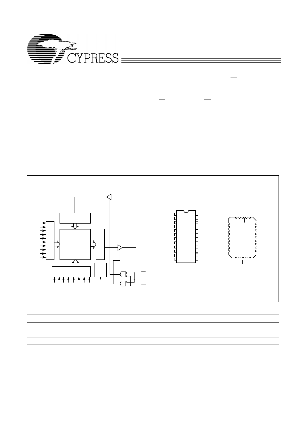
The CY7C197 is a high-performance CMOS stati c RAM organized as 256K words b y 1 bit. Easy memory ex pansion i s pro-
vided by an activ e LOW Chi p Enab le (CE
) and three-s tate drivers. The CY7C197 has an automatic power-down feature,
reducing the powe r consumption by 75% when desel ected.
Writing to the device is accomplished when the Chip Enable
(CE
) and Write Enab le (WE) input s are both LOW. Data on the
input pin (D
IN
) is written into the memory location spe cified on
the address pins (A
0
through A17).
Reading the device is accomplished by taking chip enable
(CE
) LOW while Write Enable (WE) remains HIGH. Under
these conditions the co ntents of the memory locat ion speci fied
on the address pins will appear on th e data outp ut (D
OUT
) pin.
The output pin stays in a high-impedance state when Chip
Enable (CE
) is HIGH or Write Enable (WE) is LOW.
The CY7C197 utilizes a die coat to insure alpha immunity.
WE
GND
28
LogicBlock Diagram Pin Configurations
1024 x256
ARRAY
A
1
A
2
A
3
A
4
A5A
6
A
7
A
8
COLUMN
DECODER
ROW DECODER
SENSE AMPS
POWER
DOWN
WE
CE
4
5
6
7
8
9
10
321 27
1314151617
26
25
24
23
22
21
20
1
2
3
4
5
6
7
8
9
10
11
14
15
16
20
19
18
17
21
24
23
22
Top View
DIP/SOJ
7C197
A
0
A
1
A
2
A
3
A
4
A
5
A
6
A
7
A
8
CE
V
CC
A
17
A
16
A
15
A
14
A
11
A
10
A
9
D
IN
A
13
A
12
D
OUT
11
12
19
18
A
2
V
CC
A
3
A
4
A
5
A
6
A
7
A
8
NC
A
9
GND
WE
7C197
Top View
LCC
12 13
INPUT BUFFER
DO
DI
A
0
A9A10A11A
12
A
17
A
16
A
15
A
14
A
13
CE
D
IN
A1A0A
17
NC
NCNC
D
OUT
A
16
A
15
A
14
A
11
A
10
A
13
A
12
C197-1
C197-2 C197-3
Selection Guid e
7C197-12 7C197-15 7C197-20 7C197-25 7C197-35 7C197-45
Maximum Access Time (ns) 12 15 20 25 35 45
Maximum Operating Curr ent (mA) 150 140 135 95 95
Maximum Standby Current (mA) 30 30 30 30 30 30
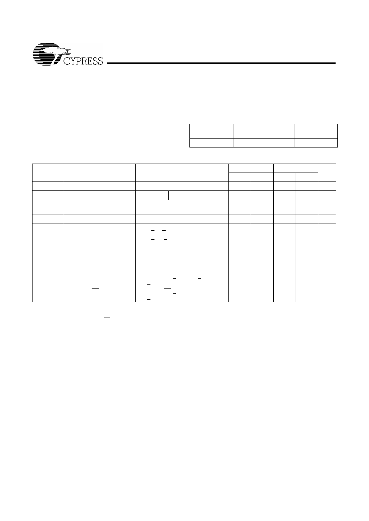
CY7C197
2
Maximum Ratings
(Above which the useful life may be impair ed. For user guidelines, not tested.)
Storage Temperature .....................................−65
°
C to +150°C
Ambient Temperature with
Po wer Applied..................................................−55
°
C to +125°C
Supply Voltage to Ground Potential
(Pin 24 to Pin 12).................................................−0.5V to +7.0V
DC V oltage Applied to Outputs
in High Z State
[1]
....................................... −0.5V to V
CC
+ 0.5V
DC Input Voltage
[1]
.................................... −0. 5V to V
CC
+ 0.5V
Output Current into Outputs (LOW)............................. 20 mA
Static Discharge Voltage .......... ............ ............ ........ >2001V
(per MIL-STD-883, Method 3015)
Latch-Up Current............. .. .......... .. .................... .. ... >200 mA
Operating Range
Range
Ambient
Temperature
V
CC
Commercial 0°C to +70°C 5V ± 10%
Electrical Characteristics
Over the Operating Range
Parameter Description Test Conditions
7C197-12 7C197-15
UnitMin. Max. Min. Max.
V
OH
Output HIGH Voltage VCC = Min., IOH = −4.0 mA 2.4 2.4 V
V
OL
Output LOW Voltage VCC = Min. IOL=12.0 mA 0.4 0.4 V
V
IH
Input HIGH Voltage 2.2 V
CC
+ 0.3V
2.2 V
CC
+0.3V
V
V
IL
Input LOW Voltage
[1]
−0.5 0.8 −0.5 0.8
V
I
IX
Input Load Current GND < VI < V
CC
−5+5−5+5µA
I
OZ
Output Leakage Current GND < VO < VCC, Output Disabled −5+5−5+5
µA
I
OS
Output Short
Circuit Current
[2]
VCC = Max., V
OUT
= GND −300 −300 mA
I
CC
VCC Oper ating
Supply Current
VCC = Max., I
OUT
= 0 mA,
f = f
MAX
= 1/t
RC
150 140 mA
I
SB1
Automati c C E Power-Down
Current—TTL Inputs
[3]
Max. VCC, CE > VIH, VIN > VIH or
V
IN
< VIL, f = f
MAX
30 30 mA
I
SB2
Automati c C E Power-Down
Current—CMOS Inputs
[3]
Max. VCC, CE > VCC − 0.3V,
V
IN
> VCC − 0.3V or VIN < 0.3V
10 10
mA
Notes:
1. V
(min.)
= −2.0V for pulse durations of less than 20 ns.
2. Not more than one output should be shorted at one time. Duration of the short circuit should not exceed 30 seconds.
3. A pull-up resistor to VCC on the CE input is required to keep the device deselected during VCC power-up, otherwise ISB will exceed values given.
CY7C197
3
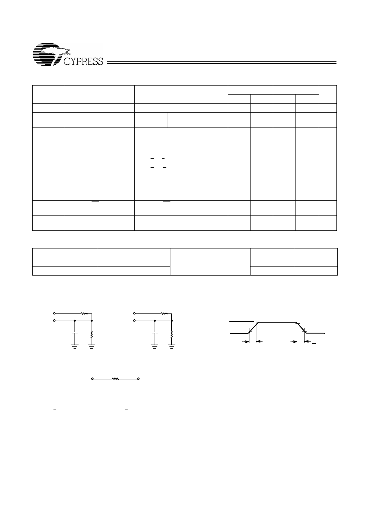
Electrical Characteristics
Over the Operating Range (conti nued)
Parameter Description T est Condi tions
7C197-20
7C197-25, 35, 45
UnitMin. Max. Min. Max.
V
OH
Output HIGH Voltage VCC = Min., IOH = −4.0 mA 2.4 2.4 V
V
OL
Output LOW Voltage VCC = Min. IOL= 12.0mA 0.4 0.4 V
V
IH
Input HIGH Voltage 2.2 V
CC
+ 0.3V
2.2 V
CC
+ 0.3V
V
V
IL
Input LOW Voltage
[1]
−0.5
0.8
−0.5
0.8 V
I
IX
Input Load Current GND < VI < V
CC
−5
+5
−5
+5
µA
I
OZ
Output Leakage Current GND < VO < VCC, Output Disabled
−5
+5
−5
+5
µA
I
OS
Output Short
Circuit Current
[2]
VCC = Max., V
OUT
= GND
−300 −300
mA
I
CC
VCC Oper ating
Supply Current
VCC = Max., I
OUT
= 0 mA,
f = f
MAX
= 1/t
RC
135 95 mA
I
SB1
Automatic CE Power Do wn
Current—TTL Inputs
[3]
Max. VCC, CE > VIH, VIN > VIH or
V
IN
< VIL, f = f
MAX
30 30 mA
I
SB2
Automatic CE Power -Down
Current—CMOS Inputs
[3]
Max. VCC, CE > VCC − 0.3V,
V
IN
> VCC − 0.3V or VIN < 0.3V
15 15 mA
Capacitance
[4]
Parameter Description Test Conditions Max. Unit
C
IN
Input Capacitance TA = 25°C, f = 1 MHz,
V
CC
= 5.0V
8 pF
C
OUT
Output Capacitance 10 pF
AC Test Loads and Waveforms
[5]
Notes:
4. Tested initially and after any design or process changes that may affect these parameters.
5. t
r
= < 3 ns for the -12 and -15 speeds. tr = < 5 ns for the -20 and slower speeds.
R2
255
Ω
(255ΩMIL)
R1 329
Ω
3.0V
5V
OUTPUT
R1 329
Ω
R2
202
Ω
(255ΩMIL)
30 pF
INCLUDING
JIG AND
SCOPE
GND
90%
10%
90%
10%
<t
r
<t
r
5V
OUTPUT
5pF
INCLUDING
JIG AND
SCOPE
(a) (b)
OUTPUT 1.90V
Equivalent to: THÉ VENIN EQUIVALENT
Commercial
ALL INPUT PULSES
C197-4
C197-5
125
Ω
 Loading...