

Datasheet CY7C187-35VCT, CY7C187-35VC, CY7C187-35PC, CY7C187-25VCT, CY7C187-25VC Datasheet (Cypress Semiconductor)
...
64K x 1 Static RAM
CY7C187
Cypress Semiconductor Corporation
• 3901 North First Street • San Jose • CA 95134 • 408-943-2600
October 4, 1999
Features
• High speed
—15 ns
• CMOS for optimum speed/power
• Low active power
—495 mW
• Low standb y p ow er
—220 mW
• TTL compatible inputs and outputs
• Automat ic power-down when deselected
Functional Description
The CY7C187 is a high-performance CMOS stati c RAM organized as 65, 536 words x 1 bit. Eas y memory expa nsi on is pr o-
vided by an activ e LOW Chi p Enab le (CE
) and three-s tate drivers. The CY7C187 has an automatic power-down feature,
reducing the powe r consumption by 56% when desel ected.
Writing to the device is accomplished when the Chip Enable
(CE
) and Write Enab le (WE) input s are both LOW. Data on the
input pin (D
IN
) is written into the memory location spe cified on
the address pins (A
0
through A15).
Reading the devi ce is accompl ished by ta king the Chip Enab le
(CE
) LOW, while Write Enable (WE) remains HIGH. Under
these conditions, the contents of the memory location specified on the address pin will appear on the data output (D
OUT
)
pin.
The output pin stays in high-impedance state when Chip En-
able (CE
) is HIGH or W r ite E nabl e ( WE) is LOW.
The CY7C187 utilizes a die coat to insure alpha imm unity.
Logic Block Diagram Pin Configurations
256x 256
ARRAY
C187–1
A
12
A
13
A
14
A
15
A
0
A
1
A
2
A
3
A4A
5
A10A
11
COLUMN DECODER
ROW DECODER
SENSE AMPS
INPUT BUFFER
POWER
DOWN
DI
DO
CE
WE
A7A
6
A9A
8
1
2
3
4
5
6
7
8
9
10
11 12
13
14
18
17
16
15
19
22
21
20
Top View
DIP
A
0
A
1
A
2
A
3
A
4
D
OUT
WE
GND
CE
V
CC
A
15
A
14
A
13
A
12
A
10
A
9
A
8
D
IN
A
11
C187–2
WE
1
2
3
4
5
6
7
8
9
10
11
14
15
16
20
19
18
17
21
24
23
22
Top View
SOJ
A
0
A
1
A
2
A
3
A
4
NC
CE
V
CC
A
15
A
14
A
13
A
12
A
10
A
9
A
8
D
IN
NC
GND
D
OUT
12 13
C187–3
A
5
A
6
A
7
A
11
A
5
A
6
A
7
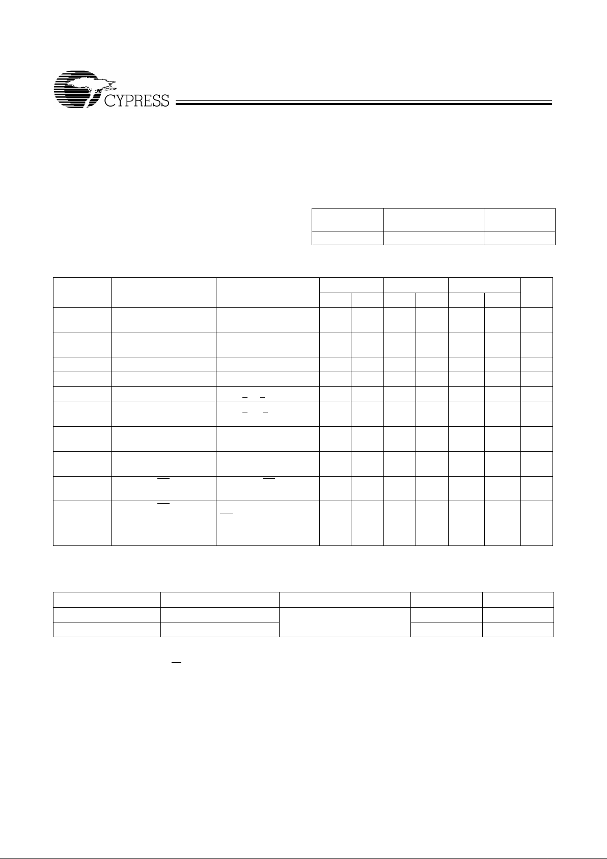
Selection Guid e
[1]
7C187-15 7C187-20 7C187-25 7C187-35
Maximum Access Time (ns) 15 20 25 35
Maximum Operating Curr ent (mA) 90 80 70 70
Maximum Standby Current (mA) 40/20 40/20 20/20 20/20
Note:
1. For military specifications, see the CY7C187A datasheet.
CY7C187
2
Maximum Ratings
(Above which the useful life may be impaired. For use r gui delines, not tested.)
Storage Temperature ......................... .. ......–65°C to +150°C
Ambient Temperature with
Power Applied.............................................–55°C to +125°C
Supply Voltage to Ground Potential
(Pin 22 to Pi n 11 ) ........ ... .. .............................. –0.5V to +7.0V
DC V oltage Applied to Outputs
in High Z State
[2]
............................................ –0.5V to +7.0V
DC Input Voltage
[2]
.........................................–0.5V to +7. 0V
Output Current into Outputs (LOW)............................. 20 mA
Static Discharge Voltage .......... ............ ............ .........>2001V
(per MIL–STD–883, Method 3015)
Latch-Up Current .....................................................>200 mA
Operating Range
Range
Ambient
Temperature V
CC
Commercial 0°C to +70°C 5V ± 10%
Electrical Characteristics
Over the Operating Range
7C187-15 7C187-20 7C187-25, 35
Parameter Description Test Conditions Min. Max. Min. Max. Min. Max. Unit
V
OH
Output HIGH Voltage VCC = Min.,
I
OH
= –4.0 mA
2.4 2.4 2.4 V
V
OL
Output LOW Voltage VCC = Min.,
I
OL
=1 2.0 mA
0.4 0.4 0.4 V
V
IH
Input HIGH Voltage 2.2 V
CC
2.2 V
CC
2.2 V
CC
V
V
IL
Input LOW Voltage
[2]
–0.5 0.8 –0.5 0.8 –0.5 0.8 V
I
IX
Input Load Current GND < VI < V
CC
–5 +5 –5 +5 –5 +5
µA
I
OZ
Output Leakage
Current
GND < V
O
<
VCC,
Output Disabled
–5 +5 –5 +5 –5 +5
µA
I
OS
Output Short
Circuit Current
[3]
VCC = Max.,
V
OUT
= GND
–350 –350 –350 mA
I
CC
VCC Operating
Supply Current
VCC = Max.,
I
OUT
= 0 mA
90 80 70 mA
I
SB1
Automati c C E PowerDown Current
[4]
Max. VCC, CE ≥ V
IH
40 40 20 mA
I
SB2
Automati c C E
Po wer-Down Current
Max. VCC,
CE
≥ VCC – 0.3V,
V
IN
≥ VCC – 0.3V
or V
IN
≤ 0.3V
20 20 20 mA
Capacitance
[5]
Parameter Description Test Conditions Max. Unit
C
IN
Input Capacitance TA = 25°C, f = 1 MH z,
V
CC
= 5.0V
10 pF
C
OUT
Output Capacitance 10 pF
Notes:
2. V
IL
(min.) = –3.0V for pulse durations less than 30 ns.
3. Not more than 1 output should be shorted at one time. Duration of the short circuit should not exceed 30 seconds.
4. A pull-up resistor to VCC on the CE input is required to keep the device deselected during VCC power-up, otherwise ISB will exceed values given.
5. Tested initially and after any design or process changes that may affect these parameters.

CY7C187
3
AC Test Loads and Waveforms
(R1 255ΩMIL)
(R1 255ΩMIL)
(480ΩMIL) (480
Ω
MIL)
3.0V
5V
OUTPUT
R1 329
Ω
R2 202
Ω
30 pF
GND
90%
90%
10%
≤
5ns
≤
5
ns
5V
OUTPUT
C187–4
R2 202
Ω
5
pF
C187–5
(a) (b)
OUTPUT 1.73V
INCLUDING
JIG AND
SCOPE
INCLUDING
JIG AND
SCOPE
R1 329
Ω
Equivalentto: THÉ VENIN EQUIVALENT
10%
OUTPUT 1.90V
Military Commercial
ALL INPUT PULSES
167
Ω
125
Ω
Switching Characteristics
Over the Operating Range
[6]
7C187-15 7C187-20
Parameter Description Min. Max. Min. Max. Unit
READ CYCLE
t
RC
Read Cycle Time 15 20 ns
t
AA
Address to Data Valid 15 20 ns
t
OHA
Output Hold from Address Change 3 5 ns
t
ACE
CE LOW to Data Valid 15 20 ns
t
LZCE
CE LOW to Low Z
[7]
3 5 ns
t
HZCE
CE HIGH to High Z
[7, 8]
8 8 ns
t
PU
CE LOW to Power Up 0 0 ns
t
PD
CE HIGH to Powe r Down 15 20 ns
WRITE CYCLE
[9]
t
WC
Write Cycle Time 15 20 ns
t
SCE
CE LOW to Write End 12 15 ns
t
AW
Address Set-Up to Write End 12 15 ns
t
HA
Address Hold from Write End 0 0 ns
t
SA
Address Set-Up to Write Start 0 0 ns
t
PWE
WE Pulse Width 12 15 ns
t
SD
Data Set-Up to Write End 10 10 ns
t
HD
Data Hold from Write End 0 0 ns
t
LZWE
WE HIGH to Low Z 5 5 ns
t
HZWE
WE LOW to High Z
[8]
7 7 ns
Notes:
6. Tes t conditions assume signal transition time of 5 ns or less, timing reference levels of 1.5V , input pulse levels of 0 to 3.0V , and output loading of the specified
I
OL/IOH
and 30-pF load capacitance.
7. At any given temperature and voltage condition, t
HZCE
is less than t
LZCE
for any given device.
8. t
HZCE
and t
HZWE
are specified with CL = 5 pF as in part (b) of AC Test Loads. Transition is measured ±500 mV from steady-state voltage.
9. The internal write time of the memory is defined by the overlap of CE
LOW and WE LOW. Both signals must be LOW to initiate a write and either signal can
terminate a write by going HIGH. The data input set-up and hold timing should be referenced to the rising edge of the signal that terminates the write.

CY7C187
4
Switching Characteristics
Over the Operating Range
[6]
(continued)
7C187-25 7C187-35
Parameters Description Min. Max. Min. Max. Units
READ CYCLE
t
RC
Read Cycle Time 25 35 ns
t
AA
Address to Data Valid 25 35 ns
t
OHA
Output Hold from Address Change 5 5 ns
t
ACE
CE LOW to Data Valid 25 35 ns
t
LZCE
CE LOW to Low Z
[7]
5 5 ns
t
HZCE
CE HIGH to High Z
[7, 8]
10 15 ns
t
PU
CE LOW to Po wer Up 0 0 ns
t
PD
CE HIGH to Power Down 20 20 ns
WRITE CYCLE
[9]
t
WC
Write Cycle Time 20 25 ns
t
SCE
CE LOW to Write End 20 25 ns
t
AW
Address Set-Up to Write End 20 25 ns
t
HA
Address Hold from Write End 0 0 ns
t
SA
Address Set-Up to Write Start 0 0 ns
t
PWE
WE Pulse Widt h 15 20 ns
t
SD
Data Se t- U p to Wr ite End 10 15 ns
t
HD
Data Hold from Write End 0 0 ns
t
LZWE
WE HIGH to Low 5 5 ns
t
HZWE
WE LOW to High Z
[8]
7 10 ns
Switching Waveforms
Read Cycle No. 1
[10, 11]
Notes:
10. WE
is HIGH for read cycle.
11. Device is continuously selected, CE = VIL.
ADDRESS
DATA OUT PREVIOUS DATA VALID
DATA VALID
t
RC
t
AA
t
OHA
C187–6

CY7C187
5
Read Cycle No. 2
[10, 12]
Notes:
12. Address valid prior to or coincident with CE
transition LOW.
13. If CE goes HIGH simultaneously with WE HIGH, the output remains in a high-impedance state.
Switching Waveforms
50%
50%
DATA VALID
t
RC
t
ACE
t
LZCE
t
PU
DATA OUT
HIGH IMPEDANCE
IMPEDANCE
ICC
ISB
t
HZCE
t
PD
CE
HIGH
t
WC
DATA VALID
DATA UNDEFINED
HIGH IMPEDANCE
t
SCE
t
AW
t
SA
t
PWE
t
HA
t
HD
V
CC
SUPPLY
CURRENT
t
HZWE
t
LZWE
t
SD
CE
WE
DATA IN
DATA OUT
ADDRESS
C187–7
C187–8
t
WC
DATA VALID
HIGH IMPEDANCE
t
SCE
t
AW
t
SA
t
PWE
t
HA
t
HD
t
SD
CE
WE
ADDRESS
DATA IN
DATA OUT
C187–9
Write Cycle No. 1 (WE Co ntrolled)
[11]
Write Cycle No. 2 (CE Controlled)
[11, 13]

CY7C187
6
T y pical DC and AC Characteris ti cs
1.2
1.4
1.0
0.6
0.4
0.2
4.0 4.5 5.0 5.5 6.0
1.6
1.4
1.2
1.0
0.8
–55 25 125
–55 25 125
1.2
1.0
0.8
NORMALIZED t
AA
120
100
80
60
40
20
0.0 1.0 2.0 3.0 4.0
OUTPUT SOURCE CURRENT (mA)
SUPPLY VOLTAGE(V)
NORMALIZED SUPPLY CURRENT
vs. SUPPLY VOLTAGE
NORMALIZED ACCESS TIME
vs. AMBIENT TEMPERATURE
AMBIENT TEMPERATURE (°C)
NORMALIZED SUPPLY CURREN T
vs. AMBIENT TEMPERATURE
AMBIENT TEMPERATURE (°C)
OUTPUT VOLTAGE (V)
OUTPUT SOURCE CURRENT
vs. OUTPUT
VOLTAGE
0.0
0.8
1.4
1.3
1.2
1.1
1.0
0.9
4.0 4.5 5.0 5.5 6.0
NORMALIZED t
AA
SUPPLY VOLTAGE (V)
NORMALIZED ACCESS TIME
vs. SUPPLY
VOLTAGE
120
140
100
60
40
20
0.0 1.0 2.0 3.0 4.0
OUTPUT SINK CURRENT (mA)
0
80
OUTPUT VOLTAGE (V)
OUTPUT SINKCURRE NT
vs. OUTPUT VOLTAGE
0.6
0.4
0.2
0.0
NORMALIZED I
CC, SB
NORMALIZED I
CC, SB
I
SB
VCC=5.0V
V
IN
=5.0V
I
CC
I
CC
VCC=5.0V
V
CC
=5.0V
T
A
=25°C
V
CC
=5.0V
T
A
=25°C
I
SB
TA=25°C
0.6
0.8
0
I
I
3.0
2.5
2.0
1.5
1.0
0.5
0.0 1.0 2.0 3.0 4.0
NORMALIZED I
PO
SUPPLY VOLTAGE(V)
TYPICAL POWER-ON CURRENT
vs. SUPPLY
VOLTAGE
30.0
25.0
20.0
15.0
10.0
5.0
0 200 400 600 800
NORMALIZED t (ns)
AA
CAPACITANCE (pF)
TYPICAL ACCESS TIME CHANGE
vs. OUTPUT
LOADING
1.25
1.00
0.75
10 20 30 40
NORMALIZED I
CC
CYCLE FREQUENCY (MHz)
NORMALIZED I
CC
vs.CYCLE TIME
0.0
5.0
0.0
1000
0.50
V
CC
=4.5V
T
A
=25°C
V
CC
=5.0V
T
A
=25°C
V
CC
=0.5V

CY7C187
7
Document #: 38–00038–K
Address Designators
Address
Name
Address
Function
Pin
Number
A0 X3 1
A1 X4 2
A2 X5 3
A3 X6 4
A4 X7 5
A5 Y7 6
A6 Y6 7
A7 Y2 8
A8 Y3 14
A9 Y1 15
A10 Y0 16
A11 Y4 17
A12 Y5 18
A13 X0 19
A14 X1 20
A15 X2 21
T ruth T a ble
CE WE Input/Output Mode
H X High Z Deselect/Power-Down
L H Data Out Read
L L Data In Write
Ordering Information
[14]
Speed
(ns) Ordering Code
Package
Name
Package
Type
Operating
Range
15 CY7C187-15PC P9 22-Lead (300-Mil) Molded DIP Commercial
CY7C187-15VC V13 24-Lead Molded SOJ
20 CY7C187-20PC P9 22-Lead (300-Mil) Molded DIP Commercial
CY7C187-20VC V13 24-Lead Molded SOJ
25 CY7C187-25PC P9 22-Lead (300-Mil) Molded DIP Commercial
CY7C187-25VC V13 24-Lead Molded SOJ
35 CY7C187-35PC P9 22-Lead (300-Mil) Molded DIP Commercial
CY7C187-35VC V13 24-Lead Molded SOJ
Note:
14. For military variations, see the CY7C187A datasheet.

CY7C187
© Cypress Semiconductor Corporation, 1999. The information contained herein is subject to change without notice. Cypress Semiconductor Corporation assumes no responsibility for the use
of any circuitry other than circuitry embodied in a Cypress Semiconductor product. Nor does it con vey or imply any license under patent or other rights. Cypress Semiconductor does not authorize
its products for use as critical components in life-support systems where a malfunction or failure may reasonably be expected to result in significant injury to the user. The inclusion of Cypress
Semiconductor products in life-support systems application implies that the manufacturer assumes all risk of such use and in doing so indemnifies Cypress Semiconductor against all charges.
Package Diagrams
51-85012-A
22-Lead(300-Mil)Molded DIP P9
24-Lead (300-Mil) Molded SOJ V13
51-85030-A
 Loading...