

Cypress Semiconductor CY7C168A-45PC, CY7C168A-45DMB, CY7C168A-35VC, CY7C168A-35PC, CY7C168A-35DMB Datasheet
...
4Kx4 RAM
CY7C168A
Cypress Semiconductor Corporation
• 3901 North First Street • San Jose • CA 95134 • 408-943-2600
February 3, 2000
Features
• Automat ic power-down when deselected
• CMOS for optimum speed/power
• High speed
—t
AA
= 15 ns
• Low active power
—633 mW
• Low standb y p ow er
—110 mW
• TTL-compatibl e inputs and outputs
•V
IH
of 2.2V
• Capable of wit hstanding greater than 200 1V electrostat-
ic discharge
Functional Description
The CY7C168A is a high-performance CMOS static RAM organized as 4096 b y 4 bits. Easy memory e xpansion is provi ded
by an active LOW Chip Enable (CE
) and three-state drivers.
The CY7C168A has an au tomatic po wer -down f eatur e, r educing the power consumption by 77% when deselected.
Writing to the device is accomplished when the Chip Select
(CE
) and Write Enab le (WE) input s are both LOW. Data on the
four data input/ output pins (I/O
0
through I/O3) is written into the
memory location specified on the address pins (A
0
through
A
11
).
Reading the devi ce is accompl ished by ta king the Chip Enab le
(CE
) LOW, while Write Enable (WE) remains HIGH. Under
these conditions, the contents of the location specified on the
address pins will appear on the four data input/output pins
(I/O
0
through I/O3).
The input/output pins remain in a high-impedance state when
Chip E nable (C E
) is HIGH or Wr i te Enabl e (WE ) is LOW.
A die coat is used to insure alpha immunity.
Logic Block Diagram Pin Configurations
128x 128
ARRAY
C168A-1
1
2
3
4
5
6
7
8
9
10 11
12
13
14
18
17
16
15
Top View
DIP/SOJ
7C168A
A
1
A
2
A
3
A
8
A
9
A
4
A
0
COLUMN
DECODER
ROW DECODER
SENSE AMP
INPUTBUFFER
POWER
DOWN
WE
CE
I/O
0
A
5
A
6
A
7
A
8
A
9
A
11
WE
GND
CE
V
CC
A
2
A
1
A
0
C168A-2
I/O
1
A10A
11
A
5
A
4
I/O
0
I/O
1
I/O
2
I/O
3
I/O
2
I/O
3
A
7
A
6
A
10
A
3
(7C168A)
20
19
\
Selection Guid e
7C168A-15 7C168A-20 7C168A-25 7C168A-35 7C168A-45
Maximum Access Time (ns) 15 20 25 35 45
Maximum Operating
Current (mA)
Commercial 115 90 90 90 90
Military - 100 100 100 100
CY7C168A
2
Maximum Ratings
(Above which the useful lif e m ay be impaired. For user guidelines, not tested.)
Storage Temperature .....................................−65°C to +150°C
Ambient Temperature with
Po wer Applied..................................................−55°C to +12 5 °C
Supply Voltage to Ground Potential
(Pin 20 to Pin 10)................................................ −0.5V to +7.0V
DC V oltage Applied to Outputs
in High Z State.................................................... −0.5V to +7.0V
DC Input Voltage.................................................−3.0V to +7.0V
Output Current into Outputs (Low) .............................. 20 mA
Static Discharge Voltage .......... ......................... .. ......>2001V
(per MIL-STD-883, Method 3015)
Latch-Up Current.....................................................>200 mA
Operating Range
Range
Ambient
Temperature
V
CC
Commercial 0°C to +70°C 5V ± 10%
Military
[1]
−55°
C to +125°C 5V ± 10%
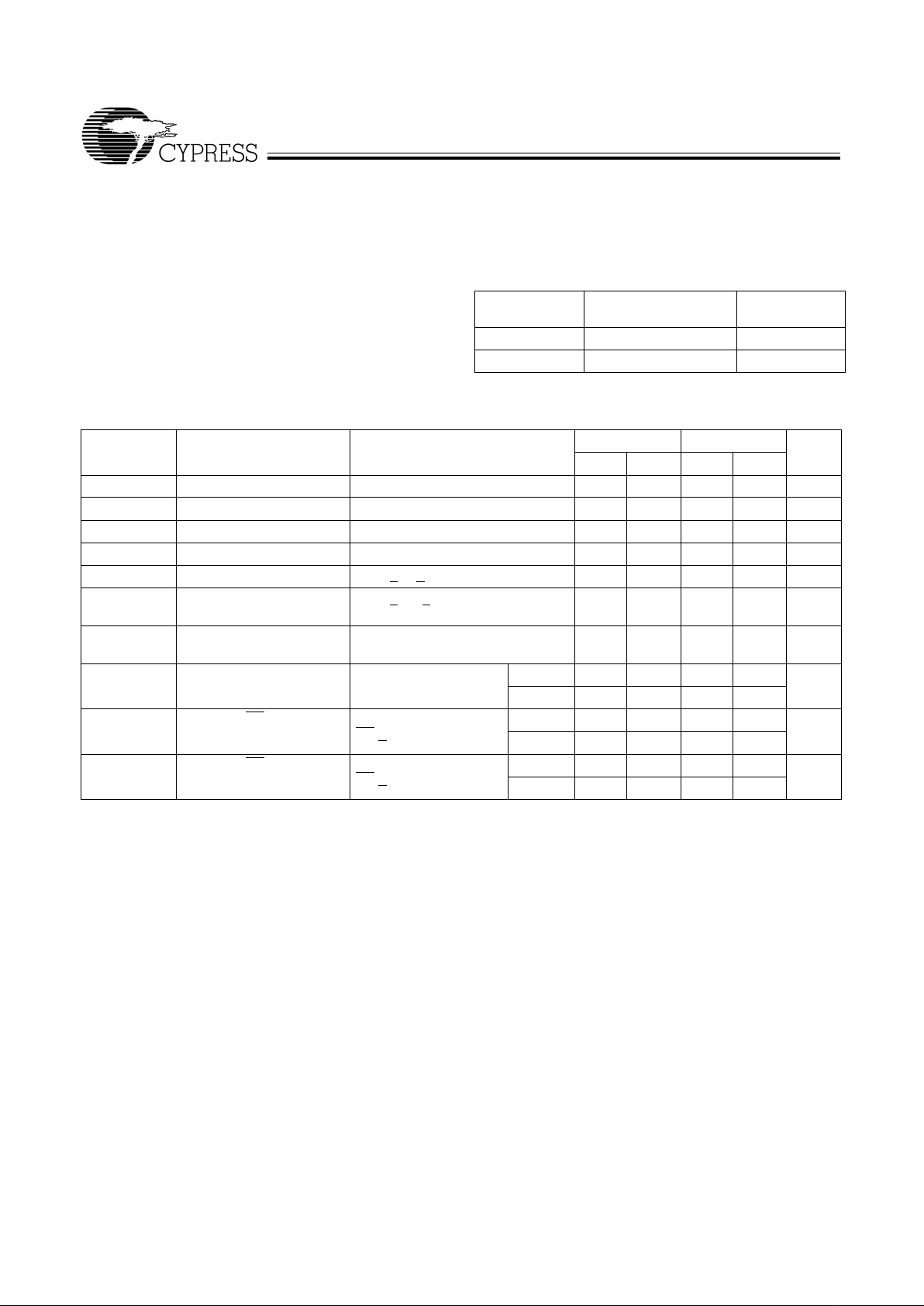
Electrical Characteristics
Over the Operating Range
[2]
7C168A-15 7C168A-20
Parameter Description Tes t Condi ti ons Min. Max. Min. Max. Unit
V
OH
Output HIGH Voltage VCC = Min., IOH = −4.0 mA 2.4 2.4 V
V
OL
Output LOW Vol tage VCC = Min., I
OL
= 8.0 mA 0.4 0.4 V
V
IH
Input HIGH Voltage 2.2 V
CC
2.2 V
CC
V
V
IL
Input LOW Voltage
[3]
−0.5
0.8
−0.5
0.8 V
I
IX
Input Load Current GND < VI < V
CC
−10
+10
−10
+10
µA
I
OZ
Output Leakage
Current
GND < VO < VCC,
Output Disabled
−10
+10
−10
+10
µA
I
OS
Output Short
Circuit Current
[4]
VCC = Max., V
OUT
= GND
−350 −350
mA
I
CC
VCC Oper ating
Supply Current
V
CC =
Max.,
I
OUT
= 0 mA
Com’l 115 90 mA
Mil - 100
I
SB1
Automati c C E
Po wer-Down Current
Max. VCC,
CE
> V
IH
Com’l 40 40 mA
Mil - 40
I
SB2
Automati c C E
Po wer-Down Current
Max. VCC,
CE
> VCC − 0.3V
Com’l 20 20 mA
Mil - 20
Notes:
1. T
A
is the “instant on” case temperature.
2. See the last page of this specification for Group A subgroup testing information.
3. V
IL
min. = −3.0V for pulse durations less than 30 ns.
4. Not more than 1 output should be shorted at one time. Duration of the short circuit should not exceed 30 seconds.

CY7C168A
3
Electrical Characteristics
Over the Operating Range
[2]
(continued)
Parameter Description Test Conditions
7C168A-25 7C168A-35 7C168A-45
Min. Max. Min. Max. Min. Max. Unit
V
OH
Outp ut HIGH Voltage VCC = Min., IOH = −4.0 mA 2.4 2.4 2.4 V
V
OL
Output LOW Voltage VCC = Min., I
OL
= 8.0 mA 0.4 0.4 0.4 V
V
IH
Input HIGH Voltage 2.2 V
CC
2.2 V
CC
2.2 V
CC
V
V
IL
Input LOW Voltage
[3]
−0.5
0.8
−0.5
0.8
−0.5
0.8 V
I
IX
Input Load Current GND < VI < V
CC
−10
+10
−10
10
−10
10
µA
I
OZ
Output Leakage
Current
GND < VO < V
CC
Output Disabled
−10
+10
−50
50
−50
50
µA
I
OS
Output Short
Circuit Current
[4]
VCC = Max., V
OUT
= GND
−350 −350 −350
mA
I
CC
VCC Operating
Supply Current
V
CC =
Max.,
I
OUT
= 0 mA
Com’l 90 90 90 mA
Mil 100 100 100
I
SB1
Auto mati c CE
Power-Down Current
Max. VCC,
CE
> V
IH
Com’l 20 20 20 mA
Mil 20 20 20
I
SB2
Auto mati c CE
Power-Down Current
Max. VCC,
CE
> VCC − 0.3 V
Com’l 20 20 20 mA
Mil 20 20 20
Capacitance
[5]
Parameter Description Test Conditions Max. Unit
C
IN
Input Capacitance TA = 25°C, f = 1 MH z,
V
CC
= 5.0V
10 pF
C
OUT
Output Capacitance 10 pF
Note:
5. Tested initially and after any design or process changes that may affect these parameters.
AC Test Loads and Waveforms
3.0V
5V
OUTPUT
R1 481
Ω
R2
255
Ω
30pF
INCLUDING
JIG AND
SCOPE
GND
90%
10%
90%
10%
<5ns
< 5 ns
5V
OUTPUT
C168A-3
R1 481
Ω
R2
255
Ω
5pF
INCLUDING
JIG AND
SCOPE
C168A-4
(a) (b)
OUTPUT 1.73V
Equivalent to: THÉ VENIN EQUIVALENT
ALL INPUT PULSES
167
Ω
 Loading...