

Cypress Semiconductor CY7C168A-45PC, CY7C168A-45DMB, CY7C168A-35VC, CY7C168A-35PC, CY7C168A-35DMB Datasheet
...
4Kx4 RAM
CY7C168A
Cypress Semiconductor Corporation
• 3901 North First Street • San Jose • CA 95134 • 408-943-2600
February 3, 2000
Features
• Automat ic power-down when deselected
• CMOS for optimum speed/power
• High speed
—t
AA
= 15 ns
• Low active power
—633 mW
• Low standb y p ow er
—110 mW
• TTL-compatibl e inputs and outputs
•V
IH
of 2.2V
• Capable of wit hstanding greater than 200 1V electrostat-
ic discharge
Functional Description
The CY7C168A is a high-performance CMOS static RAM organized as 4096 b y 4 bits. Easy memory e xpansion is provi ded
by an active LOW Chip Enable (CE
) and three-state drivers.
The CY7C168A has an au tomatic po wer -down f eatur e, r educing the power consumption by 77% when deselected.
Writing to the device is accomplished when the Chip Select
(CE
) and Write Enab le (WE) input s are both LOW. Data on the
four data input/ output pins (I/O
0
through I/O3) is written into the
memory location specified on the address pins (A
0
through
A
11
).
Reading the devi ce is accompl ished by ta king the Chip Enab le
(CE
) LOW, while Write Enable (WE) remains HIGH. Under
these conditions, the contents of the location specified on the
address pins will appear on the four data input/output pins
(I/O
0
through I/O3).
The input/output pins remain in a high-impedance state when
Chip E nable (C E
) is HIGH or Wr i te Enabl e (WE ) is LOW.
A die coat is used to insure alpha immunity.
Logic Block Diagram Pin Configurations
128x 128
ARRAY
C168A-1
1
2
3
4
5
6
7
8
9
10 11
12
13
14
18
17
16
15
Top View
DIP/SOJ
7C168A
A
1
A
2
A
3
A
8
A
9
A
4
A
0
COLUMN
DECODER
ROW DECODER
SENSE AMP
INPUTBUFFER
POWER
DOWN
WE
CE
I/O
0
A
5
A
6
A
7
A
8
A
9
A
11
WE
GND
CE
V
CC
A
2
A
1
A
0
C168A-2
I/O
1
A10A
11
A
5
A
4
I/O
0
I/O
1
I/O
2
I/O
3
I/O
2
I/O
3
A
7
A
6
A
10
A
3
(7C168A)
20
19
\
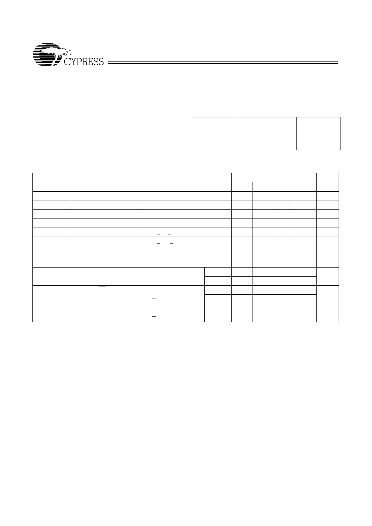
Selection Guid e
7C168A-15 7C168A-20 7C168A-25 7C168A-35 7C168A-45
Maximum Access Time (ns) 15 20 25 35 45
Maximum Operating
Current (mA)
Commercial 115 90 90 90 90
Military - 100 100 100 100
CY7C168A
2
Maximum Ratings
(Above which the useful lif e m ay be impaired. For user guidelines, not tested.)
Storage Temperature .....................................−65°C to +150°C
Ambient Temperature with
Po wer Applied..................................................−55°C to +12 5 °C
Supply Voltage to Ground Potential
(Pin 20 to Pin 10)................................................ −0.5V to +7.0V
DC V oltage Applied to Outputs
in High Z State.................................................... −0.5V to +7.0V
DC Input Voltage.................................................−3.0V to +7.0V
Output Current into Outputs (Low) .............................. 20 mA
Static Discharge Voltage .......... ......................... .. ......>2001V
(per MIL-STD-883, Method 3015)
Latch-Up Current.....................................................>200 mA
Operating Range
Range
Ambient
Temperature
V
CC
Commercial 0°C to +70°C 5V ± 10%
Military
[1]
−55°
C to +125°C 5V ± 10%
Electrical Characteristics
Over the Operating Range
[2]
7C168A-15 7C168A-20
Parameter Description Tes t Condi ti ons Min. Max. Min. Max. Unit
V
OH
Output HIGH Voltage VCC = Min., IOH = −4.0 mA 2.4 2.4 V
V
OL
Output LOW Vol tage VCC = Min., I
OL
= 8.0 mA 0.4 0.4 V
V
IH
Input HIGH Voltage 2.2 V
CC
2.2 V
CC
V
V
IL
Input LOW Voltage
[3]
−0.5
0.8
−0.5
0.8 V
I
IX
Input Load Current GND < VI < V
CC
−10
+10
−10
+10
µA
I
OZ
Output Leakage
Current
GND < VO < VCC,
Output Disabled
−10
+10
−10
+10
µA
I
OS
Output Short
Circuit Current
[4]
VCC = Max., V
OUT
= GND
−350 −350
mA
I
CC
VCC Oper ating
Supply Current
V
CC =
Max.,
I
OUT
= 0 mA
Com’l 115 90 mA
Mil - 100
I
SB1
Automati c C E
Po wer-Down Current
Max. VCC,
CE
> V
IH
Com’l 40 40 mA
Mil - 40
I
SB2
Automati c C E
Po wer-Down Current
Max. VCC,
CE
> VCC − 0.3V
Com’l 20 20 mA
Mil - 20
Notes:
1. T
A
is the “instant on” case temperature.
2. See the last page of this specification for Group A subgroup testing information.
3. V
IL
min. = −3.0V for pulse durations less than 30 ns.
4. Not more than 1 output should be shorted at one time. Duration of the short circuit should not exceed 30 seconds.

CY7C168A
3
Electrical Characteristics
Over the Operating Range
[2]
(continued)
Parameter Description Test Conditions
7C168A-25 7C168A-35 7C168A-45
Min. Max. Min. Max. Min. Max. Unit
V
OH
Outp ut HIGH Voltage VCC = Min., IOH = −4.0 mA 2.4 2.4 2.4 V
V
OL
Output LOW Voltage VCC = Min., I
OL
= 8.0 mA 0.4 0.4 0.4 V
V
IH
Input HIGH Voltage 2.2 V
CC
2.2 V
CC
2.2 V
CC
V
V
IL
Input LOW Voltage
[3]
−0.5
0.8
−0.5
0.8
−0.5
0.8 V
I
IX
Input Load Current GND < VI < V
CC
−10
+10
−10
10
−10
10
µA
I
OZ
Output Leakage
Current
GND < VO < V
CC
Output Disabled
−10
+10
−50
50
−50
50
µA
I
OS
Output Short
Circuit Current
[4]
VCC = Max., V
OUT
= GND
−350 −350 −350
mA
I
CC
VCC Operating
Supply Current
V
CC =
Max.,
I
OUT
= 0 mA
Com’l 90 90 90 mA
Mil 100 100 100
I
SB1
Auto mati c CE
Power-Down Current
Max. VCC,
CE
> V
IH
Com’l 20 20 20 mA
Mil 20 20 20
I
SB2
Auto mati c CE
Power-Down Current
Max. VCC,
CE
> VCC − 0.3 V
Com’l 20 20 20 mA
Mil 20 20 20
Capacitance
[5]
Parameter Description Test Conditions Max. Unit
C
IN
Input Capacitance TA = 25°C, f = 1 MH z,
V
CC
= 5.0V
10 pF
C
OUT
Output Capacitance 10 pF
Note:
5. Tested initially and after any design or process changes that may affect these parameters.
AC Test Loads and Waveforms
3.0V
5V
OUTPUT
R1 481
Ω
R2
255
Ω
30pF
INCLUDING
JIG AND
SCOPE
GND
90%
10%
90%
10%
<5ns
< 5 ns
5V
OUTPUT
C168A-3
R1 481
Ω
R2
255
Ω
5pF
INCLUDING
JIG AND
SCOPE
C168A-4
(a) (b)
OUTPUT 1.73V
Equivalent to: THÉ VENIN EQUIVALENT
ALL INPUT PULSES
167
Ω

CY7C168A
4
Switching Characteristics
Over the Operating Range
[2,6]
Parameter Description
7C168A-15 7C168A-20 7C168A-25 7C168A-35 7C168A-45
UnitMin. Max. Min. Max. Min. Max. Min. Max. Min. Max.
READ CYCLE
t
RC
Read Cycle Time 15 20 25 35 45 ns
t
AA
Address to Data Valid 15 20 25 35 45 ns
t
OHA
Output Hold f rom Address Cha nge 5 5 5 5 5 ns
t
ACE
Power Supply Current 15 20 25 35 45 ns
t
LZCE
CE LOW to Low Z
[7]
5 5 5 5 5 ns
t
HZCE
CE HIGH to High Z
[7, 8]
8 8 10 15 15 ns
t
PU
CE LOW to Power Up 0 0 0 0 0 ns
t
PD
CE HIGH to Power-Do wn 15 20 20 20 25 ns
t
RCS
Read Command Set-Up 0 0 0 0 0 ns
t
RCH
Read Command Hold 0 0 0 0 0 ns
WRITE CYCLE
[9]
t
WC
Write Cycle Time 15 20 20 25 40 ns
t
SCE
CE LOW to Write End 12 15 20 25 30 ns
t
AW
Address Set-Up to Write End 12 15 20 25 30 ns
t
HA
Address Hold from Write End 0 0 0 0 0 ns
t
SA
Address Set-Up to Write Start 0 0 0 0 0 ns
t
PWE
WE Pulse Width 12 15 15 20 20 ns
t
SD
Data Set-Up to Write End 10 10 10 15 15 ns
t
HD
Data Hold from Write End 0 0 0 0 0 ns
t
LZWE
WE HIGH to Low Z
[7]
7 7 7 5 5 ns
t
HZWE
WE LOW to High Z
[7, 8]
5 5 5 5 10 ns
Switching Waveforms
Notes:
6. Test conditions assume signal transition times of 5 ns or less, timing reference levels of 1.5V, input pulse levels of 0 to 3.0V, and output loading of the specified
I
OL/IOH
and 30-pF load capac itance.
7. At any given temperature and voltage condition, t
HZ
is less than tLZ for all d e vices. Transition is measured ±500 mV from stea dy state voltage with specified loading in part
(b) of AC Test Loads and Wa vef orms .
8. t
HZCE
and t
HZWE
are tested with CL = 5 pF as in pa rt (a) of Test Loads and Wa v ef orms . Transition is measured ±500 mV from steady state v oltag e.
9. The internal write time of the memory is defined by the overlap of CE
LOW and WE LO W. Both signal must be LO W to ini tiat e a w rite and either s ignal c an te rminate a
write by going high. Th e data input set- up a nd hold t imin g should be ref e renced to th e rising edge of th e si gnal that terminate s the write.
10. WE is HIGH f or read cycle.
11. Device is continuously selected, CE = VIL.
ReadCycle No. 1
ADDRESS
C168A-5
DATA OUT PREVIOUS DATA VALID DATA VALID
t
RC
t
AA
t
OHA
[10, 11]

CY7C168A
5
Notes:
12. Address valid prior to or coincident with CE
transition LO W.
13. If CE goe s HIGH s imultan eousl y with W E HI GH, the output remai ns in a hi gh-impedan ce state .
Switching Waveforms
(continued)
Read Cycle
WriteCycleNo.1 (WE
Controlled)
50%
50%
DATA VALID
t
RC
t
ACE
t
LZCE
t
PU
DATA OUT
HIGH IMPEDANCE
IMPEDANCE
I
CC
I
SB
t
HZCE
t
PD
CE
HIGH
C168A-6
t
WC
DATA UNDEFINED
HIGH IMPEDANCE
t
SCE
t
AW
t
SA
t
PWE
t
HA
t
HD
V
CC
SUPPLY
CURRENT
t
HZWE
t
LZWE
t
SD
C168A-7
CE
WE
DATA IN
DATA I/O
ADDRESS
WE
t
RCS
t
RCH
DATAINVALID
[10, 12]
[9]
Write Cycle No. 2 (CSControlled)
t
WC
DATA UNDEFINED
HIGH IMPEDANCE
t
SCE
t
AW
t
PWE
t
HA
t
HD
t
HZWE
t
SD
ADDRESS
CE
WE
DATA IN
DATA I/O
t
SA
C168A-8
DATAINVALID
[9, 13]

CY7C168A
6
T y pical DC and AC Characteris ti cs
1.2
1.4
1.0
0.6
0.4
0.2
4.0 4.5 5.0 5.5 6.0
1.6
1.4
1.2
1.0
0.8
−
55 25 125
−
55 25 125
1.2
1.0
0.8
NORMALIZED t
AA
120
100
80
60
40
20
0.0 1.0 2.0 3.0 4.0
OUTPUT SOURCE CURRENT (mA)
SUPPLY VOLTAGE (V)
NORMALIZED SUPPLY CURRENT
vs. SUPPLY VOLTAGE
NORMALIZED ACCESS TIME
vs. AMBIENT TEMPERATURE
AMBIENT TEMPERATURE (°C)
NORMALIZED SUPPLY CURRENT
vs. AMBIENT TEMPERAT URE
AMBIENT TEMPERATURE (°C)
OUTPUT VOLTAGE (V)
OUTPUT SOURCE CURRENT
vs. OUTPUT
VOLTAGE
0.0
0.8
1.4
1.1
1.0
0.9
4.0 4.5 5.0 5.5 6.0
NORMALIZED t
SUPPLY VOLTAGE (V)
NORMALIZED ACCESS TIME
vs. SUPPLY
VOLTAGE
120
140
100
60
40
20
0.0 1.0 2.0 3.0 4.0
OUTPUT SINK CURRENT (mA)
0
80
OUTPUT VOLTAGE (V)
OUTPUT SINKCURRE NT
vs. OUTPUT VOLTAGE
0.6
0.4
0.2
0.0
NORMALIZED I , I
CC SB
NORMALIZED I , I
CC SB
I
SB
VCC= 5.0V
V
IN
= 5.0V
I
CC
I
CC
VCC= 5.0V
V
CC
= 5.0V
T
A
= 25°C
V
CC
= 5.0V
T
A
= 25°C
I
SB
TA= 25°C
0.6
0.8
0
AA
1.3
1.2
V
IN
= 5.0V
T
A
= 25°C
3.0
2.5
2.0
1.5
1.0
0.5
0.0 1.0 2.0 3.0 4.0
NORMALIZED I
PO
SUPPLY VOLTAGE (V)
TYPICAL POWER-ON CURRENT
vs. SUPPLY
VOLTAGE
30.0
25.0
20.0
15.0
10.0
5.0
0 200 400 600 800
DELTA t (ns)
AA
CAPACITANCE (pF)
TYPICAL ACCESS TIME CHANGE
vs. OUTPUT LOADING
1.1
1.0
0.9
10 20 30 40
NORMALIZED I
CC
CYCLE FREQUENCY (MHz)
NORMALIZED I
CC
vs.CYCLE TIME
0.0
5.0
0.0
1000
0.8
V
CC
= 4.5V
T
A
= 25°C

CY7C168A
7
MILI TAR Y SPECIFICATIONS
Group A Subgroup Testing
Document #: 38-00095-E
Ordering Information
Speed
(ns)
I
CC
(mA) Ordering Code
Package
Name
Package Type
Operating
Range
15 115 CY7C168A-15PC P5 20-Lead (300-Mil) Molded DIP Commercial
CY7C168A-15VC V5 20-Lead Molded SOJ
20 90 CY7C168A-20PC P5 20-Lead (300-Mil) Molded DIP Commercial
CY7C168A-20VC V5 20-Lead Molded SOJ
CY7C168A-20DMB D6 20-Lead (300-Mil) CerDIP Military
25 70 CY7C168A-25PC P5 20-Lead (300-Mil) Molded DIP Commercial
CY7C168A-25VC V5 20-Lead Molded SOJ
80 CY7C168A-25DMB D6 20-Lead (300-Mil) CerDIP Military
35 70 CY7C168A-35PC P5 20-Lead (300-Mil) Molded DIP Commercial
CY7C168A-35VC V5 20-Lead Molded SOJ
CY7C168A-35DMB D6 20-Lead (300-Mil) CerDIP Military
45 70 CY7C168A-45PC P5 20-Lead (300-Mil) Molded DIP Commercial
CY7C168A-45VC V5 20-Lead Molded SOJ
CY7C168A-45DMB D6 20-Lead (300-Mil) CerDIP Military
DC Characteristics
Parameter Subgroups
V
OH
1, 2, 3
V
OL
1, 2, 3
V
IH
1, 2, 3
VIL Max. 1, 2, 3
I
IX
1, 2, 3
I
OZ
1, 2, 3
I
CC
1, 2, 3
I
SB1
1, 2, 3
I
SB2
1, 2, 3
Switching Characteristics
Parameter Subgroups
READ CYCLE
t
RC
7, 8, 9, 10, 11
t
AA
7, 8, 9, 10, 11
t
OHA
7, 8, 9, 10, 11
t
ACE
7, 8, 9, 10, 11
t
RCS
7, 8, 9, 10, 11
t
RCH
7, 8, 9, 10, 11
WRITE CYCLE
t
WC
7, 8, 9, 10, 11
t
SCE
7, 8, 9, 10, 11
t
AW
7, 8, 9, 10, 11
t
HA
7, 8, 9, 10, 11
t
SA
7, 8, 9, 10, 11
t
PWE
7, 8, 9, 10, 11
t
SD
7, 8, 9, 10, 11
t
HD
7, 8, 9, 10, 11

CY7C168A
8
Package Diagrams
20-Lead (300-Mil) CerDIP D6
MIL-ST D-1835 D-8 Config. A
51-80029
51-85011-A
20-Lead(300-Mil) MoldedDIPP5

CY7C168A
© Cypress Semiconductor Corporation, 2000. The information contained herein is subject to change without notice. Cypress Semiconductor Corporation assumes no responsibility for the use
of any circuitry other than circuitry embodied in a Cypress Semiconductor product. Nor does it con vey or imply any license under patent or other rights. Cypress Semiconductor does not authorize
its products for use as critical components in life-support systems where a malfunction or failure may reasonably be expected to result in significant injury to the user. The inclusion of Cypress
Semiconductor products in life-support systems application implies that the manufacturer assumes all risk of such use and in doing so indemnifies Cypress Semiconductor against all charges.
Package Diagrams
(continued)
20-Lead (300-Mil) Molded SOJ V5
51-85029-A
 Loading...