

Page 1

CY7C1471BV33
CY7C1473BV33, CY7C1475BV33
72-Mbit (2M x 36/4M x 18/1M x 72) Flow-Through
SRAM with NoBL™ Architecture
Features
Functional Description
■ No Bus Latency™ (NoBL™) architecture eliminates dead
cycles between write and read cycles
■ Supports up to 133 MHz bus operations with zero wait states
■ Data is transferred on every clock
■ Pin compatible and functionally equivalent to ZBT™ devices
■ Internally self timed output buff er control to el iminate the need
to use OE
■ Registered inputs for flow through operation
■ Byte Write capability
■ 3.3V/2.5V IO supply (V
■ Fast clock-to-output times
❐ 6.5 ns (for 133 MHz device)
■ Clock Enable (CEN) pin to enable clock and suspend operation
■ Synchronous self-timed writes
■ Asynchronous Output Enable (OE)
■ CY7C1471BV33, CY7C1473BV33 available in
DDQ
)
JEDEC-standard Pb-free 100-pin TQFP, Pb-free and
non-Pb-free 165-Ball FBGA package. CY7C1475BV33
available in Pb-free and non-Pb-free 209-Ball FBGA package
■ Three Chip Enables (CE
expansion
■ Automatic power down feature available using ZZ mode or CE
, CE2, CE3) for simple depth
1
deselect
■ IEEE 1149.1 JTAG Boundary Scan compatible
■ Burst Capability—linear or interleaved burst order
■ Low standby power
The CY7C1471BV33, CY7C1473BV33, and CY7C1475BV33
are 3.3V, 2M x 36/4M x 18/1M x 72 synchronous flow through
burst SRAMs designed specifically to support unlimited true
back-to-back read or write operations without the insertion of
wait states. The CY7C1471BV33, CY7C1473BV33, and
CY7C1475BV33 are equipped with the advanced No Bus
Latency (NoBL) logic. NoBL™ is required to enable consecutive
read or write operations with data being transferred on every
clock cycle. This feature dramatically improves the throughput of
data through the SRAM, especially in systems that require
frequent write-read transitions.
All synchronous inputs pass through input registers controlled by
the rising edge of the clock. The clock input is q ualified by the
Clock Enable (CEN
) signal, which when deasserted suspends
operation and extends the previous clock cycle. Maximum
access delay from the clock rise is 6.5 ns (133 MHz device).
Write operations are controlled by two or four Byte Write Select
(BW
) and a Write Enable (WE) input. All writes are conducted
X
with on-chip synchronous self timed write circuitry.
Three synchronous Chip Enables (CE
asynchronous Output Enable (OE
, CE2, CE3) and an
1
) provide for easy bank
selection and output tri-state control. To avoid bus contention,
the output drivers are synchronously tri-stated during the data
portion of a write sequence. For best practice recommendations,
refer to the Cypress application note AN1064 “SRAM System
Guidelines”.
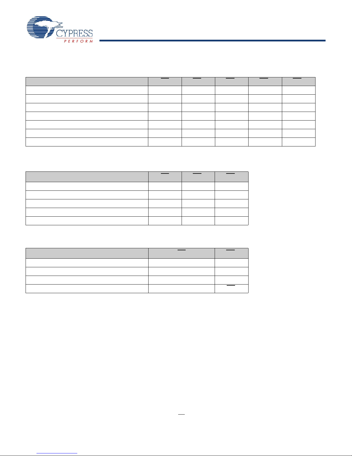
Selection Guide
Description 133 MHz 117 MH z Unit
Maximum Access Time 6.5 8.5 ns
Maximum Operating Current 305 275 mA
Maximum CMOS Standby Current 120 120 mA
Cypress Semiconductor Corporation • 198 Champion Court • San Jose, CA 95134-1709 • 408-943-2600
Document #: 001-15029 Rev. *B Revised March 05, 2008
[+] Feedback
Page 2

CY7C1471BV33
CY7C1473BV33, CY7C1475BV33
Logic Block Diagram – CY7C1471BV33 (2M x 36)
C
MODE
BW
A
BW
B
WE
CE1
CE2
CE3
OE
READ LOGIC
DQs
DQP
A
DQP
B
DQP
C
DQP
D
MEMORY
ARRAY
E
INPUT
REGISTER
BW
C
BW
D
ADDRESS
REGISTER
WRITE REGISTRY
AND DATA COHERENCY
CONTROL LOGIC
BURST
LOGIC
A0'
A1'
D1
D0
Q1
Q0
A0
A1
ADV/LD
CE
ADV/LD
C
CLK
CEN
WRITE
DRIVERS
D
A
T
A
S
T
E
E
R
I
N
G
S
E
N
S
E
A
M
P
S
WRITE ADDRESS
REGISTER
A0, A1, A
O
U
T
P
U
T
B
U
F
F
E
R
S
E
ZZ
SLEEP
CONTROL
C
MODE
BW A
BW B
WE
CE1
CE2
CE3
OE
READ LOGIC
DQs
DQP
A
DQP
B
MEMORY
ARRAY
E
INPUT
REGISTER
ADDRESS
REGISTER
WRITE REGISTRY
AND DATA COHERENCY
CONTROL LOGIC
BURST
LOGIC
A0'
A1'
D1
D0
Q1
Q0
A0
A1
ADV/LD
CE
ADV/LD
C
CLK
C
EN
WRITE
DRIVERS
D
A
T
A
S
T
E
E
R
I
N
G
S
E
N
S
E
A
M
P
S
WRITE ADDRESS
REGISTER
A0, A1, A
O
U
T
P
U
T
B
U
F
F
E
R
S
E
ZZ
SLEEP
CONTROL
Logic Block Diagram – CY7C1473BV33 (4M x 18)
Document #: 001-15029 Rev. *B Page 2 of 32
[+] Feedback
Page 3

CY7C1471BV33
CY7C1473BV33, CY7C1475BV33
Logic Block Diagram – CY7C1475BV33 (1M x 72)
CLK
CEN
A0, A1, A
MODE
C
ADV/LD
BW
BW
BW
BW
BW
BW
BW
BW
WE
CE1
CE2
CE3
ZZ
ADDRESS
REGISTER 0
WRITE ADDRESS
REGISTER 1
a
b
c
d
e
f
g
h
OE
WRITE REGISTRY
AND DATA COHERENCY
CONTROL LOGIC
READ LOGIC
Sleep Control
A1
D1
A0
D0
ADV/LD
C
WRITE ADDRESS
REGISTER 2
BURST
LOGIC
A1'
Q1
A0'
Q0
WRITE
DRIVERS
MEMORY
ARRAY
INPUT
REGISTER 1
O
U
T
P
S
U
E
T
N
S
R
E
E
G
A
I
M
S
P
T
S
E
R
S
E
E
INPUT
REGISTER 0
O
U
T
P
D
U
A
T
T
A
B
U
S
F
T
F
E
E
E
R
R
S
I
N
G
E
DQ s
DQ Pa
DQ Pb
DQ Pc
DQ Pd
DQ Pe
DQ Pf
DQ Pg
DQ Ph
E
Document #: 001-15029 Rev. *B Page 3 of 32
[+] Feedback
Page 4

CY7C1471BV33
CY7C1473BV33, CY7C1475BV33
Pin Configuration
A
A
A
A
A1
A0
NC/288M
NC/144M
V
SS
V
DD
A
A
A
A
A
A
DQP
B
DQ
B
DQ
B
V
DDQ
V
SS
DQ
B
DQ
B
DQ
B
DQ
B
V
SS
V
DDQ
DQ
B
DQ
B
V
SS
NC
V
DD
DQ
A
DQ
A
V
DDQ
V
SS
DQ
A
DQ
A
DQ
A
DQ
A
V
SS
V
DDQ
DQ
A
DQ
A
DQP
A
DQP
C
DQ
C
DQ
C
V
DDQ
V
SS
DQ
C
DQ
C
DQ
C
DQ
C
V
SS
V
DDQ
DQ
C
DQ
C
NC
V
DD
NC
V
SS
DQ
D
DQ
D
V
DDQ
V
SS
DQ
D
DQ
D
DQ
D
DQ
D
V
SS
V
DDQ
DQ
D
DQ
D
DQP
D
A
A
CE
1CE2
BWDBW
C
BWBBWACE3VDDV
SS
CLKWECEN
OE
A
A
1
2
3
4
5
6
7
8
9
10
11
12
13
14
15
16
17
18
19
20
21
22
23
24
25
26
27
28
29
30
3132333435
363738
394041
424344454647484950
80
79
78
77
76
75
74
73
72
71
70
69
68
67
66
65
64
63
62
61
60
59
58
57
56
55
54
53
52
51
100
99989796959493
92919089888786
8584838281
A
A
ADV/LD
ZZ
MODE
A
CY7C1471BV33
BYTE A
BYTE B
BYTE D
BYTE C
A
A
Figure 1. 100-Pin TQFP Pinout
Document #: 001-15029 Rev. *B Page 4 of 32
[+] Feedback
Page 5

CY7C1471BV33
CY7C1473BV33, CY7C1475BV33
Pin Configuration (continued)
A
A
A
A
A1
A0
NC/288M
NC/144M
V
SS
V
DD
A
A
A
A
A
A
A
NC
NC
V
DDQ
V
SS
NC
DQP
A
DQ
A
DQ
A
V
SS
V
DDQ
DQ
A
DQ
A
V
SS
NC
V
DD
DQ
A
DQ
A
V
DDQ
V
SS
DQ
A
DQ
A
NC
NC
V
SS
V
DDQ
NC
NC
NC
NC
NC
NC
V
DDQ
V
SS
NC
NC
DQ
B
DQ
B
V
SS
V
DDQ
DQ
B
DQ
B
NC
V
DD
NC
V
SS
DQ
B
DQ
B
V
DDQ
V
SS
DQ
B
DQ
B
DQP
B
NC
V
SS
V
DDQ
NC
NC
NC
A
A
CE
1CE2
NC
NC
BW
BBWA
CE3VDDV
SS
CLKWECEN
OE
A
A
1
2
3
4
5
6
7
8
9
10
11
12
13
14
15
16
17
18
19
20
21
22
23
24
25
26
27
28
29
30
3132333435363738394041424344454647
484950
80
79
78
77
76
75
74
73
72
71
70
69
68
67
66
65
64
63
62
61
60
59
58
57
56
55
54
53
52
51
100
999897
96
959493929190898887868584838281
A
A
ADV/LD
ZZ
MODE
A
CY7C1473BV33
BYTE A
BYTE B
A
A
Figure 2. 100-Pin TQFP Pinout
Document #: 001-15029 Rev. *B Page 5 of 32
[+] Feedback
Page 6

CY7C1471BV33
CY7C1473BV33, CY7C1475BV33
Pin Configuration (continued)
165-Ball FBGA (15 x 17 x 1.4 mm) Pinout
CY7C1471BV33 (2M x 36)
CY7C1473BV33 (4M x 18)
2345671
A
B
C
D
E
F
G
H
J
K
L
M
N
P
R
TDO
NC/576M
NC/1G
DQP
C
DQ
C
DQP
D
NC
DQ
D
CE
1
BW
B
CE
3
BW
C
CEN
A
CE2
DQ
C
DQ
D
DQ
D
MODE
NC
DQ
C
DQ
C
DQ
D
DQ
D
DQ
D
A
V
DDQ
BW
D
BW
A
CLK
WE
V
SS
V
SS
V
SS
V
SS
V
DDQ
V
SS
V
DD
V
SS
V
SS
V
SS
V
SS
V
SS
V
SS
V
DDQ
V
DDQ
NC
V
DDQ
V
DDQ
V
DDQ
V
DDQ
A
A
V
DD
V
SS
V
DD
V
SS
V
SS
V
DDQ
V
DD
V
SS
V
DD
V
SS
V
DD
V
SS
V
SS
V
SS
V
DD
V
DD
V
SS
V
DD
V
SS
V
SS
NC
TCK
V
SS
TDI
A
A
DQ
C
V
SS
DQ
C
V
SS
DQ
C
DQ
C
NC
V
SS
V
SS
V
SS
V
SS
NC
V
SS
A1
DQ
D
DQ
D
NC/144M
NC
V
DDQ
V
SS
TMS
891011
NC/288M
A
A
ADV/LD
NC
OE
A
NC
V
SS
V
DDQ
NC DQP
B
V
DDQ
V
DD
DQ
B
DQ
B
DQ
B
NC
DQ
B
NC
DQ
A
DQ
A
V
DD
V
DDQ
V
DD
V
DDQ
DQ
B
V
DD
NC
V
DD
DQ
A
V
DD
V
DDQ
DQ
A
V
DDQ
V
DD
V
DD
V
DDQ
V
DD
V
DDQ
DQ
A
V
DDQ
AA
V
SS
A
A
A
DQ
B
DQ
B
DQ
B
ZZ
DQ
A
DQ
A
DQP
A
DQ
A
A
V
DDQ
A
A0
A
V
SS
NC
A
A
2345671
A
B
C
D
E
F
G
H
J
K
L
M
N
P
R
TDO
NC/576M
NC/1G
NC
NC
DQP
B
NC
DQ
B
CE
1
NC
CE
3
BW
B
CEN
A
CE2
NC
DQ
B
DQ
B
MODE
NC
DQ
B
DQ
B
NC
NC
NC
A
V
DDQ
NC BW
A
CLK
WE
V
SS
V
SS
V
SS
V
SS
V
DDQ
V
SS
V
DD
V
SS
V
SS
V
SS
V
SS
V
SS
V
SS
V
DDQ
V
DDQ
NC
V
DDQ
V
DDQ
V
DDQ
V
DDQ
A
A
V
DD
V
SS
V
DD
V
SS
V
SS
V
DDQ
V
DD
V
SS
V
DD
V
SS
V
DD
V
SS
V
SS
V
SS
V
DD
V
DD
V
SS
V
DD
V
SS
V
SS
NC
TCK
V
SS
TDI
A
A
DQ
B
V
SS
NC V
SS
DQ
B
NC
NC
V
SS
V
SS
V
SS
V
SS
NC
V
SS
A1
DQ
B
NC
NC/144M
NC
V
DDQ
V
SS
TMS
891011
NC/288M
A
A
ADV/LD
A
OE
A
NC
V
SS
V
DDQ
NC DQP
A
V
DDQ
V
DD
NC
DQ
A
DQ
A
NC
NC
NC
DQ
A
NC
V
DD
V
DDQ
V
DD
V
DDQ
DQ
A
V
DD
NC
V
DD
NCV
DD
V
DDQ
DQ
A
V
DDQ
V
DD
V
DD
V
DDQ
V
DD
V
DDQ
NC
V
DDQ
AA
V
SS
A
A
A
DQ
A
NC
NC
ZZ
DQ
A
NC
NC
DQ
A
A
V
DDQ
A
A0
A
V
SS
NC
A
A
Document #: 001-15029 Rev. *B Page 6 of 32
[+] Feedback
Page 7

CY7C1471BV33
CY7C1473BV33, CY7C1475BV33
Pin Configuration (continued)
CY7C1475BV33 (1M × 72)
A
B
C
D
E
F
G
H
J
K
L
M
N
P
R
T
U
V
W
123456789 1110
DQg
DQg
DQg
DQg
DQg
DQg
DQg
DQg
DQc
DQc
DQc
DQc
NC
DQPg
DQh
DQh
DQh
DQh
DQd
DQd
DQd
DQd
DQPd
DQPc
DQc
DQc
DQc
DQc
NC
DQh
DQh
DQh
DQh
DQPh
DQd
DQd
DQd
DQd
DQb
DQb
DQb
DQb
DQb
DQb
DQb
DQb
DQf
DQf
DQf
DQf
NC
DQPf
DQa
DQa
DQa
DQa
DQe
DQe
DQe
DQe
DQPa
DQPb
DQf
DQf
DQf
DQf
NC
DQa
DQa
DQa
DQa
DQPe
DQe
DQe
DQe
DQe
AA AA
NC
NC
NC/144M
A A NC/288M
A
AA
AA
A
A1
A0
A
AA
AA
A
NC/576M
NC
NC
NC
NC
NC
BWS
b
BWS
f
BWSeBWS
a
BWScBWS
g
BWS
d
BWS
h
TMS
TDI TDO TCK
NC
NC MODE
NC
CEN
V
SS
NC
CLK
NC
V
SS
V
DD
V
DD
V
DD
V
DD
V
DD
V
DD
V
DD
V
DD
V
DD
V
DD
V
DD
V
DD
V
DD
V
SS
V
SS
V
SS
V
SS
V
SS
V
SS
V
SS
V
SS
NC/1G
V
DD
NC
OE
CE
3
CE
1
CE
2
ADV/LD
WE
V
SS
V
SS
V
SS
V
SS
V
SS
V
SS
V
SS
ZZ
V
SS
V
SS
V
SS
V
SS
NC
V
DDQ
V
SS
V
SS
NC
V
SS
V
SS
V
SS
V
SS
V
SS
V
SS
NC
V
SS
V
DDQ
V
DDQ
V
DDQ
V
DDQ
V
DDQ
NC
V
DDQ
V
DDQ
V
DDQ
V
DDQ
NC
V
DDQ
V
DDQ
V
DDQ
V
DDQ
NC
V
DDQ
V
DDQ
V
DDQ
V
DDQ
V
DDQ
V
DDQ
V
DDQ
V
DDQ
V
DDQ
V
DDQ
209-Ball FBGA (14 x 22 x 1.76 mm) Pinout
Document #: 001-15029 Rev. *B Page 7 of 32
[+] Feedback
Page 8

CY7C1471BV33
CY7C1473BV33, CY7C1475BV33
Pin Definitions
Name IO Description
, A1, A Input-
A
0
BW
BW
BW
BW
, BWB,
A
, BWD,
C
, BWF,
E
, BW
G
H
Synchronous
Synchronous
WE
Synchronous
Input-
Input-
Address Inputs used to select one of the Address Locations. Sampled at the rising edge
of the CLK. A
is fed to the two-bit burst counter.
[1:0]
Byte Write Inputs, Active LOW. Qualified with WE to conduct writes to the SRAM. Sampled
on the rising edge of CLK.
Write Enable Input, Active LOW. Sampled on the rising edge of CLK if CEN is active LOW.
This signal must be asserted LOW to initiate a write sequence.
ADV/LD Input-
Synchronous
CLK Input-
Clock
CE
CE
CE
OE
1
2
3
Input-
Synchronous
Input-
Synchronous
Input-
Synchronous
Input-
Asynchronous
CEN Input-
Synchronous
ZZ Input-
Asynchronous
DQ
s
IO-
Synchronous
Advance/Load Input. Advances the on-chip address counter or loads a new address. When
HIGH (and CEN
address can be loaded into the device for an access. After deselection, drive ADV/LD
is asserted LOW) the internal burst counter is advanced. When LOW, a new
LOW to
load a new address.
Clock Input. Used to capture all synchronous inputs to the device. CLK is qualified with CEN.
CLK is only recognized if CEN
is active LOW.
Chip Enable 1 Input, Active LOW. Sampled on the rising edge of CLK. Used in conjunction
with CE
and CE3 to select or deselect the device.
2
Chip Enable 2 Input, Active HIGH. Sampled on the rising edge of CLK. Used in conjunction
with CE
and CE3 to select or deselect the device.
1
Chip Enable 3 Input, Active LOW. Sampled on the rising edge of CLK. Used in conjunction
with CE
and CE2 to select or deselect the device.
1
Output Enable, Asynchronous Input, Active LOW. Combined with the synchronous logic
block inside the device to control the direction of the IO pins. When LOW, the IO pins are enabled
to behave as outputs. When deasserted HIGH, IO pins are tri-stated, and act as input data pins.
OE
is masked during the data portion of a write sequence, during the first clock when emerging
from a deselected state, and when the device is deselected.
Clock Enable Input, Active LOW. When asserted LOW the clock signal is recognized by the
SRAM. When deasserted HIGH the clock signal is masked. Because deasserting CEN
not deselect the device, CEN
can be used to extend the previous cycle when required.
does
ZZ “Sleep” Input. This active HIGH input places the device in a non-time critical “sleep”
condition with data integrity preserved. During normal operation, this pin must be LOW or left
floating. ZZ pin has an internal pull down.
Bidirectional Data IO Lines. As inputs, they feed into an on-chip data register that is triggered
by the rising edge of CLK. As outputs, they deliver the data contained in the memory location
specified by the addresses presented during the previous
direction of the pins is controlled by OE
When HIGH, DQ
tri-stated during the data portion of a write sequence, during the first clock when emerging from
and DQPX are placed in a tri-state condition.The outputs are automatically
s
. When OE is asserted LOW, the pins behave as outputs.
clock rise of the
read cycle. The
a deselected state, and when the device is deselected, regardless of the state of OE.
DQP
X
IO-
Synchronous
Bidirectional Data Parity IO Lines. Functionally, these signals are identical to DQs. During
write sequences, DQP
MODE Input Strap Pin Mode Input. Selects the Burst Order of the Device. When tied to Gnd selects linear burst
sequence. When tied to VDD or left floating selects interleaved burst sequence.
V
V
V
DD
DDQ
SS
Power Supply Power Supply Inputs to the Core of the Device.
IO Power Supply Power Supply for the IO Circuitry.
Ground Ground for the Device.
Document #: 001-15029 Rev. *B Page 8 of 32
is controlled by BWX correspondingly.
X
[+] Feedback
Page 9

CY7C1471BV33
CY7C1473BV33, CY7C1475BV33
Pin Definitions (continued)
Name IO Description
TDO JTAG serial
output
Synchronous
TDI JTAG serial input
Synchronous
Serial Data-Out to the JT AG Circuit . Delivers data on the negative edge of TCK. If the JTAG
feature is not used, this pin must be left unconnected. This pin is not available on TQFP
packages.
Serial Data-In to the JT AG Circuit. Sampled on the rising edge of TCK. If the JT AG feature is
not used, this pin can be left floating or connected to V
not available on TQFP packages.
through a pull up resistor. This pin is
DD
TMS JTAG serial input
Synchronous
TCK JTAG
-Clock
Serial Data-In to the JT AG Circuit. Sampled on the rising edge of TCK. If the JT AG feature is
not used, this pin can be disconnected or connected to V
packages.
. This pin is not available on TQFP
DD
Clock Input to the JTAG Circuitry. If the JT AG feat ure is not used, this p in must be connected
to V
. This pin is not available on TQFP packages.
SS
NC - No Connects. Not internally connected to the die. 144M, 288M, 576M, and 1G are address
expansion pins and are not internally connected to the die.
Functional Overview
The CY7C1471BV33, CY7C1473BV33, and CY7C1475BV33
are synchronous flow through burst SRAMs designed
specifically to eliminate wait states during write-read transitions.
All synchronous inputs pass through input registers controlled by
the rising edge of the clock. The clock signal is qualified with the
Clock Enable input signal (CEN
is not recognized and all internal states are maintained. All
synchronous operations are qualified with CEN
access delay from the clock rise (t
device).
Accesses may be initiated by asserting all three Chip Enables
(CE
, CE2, CE3) active at the rising edge of the clock. If (CEN)
1
is active LOW and ADV/LD
presented to the device is latched. The access can either be a
read or write operation, depending on the status of the Write
Enable (WE
). Byte Write Select (BWX) can be used to conduct
Byte Write operations.
Write operations are qualified by the Write Enable (WE
writes are simplified with on-chip synchronous self timed write
circuitry.
Three synchronous Chip Enables (CE
asynchronous Output Enable (OE
operations (reads, writes, and deselects) are pipelined. ADV/LD
must be driven LOW after the device is deselected to load a new
address for the next operation.
). If CEN is HIGH, the clock signal
. Maximum
) is 6.5 ns (133 MHz
CDV
is asserted LOW, the address
). All
, CE2, CE3) and an
1
) simplify depth expansion. All
Single Read Accesses
A read access is initiated when these conditions are satisfied at
clock rise:
■ CEN is asserted LOW
■ CE
, CE2, and CE3 are ALL asserted active
1
■ WE is deasserted HIGH
■ ADV/LD is asserted LOW
The address presented to the address inputs is latched into the
Address Register and presented to the memory array and control
logic. The control logic determines that a read access is in
progress and allows the requested data to propagate to the
output buffers. The data is available within 6.5 ns (133 MHz
device) provided OE
read access, the output buffers are controlled by OE
internal control logic. OE
is active LOW. After the first clock of the
and the
must be driven LOW to drive out the
requested data. On the subsequent clock, another operation
(read/write/deselect) can be initiated. When the SRAM is
deselected at clock rise by one of the chip enable signals, output
is tri-stated immediately.
Burst Read Accesses
The CY7C1471BV33, CY7C1473BV33, and CY7C1475BV33
have an on-chip burst counter that enables the user to supply a
single address and conduct up to four reads without reasserting
the address inputs. ADV/LD
must be driven LOW to load a new
address into the SRAM, as described in the Single Read Access
section. The sequence of the burst counter is determined by the
MODE input signal. A LOW input on MODE selects a linear burst
mode, a HIGH selects an interleaved burst sequence. Both burst
counters use A0 and A1 in the burst sequence, and wrap around
when incremented sufficiently. A HIGH input on ADV/LD
increments the internal burst counter regardless of the state of
chip enable inputs or WE
. WE is latched at the beginning of a
burst cycle. Therefore, the type of access (read or write) is
maintained throughout the burst sequence.
Document #: 001-15029 Rev. *B Page 9 of 32
[+] Feedback
Page 10

CY7C1471BV33
CY7C1473BV33, CY7C1475BV33
Single Write Accesses
Write accesses are initiated when the following conditions are
satisfied at clock rise: (1) CEN
and CE
The address presented to the address bus is loaded into the
are all asserted active, and (3) WE is asserted LOW.
3
Address Register. The Write signals are latched into the Control
Logic block. The data lines are automatically tri-stated
regardless of the state of the OE
external logic to present the data on DQs and DQP
On the next clock rise the data presented to DQs and DQP
a subset for Byte Write operations, see section Truth Table for
Read/Write on page 12 for details), input is latched into the
device and the write is complete. Additional accesses
(read/write/deselect) can be initiated on this cycle.
The data written during the write operation is controlled by BW
signals. The CY7C1471BV33, CY7C1473BV33, and
CY7C1475BV33 provide Byte Write capability that is described
in the section Truth Table for Read/Write on page 12. The input
WE
with the selected BWX input selectively writes to only the
desired bytes. Bytes not selected during a Byte Write operation
remain unaltered. A synchronous self timed write mechanism is
provided to simplify the write operations. Byte write capability is
included to greatly simplify read/modify/write sequences, which
can be reduced to simple byte write operations.
Because the CY7C1471BV33, CY7C1473BV33, and
CY7C1475BV33 are common IO devices, do not drive data into
the device when the outputs are active. The Output Enable (OE
can be deasserted HIGH before presenting data to the DQs and
DQPX inputs. Doing so tri-states the output drivers. As a safety
precaution, DQs and DQP
the data portion of a write cycle, regardless of the state of OE
is asserted LOW, (2) CE1, CE2,
input signal. This allows the
.
X
are automatically tri-stated during
X
(or
X
.
Burst Write Accesses
The CY7C1471BV33, CY7C1473BV33, and CY7C1475BV33
have an on-chip burst counter that enables the user to supply a
single address and conduct up to four write operations without
reasserting the address inputs. ADV/LD
load the initial address, as described in section Single Write
Accesses on page 10. When ADV/LD
must be driven LOW to
is driven HIGH on the
subsequent clock rise, the Chip Enables (CE
and WE
Drive the correct BW
write the correct bytes of data.
inputs are ignored and the burst counter is incremented.
inputs in each cycle of the burst write to
X
, CE2, and CE3)
1
Sleep Mode
The ZZ input pin is an asynchronous input. Asserting ZZ places
the SRAM in a power conservation “sleep” mode. Two clock
cycles are required to enter into or exit from this “sleep” mode.
While in this mode, data integrity is guaranteed. Accesses
pending when entering the “sleep” mode are not considered valid
and the completion of the operation is not guaranteed. The
device must be deselected before entering the “sleep” mode.
CE
, CE2, and CE3, must remain inactive for the duration of
1
after the ZZ input returns LOW.
t
ZZREC
X
Interleaved Burst Address Table
(MODE = Floating or VDD)
First
Address
A1: A0
Second
Address
A1: A0
Third
Address
A1: A0
Fourth
Address
A1: A0
00 01 10 11
01 00 11 10
10 11 00 01
11 10 01 00
)
Linear Burst Address Table
(MODE = GND)
First
Address
A1: A0
00 01 10 11
01 10 11 00
10 11 00 01
11 00 01 10
Second
Address
A1: A0
Third
Address
A1: A0
Fourth
Address
A1: A0
ZZ Mode Electrical Characteristics
Parameter Description Test Conditions Min Max Unit
I
DDZZ
t
ZZS
t
ZZREC
t
ZZI
t
RZZI
Document #: 001-15029 Rev. *B Page 10 of 32
Sleep mode standby current ZZ > VDD – 0.2V 120 mA
Device operation to ZZ ZZ > VDD – 0.2V 2t
ZZ recovery time ZZ < 0.2V 2t
ZZ active to sleep current This parameter is sampled 2t
ZZ Inactive to exit sleep current This parameter is sampled 0 ns
CYC
CYC
CYC
ns
ns
ns
[+] Feedback
Page 11

CY7C1471BV33
CY7C1473BV33, CY7C1475BV33
The truth table for CY7C1471BV33, CY7C1473BV33, and CY7C1475BV33 follows.
Notes
1. X = “Don't Care.” H = Logic HIGH, L = Logic LOW. BW
X
= L signifies at least one Byte Write Select is active, BWX = Valid signif ies that the de sired Byte W rite Select s
are asserted, see section Truth Table for Read/Write on page 12 for details.
2. Write is defined by BW
X
, and WE. See section Truth Table for Read/Write on page 12.
3. When a Write cycle is detected, all IOs are tri-stated, even during Byte Writes.
4. The DQs and DQP
X
pins are controlled by the current cycle and the OE signal. OE is asynchronous and is not sampled with the clock.
5. CEN
= H, inserts wait states.
6. Device powers up deselected with the IOs in a tri-state condition, regardless of OE
.
7. OE
is asynchronous and is not sampled with the clock rise. It is masked internally during write cycles. During a read cycle DQs and DQPX = tri-state when OE is
inactive or when the device is deselected, and DQs and DQP
X
= data when OE is active.
[1, 2, 3, 4, 5, 6, 7]
Truth Table
Operation
Deselect Cycle None H X X L L X X X L L->H Tri-State
Deselect Cycle None X X H L L X X X L L->H Tri-State
Deselect Cycle None X L X L L X X X L L->H Tri-State
Continue Deselect Cycle None X X X L H X X X L L->H Tri-State
Read Cycle
(Begin Burst)
Read Cycle
(Continue Burst)
NOP/Dummy Read
(Begin Burst)
Dummy Read
(Continue Burst)
Write Cycle
(Begin Burst)
Write Cycle
(Continue Burst)
NOP/Write Abort
(Begin Burst)
Write Abort
(Continue Burst)
Ignore Clock Edge (Stall) Current X X X L X X X X H L->H Sleep Mode None X X X H X X X X X X Tri-State
Address
Used
CE1CE
ZZ ADV/LD WE BWXOE CEN CLK DQ
CE
2
3
External L H L L L H X L L L->H Data Out (Q)
Next X X X L H X X L L L->H Data Out (Q)
External L H L L L H X H L L->H Tri-State
Next X X X L H X X H L L->H Tri-State
External L H L L L L L X L L->H Data In (D)
Next X X X L H X L X L L->H Data In (D)
None L H L L L L H X L L->H Tri-State
Next X X X L H X H X L L->H Tri-State
Document #: 001-15029 Rev. *B Page 11 of 32
[+] Feedback
Page 12
CY7C1471BV33
CY7C1473BV33, CY7C1475BV33
The read/write truth table for CY7C1471BV33 follows.
Note
8. Table only lists a partial listing of the byte write combinations. Any combination of BW
X
is valid. Appropriate write is based on which byte write is active.
Truth Table for Read/Write
[1, 2, 8]
Function
WE BW
A
BW
B
BW
C
BW
D
Read H X X X X
Write No bytes written LHHHH
Write Byte A – (DQ
Write Byte B – (DQ
Write Byte C – (DQ
Write Byte D – (DQ
and DQPA) LLHHH
A
and DQPB)LHLHH
B
and DQPC)LHHLH
C
and DQPD) LHHHL
D
Write All Bytes L L L L L
The read/write truth table for CY7C1473BV33 follows.
[1, 2, 8]
Truth Table for Read/Write
Function
Read H X X
Write – No Bytes Written L H H
Write Byte a – (DQ
Write Byte b – (DQ
and DQPa)LLH
a
and DQPb)LHL
b
Write Both Bytes L L L
The read/write truth table for CY7C1475BV33 follows.
WE BW
[1, 2, 8]
a
BW
b
Truth Table for Read/Write
Function
Read H X
Write – No Bytes Written L H
Write Byte X − (DQ
and DQP
x
x)
Write All Bytes L All BW
WE BW
x
LL
= L
Document #: 001-15029 Rev. *B Page 12 of 32
[+] Feedback
Page 13

CY7C1471BV33
CY7C1473BV33, CY7C1475BV33
IEEE 1149.1 Serial Boundary Scan (JTAG)
The CY7C1471BV33, CY7C1473BV33, and CY7C1475BV33
incorporate a serial boundary scan test access port (TAP). This
port operates in accordance with IEEE Standard 1149.1-1990
but does not have the set of functions required for full 1149.1
compliance. These functions from the IEEE specification are
excluded because their inclusion places an added delay i n the
critical speed path of the SRAM. Note that the TAP controller
functions in a manner that does not conflict with the operation of
other devices using 1149.1 fully compliant TAPs. The TAP
operates using JEDEC-standard 3.3V or 2.5V IO logic levels.
The CY7C1471BV33, CY7C1473BV33, and CY7C1475BV33
contain a TAP controller, instruction register, boundary scan
register, bypass register, and ID register.
Disabling the JTAG Feature
It is possible to operate the SRAM without using the JTAG
feature. To disable the TAP controller, TCK must be tied LOW
(VSS) to prevent clocking of the device. TDI and TMS are
internally pulled up and may be unconnected. They may
alternately be connected to V
must be left unconnected. During power up, the device comes
up in a reset state, which does not interfere with the operation of
the device.
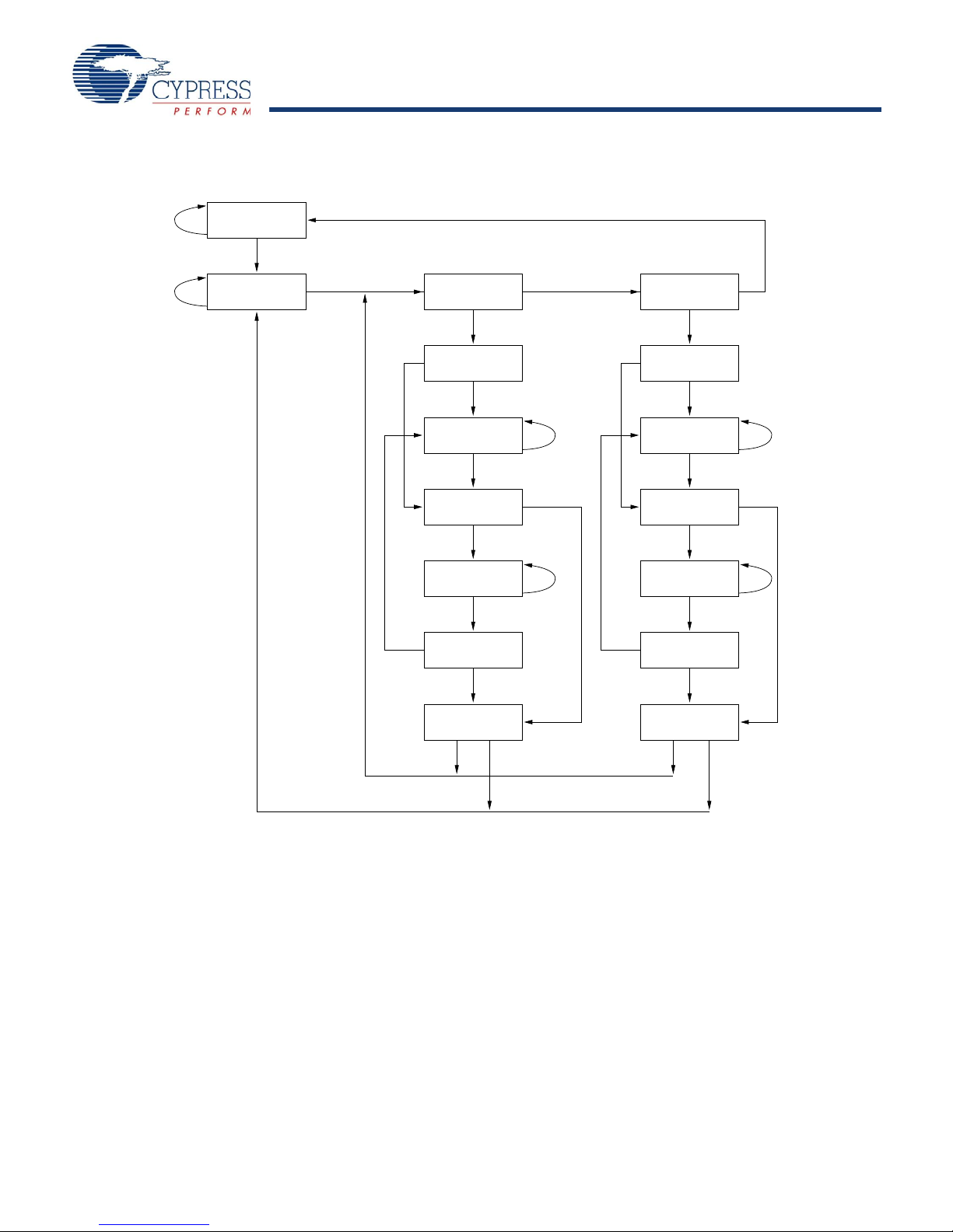
The 0/1 next to each state represents the value of TMS at the
rising edge of TCK.
Test Access Port (TAP)
Test Clock (TCK)
The test clock is used only with the TAP controller. All inputs are
captured on the rising edge of TCK. All outputs are driven from
the falling edge of TCK.
Test MODE SELECT (TMS)
The TMS input gives commands to the TAP controller and is
sampled on the rising edge of TCK. This ball may be left
unconnected if the TAP is not used. The ball is pulled up
internally, resulting in a logic HIGH level.
Test Data-In (TDI)
The TDI ball serially input s information into the registers and can
be connected to the input of any of the registers. The register
between TDI and TDO is chosen by the instruction that is loaded
into the TAP instruction register. For information about loading
the instruction register, see t he TAP Controller State Diagram on
page 15. TDI is internally pulled up and can be unconnected if
the TAP is unused in an application. TDI is connected to the most
significant bit (MSB) of any register. (See the TAP Controller
Block Diagram on page 16.)
Test Data-Out (TDO)
The TDO output ball serially clocks data-out from the registers.
The output is active depending upon the current state of the TAP
state machine. The output changes on the falling edge of TCK.
TDO is connected to the least significant bit (LSB) of any register.
(See TAP Controller State Diagram on page 15.)
through a pull up resistor. TDO
DD
Performing a TAP Reset
A RESET is performed by forcing TMS HIGH (VDD) for five rising
edges of TCK. This RESET does not affect the operation of the
SRAM and may be performed while the SRAM is operating.
During power up, the TAP is reset internally to ensure that TDO
comes up in a High-Z state.
TAP Registers
Registers are connected between the TDI and TDO balls and
enable data to be scanned into and out of the SRAM test circuitry.
Only one register is selected at a time through the instruction
register. Data is serially loaded into the TDI ball on the rising
edge of TCK. Data is output on the TDO ball on the falling edge
of TCK.
nstruction Register
Three-bit instructions can be serially loaded into the instruction
register. This register is loaded when it is placed between the TDI
and TDO balls as shown in the TAP Controller Block Diagram on
page 16. During power up, the instruction register is loaded with
the IDCODE instruction. It is also loaded with the IDCODE
instruction if the controller is placed in a reset state as described
in the previous section.
When the TAP controller is in the Capture-IR state, the two least
significant bits are loaded with a binary ‘01’ pattern to enable fault
isolation of the board-level serial test data path.
Bypass Register
To save time when serially shifting data through registers, it is
sometimes advantageous to skip certain chips. The bypass
register is a single-bit register that can be placed between the
TDI and TDO balls. This allows the shifting of data through the
SRAM with minimal delay. The bypass register is set LOW (V
when the BYPASS instruction is executed.
Boundary Scan Register
The boundary scan register is connected to all the input and
bidirectional balls on the SRAM.
The boundary scan register is loaded with the contents of the
RAM IO ring when the TAP controller is in the Capture-DR state
and is then placed between the TDI and TDO ball s when the
controller is moved to the Shift-DR state. The EXTEST,
SAMPLE/PRELOAD and SAMPLE Z instructions can be used to
capture the contents of the IO ring.
The Boundary Scan Order tables show the order in which the bits
are connected. Each bit corresponds to one of the bumps on the
SRAM package. The MSB of the register is connected to TDI and
the LSB is connected to TDO.
Identification (ID) Register
The ID register is loaded with a vendor-specific, 32-bit code
during the Capture-DR state when the IDCODE command is
loaded in the instruction register. The IDCODE is hardwired into
the SRAM and can be shifted out when the TAP controller is in
the Shift-DR state. The ID register has a vendor code and other
information described in the section Identification Register
Definitions on page 19.
SS
)
Document #: 001-15029 Rev. *B Page 13 of 32
[+] Feedback
Page 14

CY7C1471BV33
CY7C1473BV33, CY7C1475BV33
TAP Instruction Set
Overview
Eight different instructions are possible with the three-bit
instruction register. All combinations are listed in “Identification
Codes” on page 19. Three of these instructions are listed as
RESERVED and must not be used. The other five instructions
are described in detail in this section.
The TAP controller used in this SRAM is not fully compliant to the
1149.1 convention because some of the mandatory 1149.1
instructions are not fully implemented.
The TAP controller cannot be used to load address data or
control signals into the SRAM and cannot preload the IO buffers.
The SRAM does not implement the 1149.1 commands EXTEST
or INTEST or the PRELOAD portion of SAMPLE/PRELOAD;
rather, it performs a capture of the IO ring when these
instructions are executed.
Instructions are loaded into the TAP controller during the Shift-IR
state when the instruction register is placed between TDI and
TDO. During this state, instructions are shifted through the
instruction register through the TDI and TDO balls. To execute
the instruction after it is shifted in, the TAP controller must be
moved into the Update-IR state.
EXTEST
EXTEST is a mandatory 1149.1 instruction which must be
executed whenever the instruction register is loaded wi th all 0s.
EXTEST is not implemented in this SRAM TAP controller, and
therefore this device is not compliant to 1149.1. The TAP
controller does recognize an all-0 instruction.
When an EXTEST instruction is loaded into the instruction
register, the SRAM responds as if a SAMPLE/PRELOAD
instruction has been loaded. There is one difference between the
two instructions. Unlike the SAMPLE/PRELOAD instruction,
EXTEST places the SRAM outputs in a High-Z state.
IDCODE
The IDCODE instruction causes a vendor-specific, 32-bit code
to be loaded into the instruction register. It also places the
instruction register between the TDI and TDO balls and enables
the IDCODE to be shifted out of the device when the TAP
controller enters the Shift-DR state.
The IDCODE instruction is loaded into the instruction register
during power up or whenever the TAP controller is in a test logic
reset state.
SAMPLE/PRELOAD
SAMPLE/PRELOAD is a 1149.1 mandatory instruction. The
PRELOAD portion of this instruction is not implemented, so the
device TAP controller is not fully 1149.1 compliant.
When the SAMPLE/PRELOAD instruction is loaded into the
instruction register and the TAP controller is in the Capture-DR
state, a snapshot of data on the inputs and bidirectional balls is
captured in the boundary scan register.
The user must be aware that the TAP controller clock can only
operate at a frequency up to 20 MHz, while the SRAM clock
operates more than an order of magnitude faster. Because there
is a large difference in the clock frequencies, it is possible that
during the Capture-DR state, an input or output may undergo a
transition. The TAP may then try to capture a signal when in
transition (metastable state). This does not harm the device, but
there is no guarantee as to the value that is captured.
Repeatable results may not be possible.
To guarantee that the boundary scan register captures the
correct value of a signal, the SRAM signal must be stabilized
long enough to meet the TAP controller’s capture setup plus hold
time (t
The SRAM clock input might not be captured correctly if there is
no way in a design to stop (or slow) the clock during a
SAMPLE/PRELOAD instruction. If this is an issue, it is still
possible to capture all other signals and simply ignore the value
of the CLK captured in the boundary scan register.
After the data is captured, it is possible to shift out the data by
putting the TAP into the Shift-DR state. This places the boundary
scan register between the TDI and TDO balls.
Note that because the PRELOAD part of the command is not
implemented, putting the TAP to the Update-DR state when
performing a SAMPLE/PRELOAD instruction has the same
effect as the Pause-DR command.
BYPASS
When the BYPASS instruction is loaded in the instruction register
and the TAP is placed in a Shift-DR state, the bypass register is
placed between the TDI and TDO balls. The advantage of the
BYPASS instruction is that it shortens the boundary scan path
when multiple devices are connected together on a board.
Reserved
These instructions are not implemented but are reserved for
future use. Do not use these instructions.
plus tCH).
CS
SAMPLE Z
The SAMPLE Z instruction causes the boundary scan register to
be connected between the TDI and TDO ba lls when the TAP
controller is in a Shift-DR state. It also places all SRAM outputs
into a High-Z state.
Document #: 001-15029 Rev. *B Page 14 of 32
[+] Feedback
Page 15
CY7C1471BV33
CY7C1473BV33, CY7C1475BV33
TAP Controller State Diagram
TEST-LOGIC
1
0
RESET
0
RUN-TEST/
IDLE
1
SELECT
DR-SCAN
0
1 1
CAPTURE-DR
1
SELECT
IR-SCAN
0
CAPTURE-IR
1
0
SHIFT-DR
1
EXIT1-DR
0 0
PAUSE-DR
1
0 0
EXIT2-DR
1
UPDATE-DR
1 0
0 0
1 1
0
0
SHIFT-IR
1
EXIT1-IR
PAUSE-IR
1
EXIT2-IR
1
UPDATE-IR
1
0
0
Document #: 001-15029 Rev. *B Page 15 of 32
[+] Feedback
Page 16

CY7C1471BV33
CY7C1473BV33, CY7C1475BV33
TAP Controller Block Diagram
Bypass Register
0
Instruction Register
012
Identication Register
012293031 ...
Boundary Scan Register
012..x ...
Selection
Circuitry
TCK
TMS
TAP CONTROLLER
TDI TDO
Selection
Circuitry
Document #: 001-15029 Rev. *B Page 16 of 32
[+] Feedback
Page 17
CY7C1471BV33
CY7C1473BV33, CY7C1475BV33
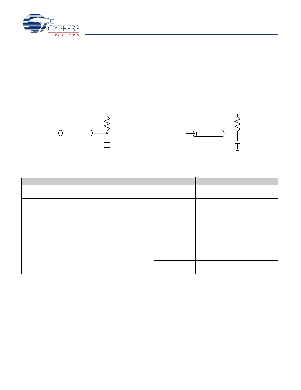
3.3V TAP AC Test Conditions
TDO
1.5V
20pF
Z = 50Ω
O
50Ω
TDO
1.25V
20pF
Z = 50Ω
O
50Ω
Note
9. All voltages refer to V
SS
(GND).
2.5V TAP AC Test Conditions
Input pulse levels.................................................VSS to 3.3V
Input rise and fall times................................................... 1 ns
Input timing reference levels...........................................1.5V
Output reference levels...................................................1.5V
Test load termination supply voltage...............................1.5V
3.3V TAP AC Output Load Equivalent
Input pulse levels................................................ VSS to 2.5V
Input rise and fall time..................................... .. .............. 1 ns
Input timing reference levels.........................................1.25V
Output reference levels.................................................1.25V
Test load termination supply voltage.............................1.25V
2.5V TAP AC Output Load Equivalent
TAP DC Electrical Characteristics and Operating Conditions
(0°C < TA < +70°C; VDD = 3.3V ±0.165V unless otherwise noted)
Parameter Description Test Conditions Min Max Unit
V
V
V
OH1
OH2
OL1
Output HIGH Voltage IOH = –4.0 mA, V
I
= –1.0 mA, V
OH
Output HIGH Voltage IOH = –100 µA V
Output LOW Voltage IOL = 8.0 mA V
IOL = 1.0 mA V
V
OL2
V
IH
V
IL
I
X
Output LOW Voltage IOL = 100 µA V
Input HIGH Voltage V
Input LOW Voltage V
Input Load Current GND < VIN < V
[9]
= 3.3V 2. 4 V
DDQ
= 2.5V 2. 0 V
DDQ
= 3.3V 2.9 V
DDQ
V
= 2.5V 2.1 V
DDQ
= 3.3V 0.4 V
DDQ
= 2.5V 0.4 V
DDQ
= 3.3V 0.2 V
DDQ
V
= 2.5V 0.2 V
DDQ
= 3.3V 2.0 VDD + 0.3 V
DDQ
V
= 2.5V 1.7 VDD + 0.3 V
DDQ
= 3.3V –0.3 0.8 V
DDQ
V
= 2.5V –0.3 0.7 V
DDQ
DDQ
–5 5 µA
Document #: 001-15029 Rev. *B Page 17 of 32
[+] Feedback
Page 18

CY7C1471BV33
CY7C1473BV33, CY7C1475BV33
TAP AC Switching Characteristics
123456
T
Notes
10.t
CS
and tCH refer to the setup and hold time requirement s of l atching d at a fr om t he bound ary scan register.
11.Test conditions are specified using the load in TAP AC Test Conditions. t
R/tF
= 1 ns.
Over the Operating Range
Parameter Description Min Max Unit
Clock
t
TCYC
t
TF
t
TH
t
TL
Output Times
t
TDOV
t
TDOX
Setup Times
t
TMSS
t
TDIS
t
CS
Hold Times
t
TMSH
t
TDIH
t
CH
[10, 11]
TCK Clock Cycle Time 50 ns
TCK Clock Frequency 20 MHz
TCK Clock HIGH time 20 ns
TCK Clock LOW time 20 ns
TCK Clock LOW to TDO Valid 5 ns
TCK Clock LOW to TDO Invalid 0 ns
TMS Setup to TCK Clock Rise 5 ns
TDI Setup to TCK Clock Rise 5 ns
Capture Setup to TCK Rise 5 ns
TMS Hold after TCK Clock Rise 5 ns
TDI Hold after Clock Rise 5 ns
Capture Hold after Clock Rise 5 ns
TAP Timing
Figure 3. TAP Timing
Test Clock
(TCK)
TMSS
t
t
est Mode Select
(TMS)
t
t
TDIS
Test Data-In
(TDI)
Test Data-Out
(TDO)
t
t
TH
TMSH
TDIH
TL
t
CYC
DON’T CARE UNDEFINED
t
TDOX
t
TDOV
Document #: 001-15029 Rev. *B Page 18 of 32
[+] Feedback
Page 19

CY7C1471BV33
CY7C1473BV33, CY7C1475BV33
Identification Register Definitions
Note
12.Bit #24 is “1” in the ID Register Definitions for both 2.5V and 3.3V versions of this device.
Instruction Field
Revision Number (31:29) 000 000 000 D escribes the version number
Device Depth (28:24)
Architecture/Memory Type(23:18) 001001 001001 001001 Defines memory type and architecture
Bus Width/Density(17:12) 100100 010100 110100 Defines width and density
Cypress JEDEC ID Code (11:1) 00000110100 00000110100 00000110100 Enables unique identification of SRAM
ID Register Presence Indicator (0) 1 1 1 Indicates the presence of an ID
[12]
CY7C1471BV33
(2Mx36)
01011 01011 01011 Reserved for internal use
CY7C1473BV33
(4Mx18)
CY7C1475BV33
(1Mx72)
Description
vendor
register
Scan Register Sizes
Register Name Bit Size (x36) Bit Size (x18) Bit Size (x72)
Instruction 3 3 3
Bypass 1 1 1
ID 32 32 32
Boundary Scan Order – 165FBGA 71 52 Boundary Scan Order – 209BGA - - 110
Identification Codes
Instruction Code Description
EXTEST 000 Captures IO ring contents. Places the boundary scan register between TDI
IDCODE 001 Loads the ID register with the vendor ID code and places the register
SAMPLE Z 010 Captures IO ring contents. Places the boundary scan register between TDI
RESERVED 011 Do Not Use: This instruction is reserved for future use.
SAMPLE/PRELOAD 100 Captures IO ring contents. Places the boundary scan register between TDI
RESERVED 101 Do Not Use: This instruction is reserved for future use.
RESERVED 110 Do Not Use: This instruction is reserved for future use.
BYPASS 1 11 Places the bypass register between TDI and TDO. This operation does not
and TDO. Forces all SRAM outputs to High-Z state. This instruction is not
1149.1-compliant.
between TDI and TDO. This operation does not affect SRAM operations.
and TDO. Forces all SRAM output drivers to a High-Z state.
and TDO. Does not affect SRAM operation. This instruction does not
implement 1149.1 preload function and is therefore not 1149.1 compliant.
affect SRAM operations.
Document #: 001-15029 Rev. *B Page 19 of 32
[+] Feedback
Page 20

CY7C1471BV33
CY7C1473BV33, CY7C1475BV33
Boundary Scan Exit Order (2M x 36)
Bit # 165-Ball ID Bit # 165-Ball ID Bit # 165-Ball ID Bit # 165-Ball ID
1C1 21 R3 41J11 61B7
2 D1 22 P2 42 K10 62 B6
3 E1 23 R4 43 J10 63 A6
4D2 24 P6 44H11 64B5
5E2 25 R6 45G11 65A5
6F1 26 R8 46F11 66A4
7G1 27 P3 47E11 67B4
8 F2 28 P4 48 D10 68 B3
9G2 29 P8 49D11 69A3
10 J1 30 P9 50 C11 70 A2
11 K1 31 P10 51 G10 71 B2
12 L1 32 R9 52 F10
13 J2 33 R10 53 E10
14 M1 34 R11 54 A9
15 N1 35 N11 55 B9
16 K2 36 M11 56 A10
17 L2 37 L11 57 B10
18 M2 38 M10 58 A8
19 R1 39 L10 59 B8
20 R2 40 K11 60 A7
Boundary Scan Exit Order (4M x 18)
Bit # 165-Ball ID Bit # 165-Ball ID Bit # 165-Ball ID Bit # 165-Ball ID
1 D2 14 R4 27 L10 40 B10
2E2 15 P6 28K10 41A8
3F2 16 R6 29J10 42B8
4G2 17 R8 30H11 43A7
5J1 18 P3 31G11 44B7
6K1 19 P4 32F11 45B6
7L1 20 P8 33E11 46A6
8M1 21 P9 34D11 47B5
9 N1 22 P10 35 C11 48 A4
10 R1 23 R9 36 A11 49 B3
11 R2 24 R10 37 A9 50 A3
12 R3 25 R11 38 B9 51 A2
13 P2 26 M10 39 A10 52 B2
Document #: 001-15029 Rev. *B Page 20 of 32
[+] Feedback
Page 21

CY7C1471BV33
CY7C1473BV33, CY7C1475BV33
Boundary Scan Exit Order (1M x 72)
Bit # 209-Ball ID Bit # 209-Ball ID Bit # 209-Ball ID Bit # 209-Ball ID
1 A1 29 T1 57 U10 85 B11
2A2 30T2 58T11 86B10
3B1 31U1 59T10 87A11
4B2 32U2 60R11 88A10
5 C1 33 V1 61 R10 89 A7
6C2 34V2 62P11 90A5
7D1 35W1 63P10 91A9
8D2 36W2 64N11 92U8
9 E1 37 T6 65 N10 93 A6
10 E2 38 V3 66 M11 94 D6
11 F1 39 V4 67 M10 95 K6
12 F2 40 U4 68 L11 96 B6
13 G1 41 W5 69 L10 97 K3
14 G2 42 V6 70 P6 98 A8
15 H1 43 W6 71 J11 99 B4
16 H2 44 V5 72 J10 100 B3
17 J1 45 U5 73 H11 101 C3
18 J2 46 U6 74 H10 102 C4
19 L1 47 W7 75 G11 103 C8
20 L2 48 V7 76 G10 104 C9
21 M1 49 U7 77 F11 105 B9
22 M2 50 V8 78 F10 106 B8
23 N1 51 V9 79 E10 107 A4
24 N2 52 W11 80 E11 108 C6
25 P1 53 W10 81 D11 109 B7
26 P2 54 V11 82 D10 110 A3
27 R2 55 V10 83 C11
28 R1 56 U11 84 C10
Document #: 001-15029 Rev. *B Page 21 of 32
[+] Feedback
Page 22

CY7C1471BV33
CY7C1473BV33, CY7C1475BV33
Maximum Ratings
Notes
13.Overshoot: V
IH
(AC) < VDD +1.5V (pulse width less than t
CYC
/2). Undershoot: VIL(AC) > –2V (pulse width less than t
CYC
/2).
14.T
Power-up
: assumes a linear ramp from 0V to VDD(min.) within 200 ms. During this time VIH < VDD and V
DDQ
< VDD.
15.The operation current is calculated with 50% read cycle and 50% write cycle.
Exceeding maximum ratings may impair the useful life of the
device. These user guidelines are not tested.
Storage Temperature .................................–65°C to +150°C
Ambient Temperature with
Power Applied ............................................–55°C to +125°C
Supply Voltage on V
Supply Voltage on V
DC Voltage Applied to Outputs
in Tri-State ...........................................–0.5V to V
Relative to GND........–0.5V to +4.6V
DD
Relative to GND...... –0.5V to +V
DDQ
+ 0.5V
DDQ
DD
DC Input Voltage........................... ........–0.5V to V
Current into Outputs (LOW).........................................20 mA
Static Discharge Voltage........................................... >2001V
(MIL-STD-883, Method 3015)
Latch Up Current.................................................... >200 mA
Operating Range
Range
Commercial 0°C to +70°C 3.3V –5%/+10% 2.5V – 5%
Industrial –40°C to +85°C
Ambient
Temperature
V
DD
+ 0.5V
DD
V
to V
DDQ
DD
Electrical Characteristics
Over the Operating Range
Parameter Description Test Conditions Min Max Unit
V
V
V
V
V
V
I
DD
DDQ
OH
OL
IH
IL
X
Power Supply Voltage 3.135 3.6 V
IO Supply Vol tage For 3.3V IO 3.135 V
Output HIGH Voltage For 3.3V IO, I
Output LOW Voltage For 3.3V IO, I
Input HIGH Voltage
Input LOW Voltage
Input Leakage Current
except ZZ and MODE
Input Current of MODE Input = V
Input Current of ZZ Input = V
I
OZ
I
DD
I
SB1
[15]
Output Leakage Current GND ≤ VI ≤ V
VDD Operating Supply
Current
Automatic CE
Power Down
Current—TTL Inputs
I
SB2
Automatic CE
Power Down
Current—CMOS Inputs
I
SB3
Automatic CE
Power Down
Current—CMOS Inputs
I
SB4
Automatic CE
Power Down
Current—TTL Inputs
[13, 14]
[13]
[13]
DD
For 2.5V IO 2.375 2.625 V
= –4.0 mA 2.4 V
OH
For 2.5V IO, I
For 2.5V IO, I
= –1.0 mA 2.0 V
OH
= 8.0 mA 0.4 V
OL
= 1.0 mA 0.4 V
OL
For 3.3V IO 2.0 VDD + 0.3V V
For 2.5V IO 1.7 VDD + 0.3V V
For 3.3V IO –0.3 0.8 V
For 2.5V IO –0.3 0.7 V
GND ≤ VI ≤ V
Input = V
Input = V
V
= Max., I
DD
f = f
MAX
V
= Max, Device Deselected,
DD
V
≥ VIH or VIN ≤ V
IN
f = f
MAX
V
= Max, Device Deselected,
DD
≤ 0.3V or VIN > VDD – 0.3V,
V
IN
f = 0, inputs static
V
= Max, Device Deselected, or
DD
V
≤ 0.3V or VIN > V
IN
f = f
MAX
V
= Max, Device Deselected,
DD
V
≥ VDD – 0.3V or VIN ≤
IN
f = 0, inputs static
DDQ
SS
DD
SS
DD
Output Disabled –5 5 μA
DD,
= 0 mA,
OUT
= 1/t
CYC
, inputs switching
, inputs switching
IL
DDQ
– 0.3V
,
0.3V
7.5 ns cycle, 133 MHz 305 mA
10 ns cycle, 117 MHz 275 mA
7.5 ns cycle, 133 MHz 200 mA
10 ns cycle, 117 MHz 200 mA
All speeds 120 mA
7.5 ns cycle, 133 MHz 200 mA
10 ns cycle, 117 MHz 200 mA
All Speeds 165 mA
–5 5 μA
–30 μA
5 μA
–5 μA
30 μA
V
Document #: 001-15029 Rev. *B Page 22 of 32
[+] Feedback
Page 23
CY7C1471BV33
CY7C1473BV33, CY7C1475BV33
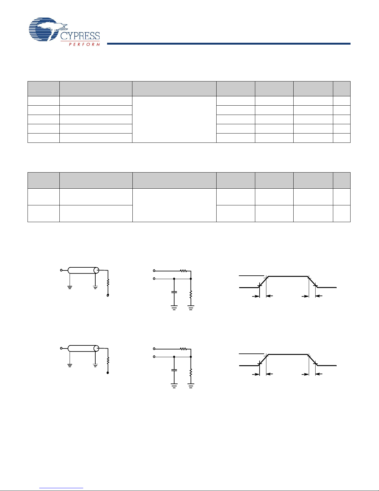
Capacitance
OUTPUT
R = 317Ω
R = 351Ω
5pF
INCLUDING
JIG AND
SCOPE
(a)
(b)
OUTPUT
R
L
= 50Ω
Z
0
= 50Ω
VL= 1.5V
3.3V
ALL INPUT PULSES
V
DDQ
GND
90%
10%
90%
10%
≤ 1 ns
≤ 1 ns
(c)
OUTPUT
R = 1667Ω
R = 1538Ω
5pF
INCLUDING
JIG AND
SCOPE
(a)
(b)
OUTPUT
R
L
= 50Ω
Z
0
= 50Ω
V
L
= 1.25V
2.5V
ALL INPUT PULSES
V
DDQ
GND
90%
10%
90%
10%
≤ 1 ns
≤ 1 ns
(c)
3.3V IO Test Load
2.5V IO Test Load
Tested initially and after any design or process change that may affect these parameters.
Parameter Description Test Conditions
C
ADDRESS
C
DATA
C
CTRL
C
CLK
C
I/O
Address Input Capacitance TA = 25°C, f = 1 MHz,
= 3.3V
V
Data Input Capacitance 5 5 5 pF
Control Input Capacitance 8 8 8 pF
V
DD
DDQ
= 2.5V
Clock Input Capacitance 6 6 6 pF
Input/Output Capacitance 5 5 5 pF
100 TQFP
Package
6 6 6 pF
165 FBGA
Package
209 BGA
Package
Thermal Resistance
Tested initially and after any design or process change that may affect these parameters.
Unit
Parameter Description Test Conditions
Θ
Θ
JA
JC
Thermal Resistance
(Junction to Ambient)
Thermal Resistance
(Junction to Case)
Test conditions follow standard
test methods and procedures for
measuring thermal impedance,
according to EIA/JESD51.
Figure 4. AC Test Loads and Waveforms
100 TQFP
Max
165 FBGA
Max
209 FBGA
Max
24.63 16.3 15.2 °C/W
2.28 2.1 1.7 °C/W
Unit
Document #: 001-15029 Rev. *B Page 23 of 32
[+] Feedback
Page 24

CY7C1471BV33
CY7C1473BV33, CY7C1475BV33
Switching Characteristics
Notes
16.This part has an internal voltage regulator; t
POWER
is the time that the power must be supplied above VDD(minimum) initially , before a read or write operation is initia ted.
17.t
CHZ
, t
CLZ,tOELZ
, and t
OEHZ
are specified with AC test conditions shown in part (b) of AC Test Loads and Waveforms on page 23. Transition is measured ±200 mV
from steady-state voltage.
18.At any supplied voltage and temperature, t
OEHZ
is less than t
OELZ
and t
CHZ
is less than t
CLZ
to eliminate bus contention between SRAMs whe n sharing the same d ata
bus. These specifications do not imply a bus contention conditio n, but refle ct parameters guaranteed over worst case user conditions. Device is designed to achieve
High-Z before Low-Z under the same system conditions.
19.This parameter is sampled and not 100% tested.
Over the Operating Range. Unless otherwise noted in the following table, timing referen ce level is 1.5V when V
1.25V when V
Parameter Description
POWER
[16]
t
= 2.5V. Test conditions shown in (a) of AC Test Loads and Waveforms on page 23 unless otherwise noted.
DDQ
133 MHz 117 MHz
Min Max Min Max
1 1 ms
Clock
t
CYC
t
CH
t
CL
Clock Cycle Time 7.5 10 ns
Clock HIGH 2.5 3.0 ns
Clock LOW 2.5 3.0 ns
Output Times
t
CDV
t
DOH
t
CLZ
t
CHZ
t
OEV
t
OELZ
t
OEHZ
Data Output Valid After CLK Rise 6.5 8.5 ns
Data Output Hold After CLK Rise 2.5 2.5 ns
Clock to Low-Z
Clock to High-Z
[17, 18, 19]
[17, 18, 19]
3.0 3.0 ns
3.8 4.5 ns
OE LOW to Output Valid 3.0 3.8 ns
OE LOW to Output Low-Z
OE HIGH to Output High-Z
[17, 18, 19]
[17, 18, 19]
0 0 ns
3.0 4.0 ns
Setup Times
t
AS
t
ALS
t
WES
t
CENS
t
DS
t
CES
Address Setup Before CLK Rise 1.5 1.5 ns
ADV/LD Setup Before CLK Rise 1.5 1.5 ns
WE, BWX Setup Before CLK Rise 1.5 1.5 ns
CEN Setup Before CLK Rise 1.5 1.5 ns
Data Input Setup Before CLK Rise 1.5 1.5 ns
Chip Enable Setup Before CLK Rise 1.5 1.5 ns
Hold Times
t
AH
t
ALH
t
WEH
t
CENH
t
DH
t
CEH
Address Hold After CLK Rise 0.5 0.5 ns
ADV/LD Hold After CLK Rise 0.5 0.5 ns
WE, BWX Hold After CLK Rise 0.5 0.5 ns
CEN Hold After CLK Rise 0.5 0.5 ns
Data Input Hold After CLK Rise 0.5 0.5 ns
Chip Enable Hold After CLK Rise 0.5 0.5 ns
= 3.3V and is
DDQ
Unit
Document #: 001-15029 Rev. *B Page 24 of 32
[+] Feedback
Page 25

CY7C1471BV33
CY7C1473BV33, CY7C1475BV33
Switching Waveforms
WRITE
D(A1)
123456789
CLK
t
CYC
t
CL
t
CH
10
CE
t
CEH
t
CES
WE
CEN
t
CENH
t
CENS
BWX
ADV/LD
t
AH
t
AS
ADDRESS
A1 A2
A3
A4
A5 A6 A7
t
DH
t
DS
DQ
C
OMMAND
t
CLZ
D(A1) D(A2) Q(A4)Q(A3)
D(A2+1)
t
DOH
t
CHZ
t
CDV
WRITE
D(A2)
BURST
WRITE
D(A2+1)
READ
Q(A3)
READ
Q(A4)
BURST
READ
Q(A4+1)
WRITE
D(A5)
READ
Q(A6)
WRITE
D(A7)
DESELECT
OE
t
OEV
t
OELZ
t
OEHZ
DON’T CARE UNDEFINED
D(A5)
t
DOH
Q(A4+1)
D(A7)Q(A6)
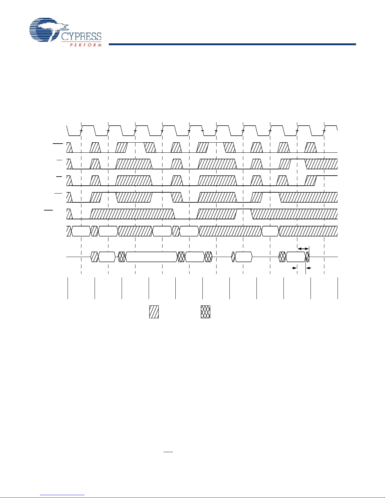
Notes
20.
For this waveform ZZ is tied LOW.
21.When CE
is LOW, CE1 is LOW, CE2 is HIGH, and CE3 is LOW. When CE is HIGH, CE1 is HIGH, CE2 is LOW or CE3 is HIGH.
22.Order of the Burst sequence is determined by the status of the MODE (0 = Linear, 1 = Interleaved). Burst operations are optional.
Figure 5 shows read-write timing waveform.
[20, 21, 22]
Figure 5. Read/Write Timing
Document #: 001-15029 Rev. *B Page 25 of 32
[+] Feedback
Page 26
CY7C1471BV33
CY7C1473BV33, CY7C1475BV33
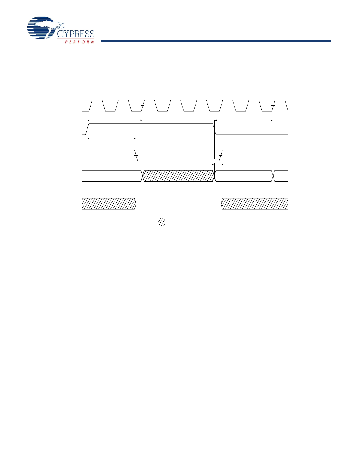
Switching Waveforms (continued)
READ
Q(A3)
456 78910
A3 A4
A5
D(A4)
123
CLK
CE
WE
CEN
BW
[A:D]
ADV/LD
ADDRESS
DQ
C
OMMAND
WRITE
D(A4)
STALLWRITE
D(A1)
READ
Q(A2)
STALL NOP READ
Q(A5)
DESELECT CONTINUE
DESELECT
DON’T CARE UNDEFINED
t
CHZ
A1 A2
Q(A2)D(A1) Q(A3)
t
DOH
Q(A5)
Note
23.The IGNORE CLOCK EDGE or STALL cycle (Clock 3) illustrates CEN
being used to create a pause. A write is not performed during this cycle.
Figure 6 shows NOP, STALL and DESELECT Cycles waveform.
Figure 6. NOP, STALL, and DESELECT Cycles
[20, 21, 23]
Document #: 001-15029 Rev. *B Page 26 of 32
[+] Feedback
Page 27
CY7C1471BV33
CY7C1473BV33, CY7C1475BV33
Switching Waveforms (continued)
A
Notes
24.Device must be deselected when entering ZZ mode. See the The truth table for CY7C1471BV33, CY7C1473 BV3 3, and CY7C14 75BV 33 f oll ows.
[1, 2, 3, 4, 5, 6, 7]
on page 11 for all possible signal conditions to deselect the device.
Figure 7 shows ZZ Mode timing waveform.
CLK
t
ZZ
[24, 25]
Figure 7. ZZ Mode Timing
t
ZZRE C
I
SUPPLY
LL INPUTS
(except ZZ)
Outputs (Q)
ZZ
t
ZZI
I
DDZZ
High-Z
t
RZZI
DESELECT or READ Only
DON’T CARE
Document #: 001-15029 Rev. *B Page 27 of 32
[+] Feedback
Page 28
CY7C1471BV33
CY7C1473BV33, CY7C1475BV33
Ordering Information
Not all of the speed, package, and temperature ranges mentioned here are available. Please contact your local sales
representative or visit www.cypress.com for actual products offered.
Speed
(MHz)
133 CY7C1471BV33-133AXC 51-85050 100-pin Thi n Qua d Flat Pack (14 x 20 x 1.4 mm) Pb-Free Commercial
117 CY7C1471BV33- 117AXC 51-85050 100-pin Thin Quad Fla t Pack (14 x 20 x 1.4 mm) Pb-Free Commercial
Ordering Code
CY7C1473BV33-133AXC
CY7C1471BV33-133BZC 51-85165 165-Ball Fine-Pitch Ball Grid Array (15 x 17 x 1.4 mm)
CY7C1473BV33-133BZC
CY7C1471BV33-133BZXC 51-85165 165-Ball Fine-Pitch Ball Grid Array (15 x 17 x 1.4 mm) Pb-Free
CY7C1473BV33-133BZXC
CY7C1475BV33-133BGC 51-85167 209-Ball Fine-Pitch Ball Grid Array (14 × 22 × 1.76 mm)
CY7C1475BV33-133BGXC 209-Ball Fine-Pitch Ball Grid Array (14 × 22 × 1.76 mm) Pb-Free
CY7C1471BV33-133AXI 51-85050 100-pin Thin Quad Flat Pack (14 x 20 x 1.4 mm) Pb-Free lndustrial
CY7C1473BV33-133AXI
CY7C1471BV33-133BZI 51-85165 165-Bal l Fine-Pitch Ball Grid Array (15 x 17 x 1.4 mm)
CY7C1473BV33-133BZI
CY7C1471BV33-133BZXI 51-85165 165-Ball Fine-Pitch Ball Grid Array (15 x 17 x 1.4 mm) Pb-Free
CY7C1473BV33-133BZXI
CY7C1475BV33-133BGI 51-85167 209-Ball Fine-Pitch Ball Grid Array (14 × 22 × 1.76 mm)
CY7C1475BV33-133BGXI 209-Ball Fine-Pitch Ball Grid Array (14 × 22 × 1.76 mm) Pb-Free
CY7C1473BV33-117AXC
CY7C1471BV33-117BZC 51-85165 165-Ball Fine-Pitch Ball Grid Array (15 x 17 x 1.4 mm)
CY7C1473BV33-117BZC
CY7C1471BV33-117BZXC 51-85165 165-Ball Fine-Pitch Ball Grid Array (15 x 17 x 1.4 mm) Pb-Free
CY7C1473BV33-117BZXC
CY7C1475BV33-117BGC 51-85167 209-Ball Fine-Pitch Ball Grid Array (14 × 22 × 1.76 mm)
CY7C1475BV33-117BGXC 209-Ball Fine-Pitch Ball Grid Array (14 × 22 × 1.76 mm) Pb-Free
CY7C1471BV33-117AXI 51-85050 100-pin Thin Quad Flat Pack (14 x 20 x 1.4 mm) Pb-Free lndustrial
CY7C1473BV33-117AXI
CY7C1471BV33-117BZI 51-85165 165-Ball Fine-Pitch Ball Grid Array (15 x 17 x 1.4 mm)
CY7C1473BV33-117BZI
CY7C1471BV33-117BZXI 51-85165 165-Ball Fine-Pitch Ball Grid Array (15 x 17 x 1.4 mm) Pb-Free
CY7C1473BV33-117BZXI
CY7C1475BV33-117BGI 51-85167 209-Ball Fine-Pitch Ball Grid Array (14 × 22 × 1.76 mm)
CY7C1475BV33-117BGXI 209-Ball Fine-Pitch Ball Grid Array (14 × 22 × 1.76 mm) Pb-Free
Package
Diagram
Part and Package Type
Operating
Range
Document #: 001-15029 Rev. *B Page 28 of 32
[+] Feedback
Page 29

CY7C1471BV33
CY7C1473BV33, CY7C1475BV33
Package Diagrams
NOTE:
1. JEDEC STD REF MS-026
2. BODY LENGTH DIMENSION DOES NOT INCLUDE MOLD PROTRUSION/END FLASH
MOLD PROTRUSION/END FLASH SHALL NOT EXCEED 0.0098 in (0.25 mm) PER SIDE
3. DIMENSIONS IN MILLIMETERS
BODY LENGTH DIMENSIONS ARE MAX PLASTIC BODY SIZE INCLUDING MOLD MISMATCH
0.30±0.08
0.65
20.00±0.10
22.00±0.20
1.40±0.05
12°±1°
1.60 MAX.
0.05 MIN.
0.60±0.15
0° MIN.
0.25
0°-7°
(8X)
STAND-OFF
R 0.08 MIN.
TYP.
0.20 MAX.
0.15 MAX.
0.20 MAX.
R 0.08 MIN.
0.20 MAX.
14.00±0.10
16.00±0.20
0.10
SEE DETAIL
A
DETAIL
A
1
100
30
0513
51
80
81
GAUGE PLANE
1.00 REF.
0.20 MIN.
SEATING PLANE
51-85050 *B
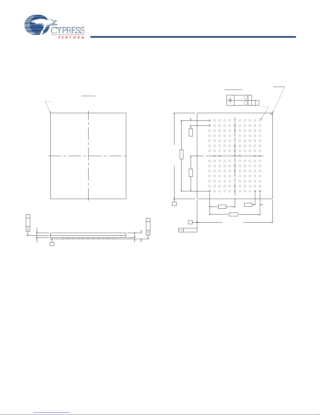
Figure 8. 100-Pin Thin Plastic Quad Fla t pa c k (1 4 x 20 x 1.4 mm)
Document #: 001-15029 Rev. *B Page 29 of 32
[+] Feedback
Page 30
CY7C1471BV33
CY7C1473BV33, CY7C1475BV33
Package Diagrams (continued)
51-85165 *A
Figure 9. 165-Ball FBGA (15 x 17 x 1.4 mm)
1.00
PIN 1 CORNER
1
2345678910
A
B
C
D
E
F
G
H
J
K
L
M
N
P
R
BOTTOM VIEW
TOP VIEW
PIN 1 CORNER
1110986754321
A
B
C
D
E
F
G
H
J
K
L
M
N
P
R
+0.05
0.25 C
0.53±0.05
0.35
-0.10
0.15 C
17.00±0.10
A
1.00
14.00
7.00
B
0.15(4X)
11
Ø0.05 M C
Ø0.25 M C A B
Ø0.45±0.05(165X)
5.00
10.00
15.00±0.10
0.36
SEATING PLANE
C
1.40 MAX.
Document #: 001-15029 Rev. *B Page 30 of 32
[+] Feedback
Page 31
CY7C1471BV33
CY7C1473BV33, CY7C1475BV33
Package Diagrams (continued)
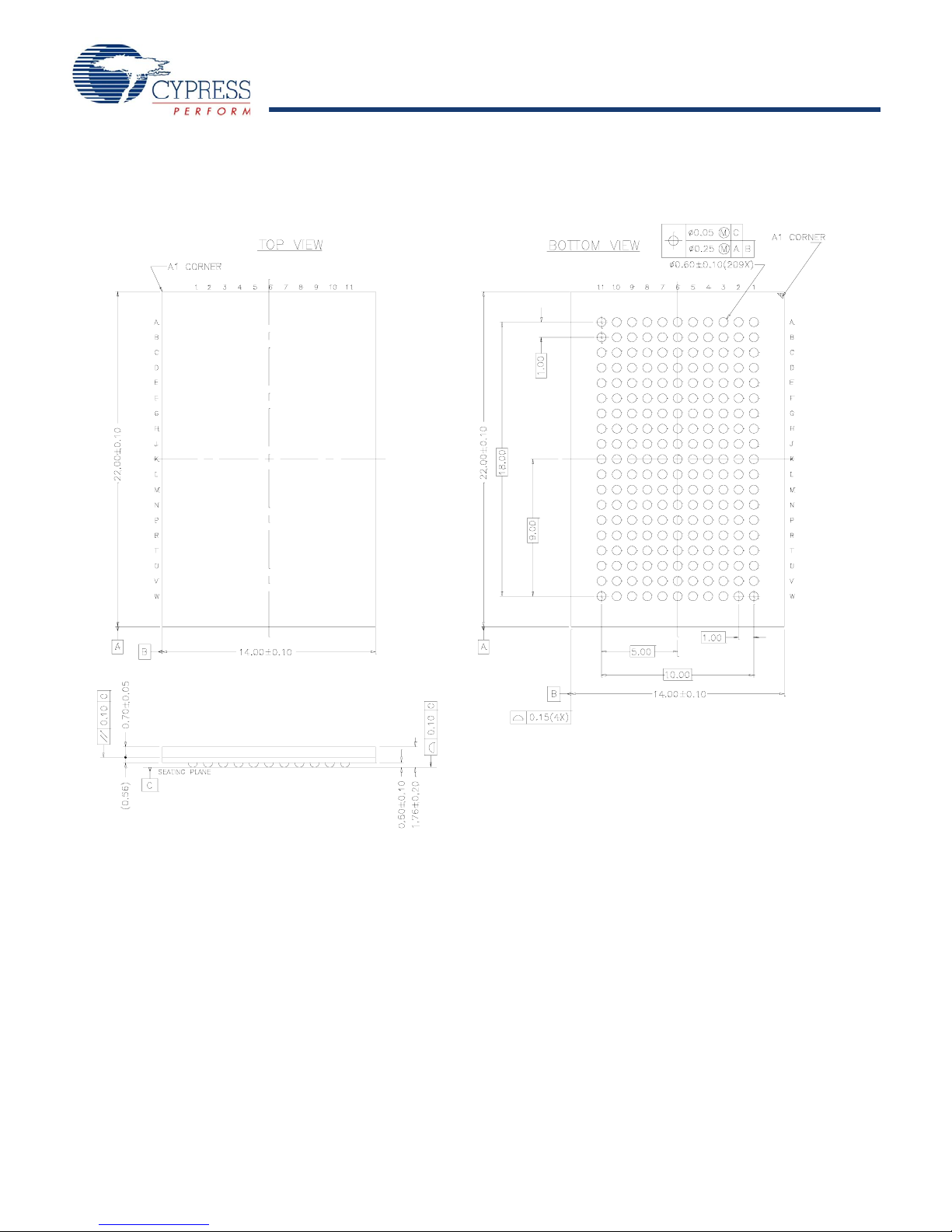
51-85167 **
Figure 10. 209-Ball FBGA (14 x 22 x 1.76 mm)
Document #: 001-15029 Rev. *B Page 31 of 32
[+] Feedback
Page 32

CY7C1471BV33
CY7C1473BV33, CY7C1475BV33
Document History Page
Document Title: CY7C1471BV33/CY7C1473BV33/CY7C1475BV33, 72-Mbit (2M x 36/4M x 18/1M x 72) Flow-Through
SRAM with NoBL™ Architecture
Document Number: 001-15029
REV. ECN NO.
** 1024500 See ECN VKN/KKVTMP New Data Sheet
*A 1274731 See ECN VKN/AESA Corrected typo in the “NOP, STALL and DESELECT Cycles” waveform
*B 2183566 See ECN VKN/PYRS Converted from preliminary to final
Issue
Date
Orig. of Change Description of Change
Added footnote 16 related to IDD
© Cypress Semiconductor Corporation, 2007- 2008. The infor mation cont ain ed herein is subj ect to change wi thout notice. C ypress Semiconductor Corporation assumes no responsibility for the use of
any circuitry other than circuitry embodied in a Cypress product. Nor does it convey or imply any license under patent or other rights. Cypress products are not warranted nor intended to be used fo r
medical, life support, life saving, critica l contr o l or safety applications, unless pursuant to an express written agreemen t w it h Cypr ess. Fu rth er mor e, Cypre ss does not auth or ize i t s pr o ducts for use as
critical components in life-support systems where a malfunction or fa ilure may reasonably be expe cted to result in significa nt injury to the us er . The inclu sion of Cypress p roducts in life -support systems
application implies that the manufacturer assumes all risk of such use and in doing so indemnifies Cypress against all charges.
Any Source Code (software and/or firmware) is owned by Cypress Semiconductor Corporation (Cypress) and is protected by and subject to worldwide patent protection (Un ited States and foreign),
United States copyright laws and international treaty provisions. Cypress hereby gr ant s to l icense e a pers onal, no n-exclu sive , non-tr ansfer able license to copy, use, modify, create d erivative wor ks of,
and compile the Cypress Source Code and derivative works for the sole purpose of creating custom software and or firmware in support of licensee product to be used only in conjunction with a Cy press
integrated circuit as specified in the ap plicable agreem ent. Any reprod uction, modificatio n, translation, co mpilation, or repr esentation of this Source Co de except as speci fied above is pro hibited with out
the express written permission of Cypress.
Disclaimer: CYPRESS MAKES NO WARRANTY OF ANY KIND, EXPRESS OR IMPLIED, WITH REGARD TO THIS MATERIAL, INCLUDING, BUT NOT LIMITED TO, THE IMPLIED WARRANTIES
OF MERCHANTABILITY AND FITNESS FOR A PARTICULAR PURPOSE. Cypress reserves the right to make changes without further notice to the materials described herei n. Cypress d oes not
assume any liability arising out of the applic ation or use o f any pr oduct or circ uit de scribed herein . Cypr ess does n ot author ize its p roducts fo r use as critical compon ents in life-su pport systems whe re
a malfunction or failure may reason ably be expected to result in significant injury to the user. The inclusion of Cypress’ product in a life-support systems application implies that the manufacturer
assumes all risk of such use and in doing so indemnifies Cypress against all charges.
Use may be limited by and subject to the applicable Cypress software license agreement.
Document #: 001-15029 Rev. *B Revised March 05, 2008 Page 32 of 32
NoBL and No Bus Latency are tradem arks of Cypress Semiconductor Corporation. ZBT is a trad emark of Integrated Devi ce T echno logy , Inc. All product and comp any names mentioned in th is document
are the trademarks of their respective holders.
[+] Feedback
 Loading...