

Cypress Semiconductor CY7C130, CY7C130A, CY7C131, CY7C131A, CY7C140 Specification Sheet
...Page 1

CY7C130, CY7C130A
CY7C131, CY7C131A
CY7C140, CY7C141
1K x 8 Dual-Port Static RAM
Features
R/W
L
BUSY
L
CE
L
OE
L
A
9L
A
0L
A
0R
A
9R
R/W
R
CE
R
OE
R
CE
R
OE
R
CE
L
OE
L
R/W
L
R/W
R
I/O
7L
I/O
0L
I/O
7R
I/O
0R
BUSY
R
INT
L
INT
R
ARBITRATION
LOGIC
(7C130/7C131 ONLY)
AND
INTERRUPT LOGIC
CONTROL
I/O
CONTROL
I/O
MEMORY
ARRAY
ADDRESS
DECODER
ADDRESS
DECODER
[2]
[3]
[3]
Logic Block Diagram
Notes
1. CY7C130 and CY7C130A are functionally identical; CY7C131 and CY7C131A are functionally identical.
2. CY7C130/130A/CY7C131/131A (Master): BUSY
is open drain output and requires pull-up resistor .
CY7C140/CY7C141 (Slave): BUSY
is input.
3. Open drain outputs: pull-up resistor required.
■
True dual-ported memory cells, which allow simultaneous
reads of the same memory location
■
1K x 8 organization
■
0.65 micron CMOS for optimum speed and power
■
High speed access: 15 ns
■
Low operating power: ICC = 110 mA (maximum)
■
Fully asynchronous operation
■
Automatic power down
■
Master CY7C130/130A/CY7C131/131A easily expands data
bus width to 16 or more bits using slave CY7C140/CY7C141
■
BUSY output flag on CY7C130/130A/CY7C131/131A; BUSY
input on CY7C140/CY7C141
■
INT flag for port-to-port communication
■
Available in 48-pin DIP (CY7C130/130A/140), 52-pin PLCC,
52-pin TQFP
■
Pb-free packages available
Functional Description
The CY7C130/130A/CY7C131/131A/CY7C140
are high speed CMOS 1K by 8 dual-port static RAMs. Two ports
are provided permitting independent access to any location in
memory. The CY7C130/130A/ CY7C131/131A can be used as
either a standalone 8-bit dual-port static RAM or as a master
dual-port RAM in conjunction with the CY7C140/CY7C141 slave
dual-port device in systems requiring 16-bit or greater word
widths. It is the solution to applications requiring shared or
buffered data, such as cache memory for DSP, bit-slice, or multiprocessor designs.
Each port has independent control pins; chip enable (CE
enable (R/W
on each port, BUSY
), and output enable (OE). Two flags are provided
and INT . BUSY signals that the port is trying
to access the same location currently being accessed by the
other port. INT is an interrupt flag indicating that data is placed
in a unique location (3FF for the left port and 3FE for the right
port). An automatic power down feature is controlled independently on each port by the chip enable (CE
The CY7C130/130A and CY7C140 are available in 48-pin DIP.
The CY7C131/131A and CY7C141 are available in 52-pin
PLCC, 52-pin Pb-free PLCC, 52-pin PQFP, and 52-pin Pb-free
PQFP.
[1]
and CY7C141
) pins.
), write
Cypress Semiconductor Corporation • 198 Champion Court • San Jose,CA 95134-1709 • 408-943-2600
Document #: 38-06002 Rev. *E Revised December 09, 2008
[+] Feedback
Page 2

CY7C130, CY7C130A
CY7C131, CY7C131A
CY7C140, CY7C141
Pin Configurations
13
14
15
16
17
18
19
20
21
22
23 26
27
28
32
31
30
29
33
36
35
34
24 25
GND
1
2
3
4
5
6
7
8
9
10
11
38
39
40
44
43
42
41
45
48
47
46
12 37
R/W
L
CE
L
BUSY
L
INT
L
OE
L
A
0L
A
1L
A
2L
A
3L
A
4L
A
5L
A
6L
A
7L
A
8L
A
9L
I/O
0L
I/O
1L
I/O
2L
I/O
3L
I/O
4L
I/O
5L
I/O
6L
I/O
7L
CE
R
R/W
R
BUSY
R
INT
R
OE
R
A
0R
A
1R
A
2R
A
3R
A
4R
A
5R
A
6R
A
7R
A
8R
A
9R
I/O
7R
I/O
6R
I/O
5R
I/O
4R
I/O
3R
I/O
2R
I/O
1R
I/O
0R
V
CC
7C130
7C140
1
V
CC
OE
R
A
0R
8
9
10
11
12
13
14
15
16
17
18
19
20
46
45
44
43
42
41
40
39
38
37
36
35
34
2122 23 24 25 26 27 28 29 30 31 32 33
7 6 5 4 3 2 52 51 50 49 48 47
A
1R
A
2R
A
3R
A
4R
A
5R
A
6R
A
7R
A
8R
A
9R
NC
I/O
7R
A
1L
A
2L
A
3L
A
4L
A
5L
A
6L
A
7L
A
8L
A
9L
I/O
0L
I/O
1L
I/O
2L
I/O
3L
I/O
I/O
I/O
I/O
I/O
I/O
I/O
I/O
I/O
I/O
I/O
4L5L6L
7L
0R1R2R3R4R5R6R
NC
GND
OE
BUSY
INT
A
NC
R/W
CE
R/W
BUSY
INT
NC
0L
L
L
L
L
L
CE
R
R
R
R
7C131
7C141
46
1
2
3
4
5
6
7
8
9
10
11
12
13
39
38
37
36
35
34
33
32
31
30
29
28
27
1415 16 17 18 19 20 21 22 23 24 25 26
52 5150 49 48 47 45 44 43 42 41 40
V
CC
OE
BUSY
INT
A
NC
R/W
CE
R/W
BUSY
INT
NC
0L
L
L
L
L
L
CE
R
R
R
R
OE
R
A
0R
A
1R
A
2R
A
3R
A
4R
A
5R
A
6R
A
7R
A
8R
A
9R
NC
I/O
7R
A
1L
A
2L
A
3L
A
4L
A
5L
A
6L
A
7L
A
8L
A
9L
I/O
0L
I/O
1L
I/O
2L
I/O
3L
I/O
I/O
I/O
I/O
I/O
I/O
I/O
I/O
I/O
I/O
I/O
4L5L6L
7L
0R1R2R3R4R5R6R
NC
GND
7C131
7C141
Figure 1. Pin Diagram - DIP (Top View)
Figure 2. Pin Diagram - PLCC (Top View) Figure 3. Pin Diagram - PQFP (Top View)
Document #: 38-06002 Rev. *E Page 2 of 19
[+] Feedback
Page 3

CY7C130, CY7C130A
CY7C131, CY7C131A
CY7C140, CY7C141
Pin Definitions
Note
4. 15 and 25 ns version available only in PLCC/PQFP packages.
Left Port Right Port Description
CE
L
R/W
L
OE
L
A
0L–A11/12L
–I/O
I/O
0L
INT
L
BUSY
L
V
CC
15/17L
CE
R
R/W
R
OE
R
A0R–A
11/12R
I/O0R–I/O
INT
R
BUSY
R
15/17R
Chip Enable
Read/Write Enable
Output Enable
Address
Data Bus Input/Output
Interrupt Flag
Busy Flag
Power
GND Ground
Selection Guide
[4]
7C131-25
7C141-25
15 25 30 35 45 55 ns
75 65 65 45 45 35 mA
Parameter
Maximum Access Time
Maximum Operating
Com’l/Ind 190 170 170 120 120 110 mA
Current
Maximum Standby
Com’l/Ind
Current
Shaded areas contain preliminary information.
7C131-15
7C131A-15
7C141-15
7C130A-30
[4]
7C130-30
7C131-30
7C140-30
7C141-30
7C130-35
7C131-35
7C140-35
7C141-35
7C130-45
7C131-45
7C140-45
7C141-45
7C130-55
7C131-55
7C140-55
7C141-55
Unit
Document #: 38-06002 Rev. *E Page 3 of 19
[+] Feedback
Page 4

CY7C130, CY7C130A
CY7C131, CY7C131A
CY7C140, CY7C141
Maximum Ratings
[5]
Exceeding maximum ratings may shorten the useful life of the
device. User guidelines are not tested .
°
Storage Temperature .................................–65°C to +150
C
Ambient Temperature with
Power Applied ............................................–55°C to +125°C
Supply Voltage to Ground Potential
(Pin 48 to Pin 24)............................................–0.5V to +7.0V
DC Voltage Applied to Outputs
in High Z State...................................... ... .......–0.5V to +7.0V
DC Input Voltage................................ ... .........–3.5V to +7.0V
Output Current into Outputs (LOW).............................20 mA
Static Discharge Voltage........................................... >2001V
(per MIL-STD-883, Method 3015)
Latch Up Current.................................................... >200 mA
Operating Range
Range Ambient Temperature V
Commercial 0°C to +70°C 5V ± 10%
Industrial –40°C to +85°C 5V ± 10%
[6]
Military
–55°C to +125°C 5V ± 10%
CC
Electrical Characteristics
Over the Operating Range
[7]
Parameter Description Test Conditions
V
OH
V
OL
V
IH
V
IL
I
IX
I
OZ
I
OS
I
CC
I
SB1
I
SB2
I
SB3
I
SB4
Shaded areas contain preliminary information.
Notes
5. The voltage on any input or I/O pin cannot exceed the power pin during power up.
6. T
A
7. See the last page of this specification for Group A subgroup testing information.
8. BUSY
9. Duration of the short circuit should not exceed 30 seconds.
10.This parameter is guaranteed but not tested.
11. At f = f
Output HIGH Voltage VCC = Min, IOH = –4.0 mA 2.4 2.4 2.4 2.4 V
Output LOW Voltage IOL = 4.0 mA 0.4 0.4 0.4 0.4 V
IOL = 16.0 mA
[8]
Input HIGH Voltage 2.2 2.2 2.2 2.2 V
Input LOW Voltage 0.8 0.8 0.8 0.8 V
Input Leakage Current GND < VI < V
Output Leakage
Current
Output Short
Circuit Current
[9, 10]
VCC Operating
Supply Current
Standby Current
Both Ports, TTL Inputs
Standby Current
One Port,
TTL Inputs
Standby Current
Both Ports,
CMOS Inputs
Standby Current
One Port,
CMOS Inputs
is the “instant on” case temperature
and INT pins only.
, address and data inputs are cycling at the maximum frequency of read cycle of 1/tRC and using AC Test Waveforms input levels of GND to 3V.
MAX
GND < VO < VCC,
Output Disabled
VCC = Max,
V
= GND
OUT
CE = VIL,
Outputs Open, f = f
CEL and CER > VIH,
f = f
MAX
CE
or CER > VIH,
L
Active Port Outputs Open
f = f
MAX
Both Ports CEL and CER >
– 0.2V,
V
CC
V
> VCC – 0.2V
IN
or V
< 0.2V, f = 0
IN
One Port CEL or
> VCC – 0.2V,
CE
R
V
> VCC – 0.2V
IN
or V
< 0.2V,
IN
Active Port Outputs Open, f =
[11]
f
MAX
[11]
[11]
CC
MAX
[11]
[4]
7C130-35,45
7C131-35,45
7C140-35,45
7C141-35,45
7C130-55
7C131-55
7C140-55
7C141-55
Unit
7C131-15
7C131A-15
7C141-15
7C130-30
[4]
7C130A-30
7C131-25,30
7C140-30
7C141-25,30
Min Max Min Max Min Max Min Max
0.5 0.5 0.5 0.5
–5 +5 –5 +5 –5 +5 –5 +5 μA
–5 +5 –5 +5 –5 +5 –5 +5 μA
–350 –350 –350 –350 mA
Com’l 190 170 120 110 mA
Com’l 75 65 45 35 mA
Com’l 135 115 90 75 mA
Com’l
15 15 15 15 mA
Com’l 125 105 85 70 mA
Document #: 38-06002 Rev. *E Page 4 of 19
[+] Feedback
Page 5

CY7C130, CY7C130A
CY7C131, CY7C131A
CY7C140, CY7C141
Capacitance
3.0V
5V
OUTPUT
R1 893Ω
R2
347Ω
30 pF
INCLUDING
JIGAND
SCOPE
GND
90%
90%
10%
≤ 5ns
≤5
ns
5V
OUTPUT
R1 893Ω
R2
347Ω
5pF
INCLUDING
JIGAND
SCOPE
(a)
(b)
OUTPUT 1.40V
Equivalent to:
THÉVENIN EQUIVALENT
5V
281Ω
30
pF
BUSY
OR
INT
BUSY Output Load
(CY7C130/CY7C131 ONLY)
10%
ALL INPUT PULSES
250Ω
[10]
Parameter Description Test Conditions Max Unit
C
IN
C
OUT
Input Capacitance TA = 25°C, f = 1 MHz,
= 5.0V
V
Output Capacitance 10 pF
CC
15 pF
Figure 4. AC Test Loads and Waveforms
Document #: 38-06002 Rev. *E Page 5 of 19
[+] Feedback
Page 6

CY7C130, CY7C130A
CY7C131, CY7C131A
CY7C140, CY7C141
Switching Characteristics
Notes
12.Test conditions assume signal transition times of 5 ns or less , timing ref erence levels of 1.5 V, input pulse levels of 0 to 3.0V an d output loa ding of the specif ied
I
OL/IOH,
and 30 pF load capacitance.
13.AC Test Conditions use V
OH
= 1.6V and VOL = 1.4V.
14.At any given temperature and voltage condition for any given device, t
HZCE
is less than t
LZCE
and t
HZOE
is less than t
LZOE
.
15.t
LZCE
, t
LZWE
, t
HZOE
, t
LZOE
, t
HZCE
and t
HZWE
are tested with CL = 5 pF as in part (b) of AC Test Loads. Transit ion is measured ±500 mV from steady st ate voltage .
16.The internal write time of the memory is defined by the overlap of CS
LOW and R/W LOW. Both signals must be low to initiate a write and either signal can
terminate a write by going high. The data input setup and hold timing should be referenced to the rising edge of the signal that terminates the write.
Over the Operating Range
[7, 12]
Parameter Description
Read Cycle
t
RC
t
AA
t
OHA
t
ACE
t
DOE
t
LZOE
t
HZOE
t
LZCE
t
HZCE
t
PU
t
PD
Write Cycle
t
WC
t
SCE
t
AW
t
HA
t
SA
t
PWE
t
SD
t
HD
t
HZWE
t
LZWE
Shaded areas contain preliminary information.
Read Cycle Time 15 25 30 ns
Address to Data Valid
[13]
Data Hold from Address Change 0 00ns
CE LOW to Data Valid
OE LOW to Data Valid
OE LOW to Low Z
OE HIGH to High Z
CE LOW to Low Z
CE HIGH to High Z
CE LOW to Power Up
[13]
[13]
[10, 14, 15]
[10, 14, 15]
[10, 14, 15]
[10, 14, 15]
[10]
CE HIGH to Power Down
[16]
Write Cycle Time 15 25 30 ns
CE LOW to Write End 12 20 25 ns
Address Setup to Write End 12 20 25 ns
Address Hold from Write End 2 22ns
Address Setup to Write Start 0 00ns
R/W Pulse Width 12 15 25 ns
Data Setup to Write End 10 15 15 ns
Data Hold from Write End 0 00ns
R/W LOW to High Z
R/W HIGH to Low Z
[15]
[15]
[10]
7C131-15
7C131A-15
7C141-15
[4]
7C130-25
[4]
7C131-25
7C140-25
7C141-25
7C130-30
7C130A-30
7C131-30
7C140-30
7C141-30
Unit
Min Max Min Max Min Max
15 25 30 ns
15 25 30 ns
10 15 20 ns
3 33ns
10 15 15 ns
3 55ns
10 15 15 ns
0 00ns
15 25 25 ns
10 15 15 ns
0 00ns
Document #: 38-06002 Rev. *E Page 6 of 19
[+] Feedback
Page 7

CY7C130, CY7C130A
CY7C131, CY7C131A
CY7C140, CY7C141
Switching Characteristics
Notes
17.These parameters are measured from the input signal changing, until the output pin goes to a high-impedance state.
18.CY7C140/CY7C141 only.
19.A write operation on Port A, where Port A has priority, leaves the data on Port B’s outputs undisturbed until one access time after one of the following:
BUSY
on Port B goes HIGH.
Port B’s address is toggled.
CE
for Port B is toggled.
R/W
for Port B is toggled during valid read.
Over the Operating Range
Parameter Description
Busy/Interrupt Timing
t
BLA
t
BHA
t
BLC
t
BHC
t
PS
t
WB
t
WH
t
BDD
t
DDD
t
WDD
[18]
BUSY LOW from Address Match 15 20 20 ns
BUSY HIGH from Address Mismatch
BUSY LOW from CE LOW 15 20 20 ns
BUSY HIGH from CE HIGH
Port Set Up for Priority 5 55ns
R/W LOW af ter BUSY LOW 0 00ns
R/W HIGH after BUSY HI GH 13 20 30 ns
BUSY HIGH to Valid Data 15 25 30 ns
Write Data Valid to Read Data Valid Note 19 Note 19 Note 19 ns
Write Pulse to Dat a Delay Note 19 Note 19 Note 19 ns
Interrupt Timing
t
WINS
t
EINS
t
INS
t
OINR
t
EINR
t
INR
Shaded areas contain preliminary information.
R/W to INTERRUPT Set T ime 15 25 25 ns
CE to INTERRUPT Set Time 15 25 25 ns
Address to INTERRUPT Set Time 15 25 25 ns
OE to INTERRUPT Reset Time
CE to INTERRUPT Reset Time
Address to INTERRUPT Reset Time
[17]
[17]
[17]
[17]
[17]
[7, 12]
(continued)
7C131-15
7C131A-15
7C141-15
[4]
7C130-25
[4]
7C131-25
7C140-25
7C141-25
7C130-30
7C130A-30
7C131-30
7C140-30
7C141-30
Min Max Min Max Min Max
15 20 20 ns
15 20 20 ns
15 25 25 ns
15 25 25 ns
15 25 25 ns
Unit
Document #: 38-06002 Rev. *E Page 7 of 19
[+] Feedback
Page 8

CY7C130, CY7C130A
CY7C131, CY7C131A
CY7C140, CY7C141
Switching Characteristics
Over the Operating Range
[7,12]
Parameter Description
Read Cycle
t
RC
t
AA
t
OHA
t
ACE
t
DOE
t
LZOE
t
HZOE
t
LZCE
t
HZCE
t
PU
t
PD
Write Cycle
t
WC
t
SCE
t
AW
t
HA
t
SA
t
PWE
t
SD
t
HD
t
HZWE
t
LZWE
Read Cycle Time 35 45 55 ns
Address to Data Valid
[13]
Data Hold from Address Change 0 0 0 ns
CE LOW to Data V alid
OE LOW to Data Valid
OE LOW to Low Z
OE HIGH to High Z
CE LOW to Low Z
CE HIGH to High Z
CE LOW to Power Up
[13]
[13]
[10, 14, 15]
[10, 14, 15]
[10, 14, 15]
[10, 14, 15]
[10]
CE HIGH to Power Down
[16]
Write Cycle Time 35 45 55 ns
CE LOW to Write End 30 35 40 ns
Address Setup to Write End 30 35 40 ns
Address Hold from Write End 2 2 2 ns
Address Setup to Write Start 0 0 0 ns
R/W Pulse Width 25 30 30 ns
Data Setup to Write End 15 20 20 ns
Data Hold from Write End 0 0 0 ns
R/W LOW to High Z
R/W HIGH to Low Z
[15]
[15]
Busy/Interrupt Timing
t
BLA
t
BHA
t
BLC
t
BHC
t
PS
t
WB
t
WH
t
BDD
t
DDD
t
WDD
[18]
BUSY LOW from Address Match 20 25 30 ns
BUSY HIGH from Address Mismatch
BUSY LOW from CE LOW 20 25 30 ns
BUSY HIGH from CE HIGH
Port Set Up for Priority 5 5 5 ns
R/W LOW after BUSY LOW 0 0 0 ns
R/W HIGH after BUSY HIGH 30 35 35 ns
BUSY HIGH to Valid Data 35 45 45 ns
Write Data Valid to Read Data Valid Note 19 Note 19 Note 19 ns
Write Pulse to Data Delay Note 19 Note 19 Note 19 ns
Interrupt Timing
t
WINS
t
EINS
t
INS
t
OINR
t
EINR
t
INR
R/W to INTERRUP T S et Time 25 35 45 ns
CE to INTERRUPT Set Time 25 35 45 ns
Address to INTERRUPT S e t Ti m e 25 35 45 ns
OE to INTERRUPT Reset Time
CE to INTERRUPT Reset Time
Address to INTERRUPT Reset T ime
[10]
[17]
[17]
[17]
[17]
[17]
7C130-35
7C131-35
7C140-35
7C141-35
7C130-45
7C131-45
7C140-45
7C141-45
7C130-55
7C131-55
7C140-55
7C141-55
Unit
Min Max Min Max Min Max
35 45 55 ns
35 45 55 ns
20 25 25 ns
333ns
20 20 25 ns
555ns
20 20 25 ns
000ns
35 35 35 ns
20 20 25 ns
000ns
20 25 30 ns
20 25 30 ns
25 35 45 ns
25 35 45 ns
25 35 45 ns
Document #: 38-06002 Rev. *E Page 8 of 19
[+] Feedback
Page 9

CY7C130, CY7C130A
CY7C131, CY7C131A
CY7C140, CY7C141
Switching Waveforms
t
RC
t
AA
t
OHA
DATA VALIDPREVIOUS DATA VALID
DATA OUT
ADDRESS
Either Port Address Access
t
ACE
t
LZOE
t
DOE
t
HZOE
t
HZCE
DATA VALID
DATA OUT
CE
OE
t
LZCE
t
PU
I
CC
I
SB
t
PD
Either Port CE/OE Access
t
BHA
t
BDD
VALID
t
DDD
t
WDD
ADDRESS MATCH
ADDRESS MATCH
R/W
R
ADDRESS
R
D
INR
ADDRESS
L
BUSY
L
DOUT
L
t
PS
t
BLA
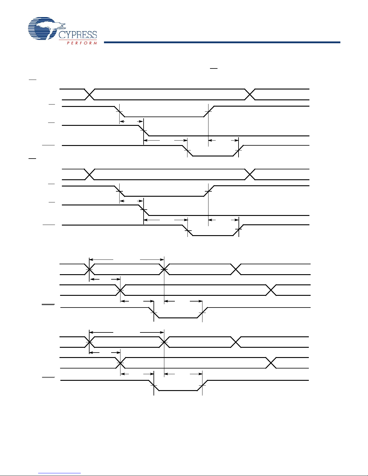
Read with BUSY, Master: CY7C130 and CY7C131
t
RC
t
PWE
VALID
t
HD
Figure 5. Read Cycle No. 1
[20, 21]
Figure 6. Read Cycle No. 2
Figure 7. Read Cycle No. 3
[20, 22]
[21]
= VIL and OE = VIL.
transition LOW.
Notes
is HIGH for read cycle.
20.R/W
21.Device is continuously selected, CE
22.Address valid prior to or coincident with CE
Document #: 38-06002 Rev. *E Page 9 of 19
[+] Feedback
Page 10

CY7C130, CY7C130A
CY7C131, CY7C131A
CY7C140, CY7C141
Switching Waveforms
t
AW
t
WC
DATA VALID
HIGH IMPEDANCE
t
SCE
t
SA
t
PWE
t
HD
t
SD
t
HA
CE
R/W
ADDRESS
t
HZOE
OE
D
OUT
DATA
IN
Either Port
t
AW
t
WC
t
SCE
t
SA
t
PWE
t
HD
t
SD
t
HZWE
t
HA
HIGH IMPEDANCE
DATAVALID
t
LZWE
ADDRESS
CE
R/W
DATA
OUT
DATA
IN
Notes
23.If OE
is LOW during a R/W controlled write cycle, the write pulse width must be the larger of t
PWE
or t
HZWE
+ tSD to allow the data I/O pins to enter high impedance
and for data to be placed on the bus for the required t
SD
.
24.If the CE
LOW transition occurs simultaneously with or after the R/W LOW transition, the outputs remain in the high impedance state.
Figure 8. Write Cycle No. 1 (OE Three-States Data I/Os—Either Port
(continued)
[16, 23]
Figure 9. Write Cycle No. 2 (R/W Three-States Data I/Os—Either Port)
Document #: 38-06002 Rev. *E Page 10 of 19
[17, 24]
[+] Feedback
Page 11
CY7C130, CY7C130A
CY7C131, CY7C131A
CY7C140, CY7C141
Switching Waveforms
ADDRESS MATCH
t
PS
CEL Valid First:
t
BLC
t
BHC
ADDRESS MATCH
t
PS
t
BLC
t
BHC
ADDRESS
L,R
BUSY
R
CE
L
CE
R
BUSY
L
CE
R
CE
L
ADDRESS
L,R
CER Valid First:
Left Address Valid First:
ADDRESS MATCH
t
PS
ADDRESS
L
BUSY
R
ADDRESS MISMATCH
t
RC
or t
WC
t
BLA
t
BHA
ADDRESS
R
ADDRESS MATCH ADDRESS MISMATCH
t
PS
ADDRESS
L
BUSY
L
tRCor t
WC
t
BLA
t
BHA
ADDRESS
R
Right Address Valid First:
(continued)
Figure 10. Busy Timing Diagram No. 1 (CE Arbitration)
Figure 11. Busy Timing Diagram No. 2 (Address Arbitration)
Document #: 38-06002 Rev. *E Page 11 of 19
[+] Feedback
Page 12

CY7C130, CY7C130A
CY7C131, CY7C131A
CY7C140, CY7C141
Switching Waveforms
t
PWE
t
WB
t
WH
Write with BUSY (Slave:CY7C140/CY7C141)
BUSY
R/W
CE
(continued)
Figure 12. Busy Timing Diagram No. 3
Document #: 38-06002 Rev. *E Page 12 of 19
[+] Feedback
Page 13

CY7C130, CY7C130A
CY7C131, CY7C131A
CY7C140, CY7C141
Switching Waveforms
WRITE 3FF
t
INS
t
WC
t
EINS
Right Side Clears INT
R
t
HA
t
SA
t
WINS
READ 3FF
t
RC
t
EINR
t
HA
t
INT
t
OINR
WRITE 3FE
t
INS
t
WC
t
EINS
t
HA
t
SA
t
WINS
Right Side Sets INT
L
Left Side Sets INT
R
Left Side Clears INT
L
READ 3FE
t
EINR
t
HA
t
INR
t
OINR
t
RC
ADDR
R
CE
L
R/W
L
INT
L
OE
L
ADDR
R
R/W
R
CE
R
INT
L
ADDR
R
CE
R
R/W
R
INT
R
OE
R
ADDR
L
R/W
L
CE
L
INT
R
(continued)
Figure 13. Interrupt Timing Diagrams
Document #: 38-06002 Rev. *E Page 13 of 19
[+] Feedback
Page 14
CY7C130, CY7C130A
CY7C131, CY7C131A
CY7C140, CY7C141
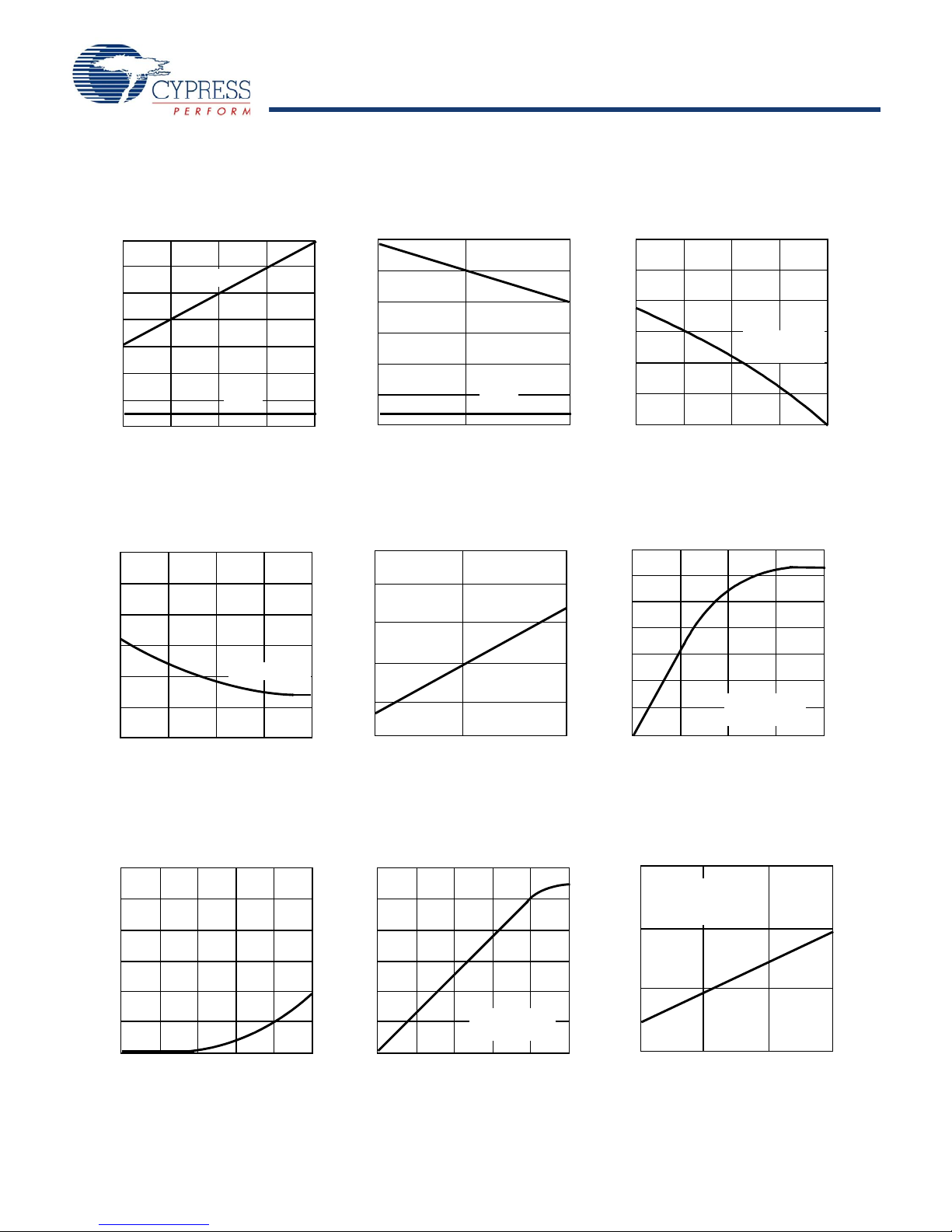
Typical DC and AC Characteristics
1.4
1.0
0.4
4.0 4.5 5.0 5.5 6.0
–55 25 125
1.2
1.0
120
100
80
60
40
20
0 1.0 2.0 3.0 4.0
OUTPUT SOURCE CURRENT (mA)
SUPPLYVOLTAGE (V)
NORMALIZED SUPPLY CURRENT
vs. SUPPLY VOLTAGE
NORMALIZED SUPPLY CURRENT
vs. AMBIENT TEMPERATURE
AMBIENT TEMPERATURE(°C)
OUTPUT VOLTAGE (V)
OUTPUT SOURCE CURRENT
vs. OUTPUT VOLTAGE
0.0
0.8
0.8
0.6
0.6
NORMALIZED I
CC
, I
SB
V
CC
= 5.0V
V
IN
= 5.0V
V
CC
= 5.0V
T
A
= 25°C
0
I
CC
1.6
1.4
1.2
1.0
0.8
–55 125
NORMALIZED t
AA
NORMALIZED ACCESS TIME
vs. AMBIENT TEMPERATURE
AMBIENT TEMPERATURE(°C)
1.4
1.3
1.2
1.0
0.9
4.0 4.5 5.0 5.5 6.0
NORMALIZED t
AA
SUPPLY VOLTAGE (V)
NORMALIZED ACCESS TIME
vs. SUPPLY VOLTAGE
120
140
100
60
40
20
0.0 1.0 2.0 3.0 4.0
OUTPUT SINK CURRENT (mA)
0
80
OUTPUT VOLTAGE (V)
OUTPUT SINK CURRENT
vs. OUTPUT VOLTAGE
0.6
0.8
1.25
1.0
0.75
10 40
NORMALIZED I
CC
0.50
NORMALIZED I
CC
vs. CYCLE TIME
CYCLE FREQUENCY (MHz)
3.0
2.5
2.0
1.5
0.5
0 1.0 2.0 3.0 5.0
NORMALIZED t
PC
25.0
30.0
20.0
10.0
5.0
0 200 400 600 800
DELTA t
AA
(ns)
0
15.0
0.0
SUPPLY VOLTAGE (V)
TYPICAL POWER-ON CURRENT
vs. SUPPLY VOLTAGE
CAPACITANCE (pF)
TYPICAL ACCESS TIME CHANGE
vs. OUTPUT LOADING
4.0
1000
1.0
20 30
0.2
0.6
1.2
I
SB3
0.2
0.4
25
1.1
V
CC
= 4.5V
V
IN
= 0.5V
NORMALIZED I
CC
, I
SB
I
CC
I
SB3
TA = 25°C
V
CC
= 5.0V
V
CC
= 5.0V
T
A
= 25°C
T
A
= 25°C
V
CC
= 4.5V
V
CC
= 4.5V
T
A
= 25°C
Document #: 38-06002 Rev. *E Page 14 of 19
[+] Feedback
Page 15

CY7C130, CY7C130A
CY7C131, CY7C131A
CY7C140, CY7C141
Ordering Information
Speed
(ns)
30 CY7C130-30PC P25 48-Pin (600 Mil) Molded DIP Commercial
35 CY7C130-35PC P25 48-Pin (600 Mil) Molded DIP Commercial
45 CY7C130-45PC P25 48-Pin (600 Mil) Molded DIP Commercial
55 CY7C130-55PC P25 48-Pin (600 Mil) Molded DIP Commercial
15 CY7C131-15JC J69 52-Pin Plastic Leaded Chip Carrier Commercial
25 CY7C131-25JC J69 52-Pin Plastic Leaded Chip Carrier Commercial
30 CY7C131-30JC J69 52-Pin Plastic Leaded Chip Carrier Commercial
35 CY7C131-35JC J69 52-Pin Plastic Leaded Chip Carrier Commercial
45 CY7C131-45JC J69 52-Pin Plastic Leaded Chip Carrier Commercial
55 CY7C131-55JC J69 52-Pin Plastic Leaded Chip Carrier Commercial
30 CY7C140-30PC P25 48-Pin (600 Mil) Molded DIP Commercial
Ordering Code
CY7C130A-30PI P25 48-Pin Pb-Free (600 Mil) Molded DIP Industrial
CY7C130-35PI P25 48-Pin (600 Mil) Molded DIP Industrial
CY7C130-45PI P25 48-Pin (600 Mil) Molded DIP Industrial
CY7C130-55PI P25 48-Pin (600 Mil) Molded DIP Industrial
CY7C131-15JXC J69 52-Pin Pb-Free Plastic Leaded Chip Carrier
CY7C131-15NC N52 52-Pin Plastic Quad Flatpack
CY7C131-15JI J69 52-Pin Plastic Leaded Chip Carrier Industrial
CY7C131A-15JXI J69 52-Pin Pb-Free Plastic Leaded Chip Carrier
CY7C131-15NXI N52 52-Pin Pb-Free Plastic Quad Flatpack
CY7C131-25JXC J69 52-Pin Pb-Free Plastic Leaded Chip Carrier
CY7C131-25NC N52 52-Pin Plastic Quad Flatpack
CY7C131-25NXC N52 52-Pin Pb-Free Plastic Quad Flatpack
CY7C131-25JI J69 52-Pin Plastic Leaded Chip Carrier Industrial
CY7C131-25NI N52 52-Pin Plastic Quad Flatpack
CY7C131-30NC N52 52-Pin Plastic Quad Flatpack
CY7C131-30JI J69 52-Pin Plastic Leaded Chip Carrier Industrial
CY7C131-35NC N52 52-Pin Plastic Quad Flatpack
CY7C131-35JI J69 52-Pin Plastic Leaded Chip Carrier Industrial
CY7C131-35NI N52 52-Pin Plastic Quad Flatpack
CY7C131-45NC N52 52-Pin Plastic Quad Flatpack
CY7C131-45JI J69 52-Pin Plastic Leaded Chip Carrier Industrial
CY7C131-45NI N52 52-Pin Plastic Quad Flatpack
CY7C131-55JXC J69 52-Pin Pb-Free Plastic Leaded Chip Carrier
CY7C131-55NC N52 52-Pin Plastic Quad Flatpack
CY7C131-55NXC N52 52-Pin Pb-Free Plastic Quad Flatpack
CY7C131-55JI J69 52-Pin Plastic Leaded Chip Carrier Industrial
CY7C131-55JXI J69 52-Pin Pb-Free Plastic Leaded Chip Carrier
CY7C131-55NI N52 52-Pin Plastic Quad Flatpack
CY7C131-55NXI N52 52-Pin Pb-Free Plastic Quad Flatpack
CY7C140-30PI P25 48-Pin (600 Mil) Molded DIP Industrial
Package
Name
Package Type
Operating
Range
Document #: 38-06002 Rev. *E Page 15 of 19
[+] Feedback
Page 16
CY7C130, CY7C130A
CY7C131, CY7C131A
CY7C140, CY7C141
Ordering Information
Speed
(ns)
35 CY7C140-35PC P25 48-Pin (600 Mil) Molded DIP Commercial
45 CY7C140-45PC P25 48-Pin (600 Mil) Molded DIP Commercial
55 CY7C140-55PC P25 48-Pin (600 Mil) Molded DIP Commercial
15 CY7C141-15JC J69 52-Pin Plastic Leaded Chip Carrier Commercial
25
30 CY7C141-30JC J69 52-Pin Plastic Leaded Chip Carrier Commercial
35 CY7C141-35JC J69 52-Pin Plastic Leaded Chip Carrier Commercial
45 CY7C141-45JC J69 52-Pin Plastic Leaded Chip Carrier Commercial
55 CY7C141-55JC J69 52-Pin Plastic Leaded Chip Carrier Commercial
Ordering Code
CY7C140-35PI P25 48-Pin (600 Mil) Molded DIP Industrial
CY7C140-45PI P25 48-Pin (600 Mil) Molded DIP Industrial
CY7C140-55PI P25 48-Pin (600 Mil) Molded DIP Industrial
CY7C141-15NC N52 52-Pin Plastic Quad Flatpack
CY7C141-25JC J69 52-Pin Plastic Leaded Chip Carrier Commercial
CY7C141-25JXC J69 52-Pin Pb-Free Plastic Leaded Chip Carrier
CY7C141-25NC N52 52-Pin Plastic Quad Flatpack
CY7C141-25JI J69 52-Pin Plastic Leaded Chip Carrier Industrial
CY7C141-25NI N52 52-Pin Plastic Quad Flatpack
CY7C141-30NC N52 52-Pin Plastic Quad Flatpack
CY7C141-30JI J69 52-Pin Plastic Leaded Chip Carrier Industrial
CY7C141-35NC N52 52-Pin Plastic Quad Flatpack
CY7C141-35JI J69 52-Pin Plastic Leaded Chip Carrier Industrial
CY7C141-35NI N52 52-Pin Plastic Quad Flatpack
CY7C141-45NC N52 52-Pin Plastic Quad Flatpack
CY7C141-45JI J69 52-Pin Plastic Leaded Chip Carrier Industrial
CY7C141-45NI N52 52-Pin Plastic Quad Flatpack
CY7C141-55NC N52 52-Pin Plastic Quad Flatpack
CY7C141-55JI J69 52-Pin Plastic Leaded Chip Carrier Industrial
CY7C141-55NI N52 52-Pin Plastic Quad Flatpack
(continued)
Package
Name
Package Type
Operating
Range
Document #: 38-06002 Rev. *E Page 16 of 19
[+] Feedback
Page 17
CY7C130, CY7C130A
CY7C131, CY7C131A
CY7C140, CY7C141
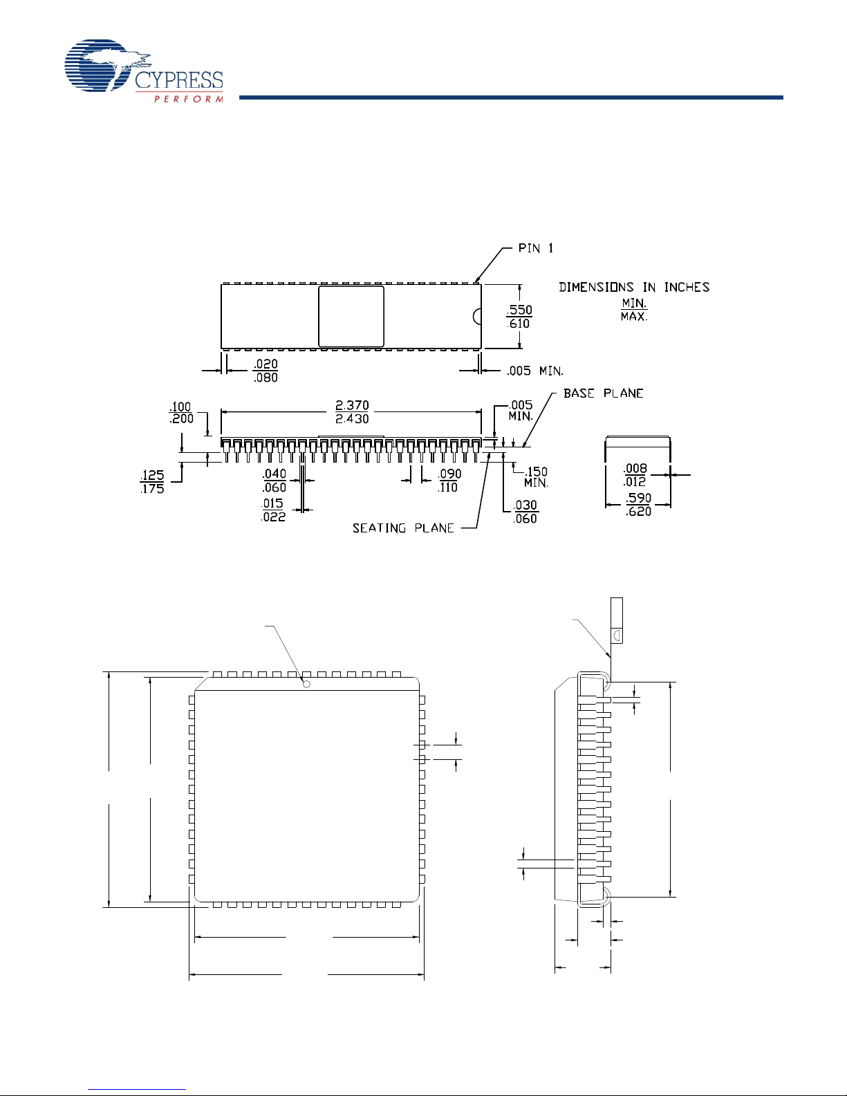
Package Diagrams
MIL-STD-1835 D-14 Config. C
51-80044 **
DIMENSIONS IN INCHES
MIN.
MAX.
0.045
0.055
0.020 MIN.
0.090
0.165
0.023
0.033
0.013
0.785
0.795
0.750
0.756
0.756
0.750
0.795
0.785
0.130
0.200
0.021
0.690
0.730
477
21 33
34
46
20
8
0.004
SEATING PLANE
1
PIN #1 ID
51-85004-*A
Figure 14. 48-Pin (600 Mil) Sidebraze DIP D26
Figure 15. 52-Pin Pb-Free Plastic Leaded Chip Carrier J69
Document #: 38-06002 Rev. *E Page 17 of 19
[+] Feedback
Page 18

CY7C130, CY7C130A
CY7C131, CY7C131A
CY7C140, CY7C141
Package Diagrams
51-85020-*B
51-85042-**
(continued)
Figure 16. 48-Pin (600 Mil) Molded DIP P25
Figure 17. 52-Pin Pb-Free Plastic Quad Flatpack N52
Document #: 38-06002 Rev. *E Page 18 of 19
[+] Feedback
Page 19
CY7C130, CY7C130A
CY7C131, CY7C131A
CY7C140, CY7C141
Document History Page
Document Title: CY7C130/CY7C130A/CY7C131/CY7C131A/CY7C140/CY7C141 1K x 8 Dual-Port Static RAM
Document Number: 38-06002
Rev. ECN No.
Orig. of
Change
Submission
Date
Description of Change
** 110169 SZV 09/29/01 Change from Spec number: 38-00027 to 38-06002
*A 122255 RBI 12/26/02 Power up requirements added to Maximum Ratings Information
*B 23 6751 YDT See ECN Removed cross information from features section
*C 325936 RUY See ECN Added pin definitions table, 52-pin PQFP package diagram and Pb-free
information
*D 393153 YIM See ECN Added CY7C131-15JI to ordering information
Added Pb-Free parts to ordering information:
CY7C131-15JXI
*E 2623540 VKN/PYRS 12/17/08 Added CY7C1 30A and CY7C131A parts
Removed military information
Updated ordering information table
Sales, Solutions, and Legal Information
Worldwide Sales and Design Support
Cypress maintains a worldwide network of offices, solution centers, manufacturer’s representatives, and distributors. T o find the office
closest to you, visit us at cypress.com/sales.
Products
PSoC psoc.cypress.com
Clocks & Buffers clocks.cypress.com
Wireless wireless.cypress.com
Memories memory.cypress.com
Image Sensors image.cypress.com
PSoC Solutions
General psoc.cypress.com/solutions
Low Power/Low Voltage psoc.cypress.com/low-power
Precision Analog psoc.cypress.com/precision-analog
LCD Drive psoc.cypress.com/lcd-drive
CAN 2.0b psoc.cypress.com/can
USB psoc.cypress.com/usb
© Cypress Semiconductor Corporation, 2001- 2008. The in formation cont ain ed herein i s subject to change w ithout noti ce. Cypress Semiconductor Corporation assumes no responsibility for the use of
any circuitry other than circuitry embodied in a Cypress product. Nor does it convey or imply any license under patent or other rights. Cypress products are not warranted no r inte nd ed to be used fo r
medical, life support, life saving, critica l contr o l o r saf ety applications, unless pursuant to an express written ag re em en t wi t h C ypr ess. Fu rth er mor e, Cypress does not authorize its products for use as
critical components in life-support systems where a malfunction or fa ilure may reasonably be expe cted to result in significa nt injury to the u ser . The inclu sion of Cypress p roducts in life-support systems
application implies that the manufacturer assumes all risk of such use and in doing so indemnifies Cypress against all charges.
Any Source Code (software and/or firmware) is owned by Cypress Semiconductor Corporation (Cypress) and is protected by and subject to worldwide patent protection (United States and foreign),
United States copyrigh t laws and interna tional tr eaty pr ovision s. Cypr ess here by gra nt s to lic ensee a p erson al, no n-excl usive , non- tran sferabl e license to copy, use, modify, create derivative works of,
and compile the Cypress Source Code and derivative works for the sole purpose of creating custom software and or firmware in support of licensee product to be used only in conju nction with a Cypress
integrated circuit as specified in the ap plicable agr eement. Any reprod uction, modificati on, translation, co mpilation, or re presentatio n of this Source Code except as spe cified above is prohibited wi thout
the express written permission of Cypress.
Disclaimer: CYPRESS MAKES NO WARRANTY OF ANY KIND, EXPRESS OR IMPLIED, WITH REGARD TO THIS MATERIAL, INCLUDING, BUT NOT LIMITED TO, THE IMPLIED WARRANTIES
OF MERCHANTABILITY AND FITNESS FOR A PARTICULAR PURPOSE. Cypress reserves the right to make changes without further notice to the materials described herein. Cypress does not
assume any liability arising out of the app licati on or us e of an y product or circ uit de scrib ed herei n. Cypr ess does n ot auth orize it s product s for use a s critical component s in life-suppo rt systems where
a malfunction or failure may reasonably be expected to result in significant injury to the user. The inclusion of Cypress’ product in a life-support systems application implies that the manufacturer
assumes all risk of such use and in doing so indemnifies Cypress against all charges.
Use may be limited by and subject to the applicable Cypress software license agreement.
Document #: 38-06002 Rev. *E Revised December 09, 2008 Page 19 of 19
All products and company names mention ed in this document may be the trademarks of their respective holders.
[+] Feedback
 Loading...