

Cypress Semiconductor CY7C1334-80AC, CY7C1334-50AC, CY7C1334-133AC, CY7C1334-100AC Datasheet
64Kx32 Pipelined SRAM with NoBL™ Architecture
CY7C1334
Cypress Semiconductor Corporation
• 3901 North First Street • San Jose • CA 95134 • 408-943-2600
August 6, 1999
Features
• Pin compatible and functionally equivalent to ZBT™
device MT55L64 L32P
• Supports 133-MHz b us operati ons with zer o wait states
—D ata is transferred on every clock
• Internally self-timed output buffer control to eliminate
the need to use OE
• Fully registered (inputs and outputs) for pipelined
operation
• Byte Write Capability
• 64K x 32 common I/O arch itecture
• Single 3.3V power supply
• Fast clock-to-out put times
—4.2 ns (for 133-MHz device)
—5.0 ns (for 100-MHz device)
—7.0 ns (for 80-MHz device)
—10.0 ns (for 50-MHz device)
• Clock Enable (CEN
) pin to suspend operation
• Synchronous self-timed writes
• Asynchronous output enable
• JEDEC-standard 100-pin TQFP package
• Burst Capabi li ty—linear or interleaved burst order
• Low (16.5 mW) standby power
Functional Description
The CY7C1334 is a 3.3V, 64K by 32 synchronous-pipelined
Burst SRAM designed specifically to support unlimited true
back-to-back Read/Write operations without the insertion of
wait states. The CY7C1334 is equipped with the adv anced No
Bus Latency™ (NoBL™) logic requi red to enabl e consecutive
Read/Write operations with data being transferred on every
clock cycle. This feat ure dramatically improves the throughput
of the SRAM, especially in systems that require frequent
Write-Read trans itions .The CY7C1334 is pin/ functi onally com patible to ZBT SRAM MT55L64L32P
All synchronous input s pass through i nput regist er s controll ed
by the rising edge of the clock. All data outputs pass through
output regi sters controlled by the rising edge of the clock. The
clock input is qualified by the Cl ock Enable (CEN
) signal, which
when deasserted suspends operation and extends the previous clock cycle. Maximum access delay from the clock rise is
4.2 ns (133-MHz device).
Write operations are controlled by the four Byte Write Selects
(BWS
[0-3]
) and a Write Enable (WE) input. All writes are con-
ducted with on-chip synchronous self-t imed write circuitry.
Three synchronous Chip Enables (CE
1
, CE2, CE3) and an
asynchronous Output Enable (OE
) provide for easy bank selection and output three-state control. In order to avoid bus
contention, the output drivers are synchronously three-stated
during the data portion of a write sequence.
.
No Bus Latency and NoBL are tradem arks of Cypress Semiconductor.
ZBT is a trademark of Integ rated Device Technology.
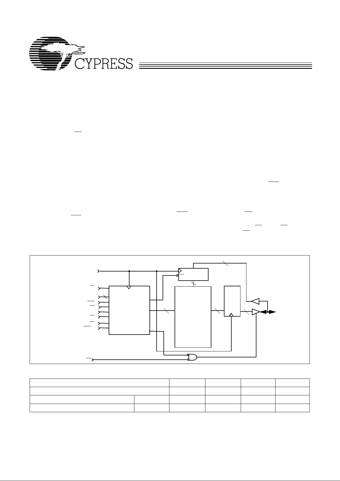
CLK
A
[15:0]
CEN
WE
BWS
CE
1
CE
CE
2
OE
OOUTPUT
64KX
32
MEMORY
ARRAY
CLK
Logic Block Diagram
DQ
[31:0]
Data-In REG.
Q
D
CE
CONTROL
and WRITE
LOGIC
3
[3:0]
REGISTERS
and LOGIC
ADV/LD
32
32
32
16
16
32
Selection G uide
7C1334-133 7C1334-100 7C1334-80 7C1334-50
Maximum Access Time (ns) 4.2 5.0 7.0 10
Maximum Operating Curr ent (mA) Commercial 400 360 310 260
Maximum CMOS Standby Current (mA) Commercial 5.0 5.0 5.0 5.0
CY7C1334
2
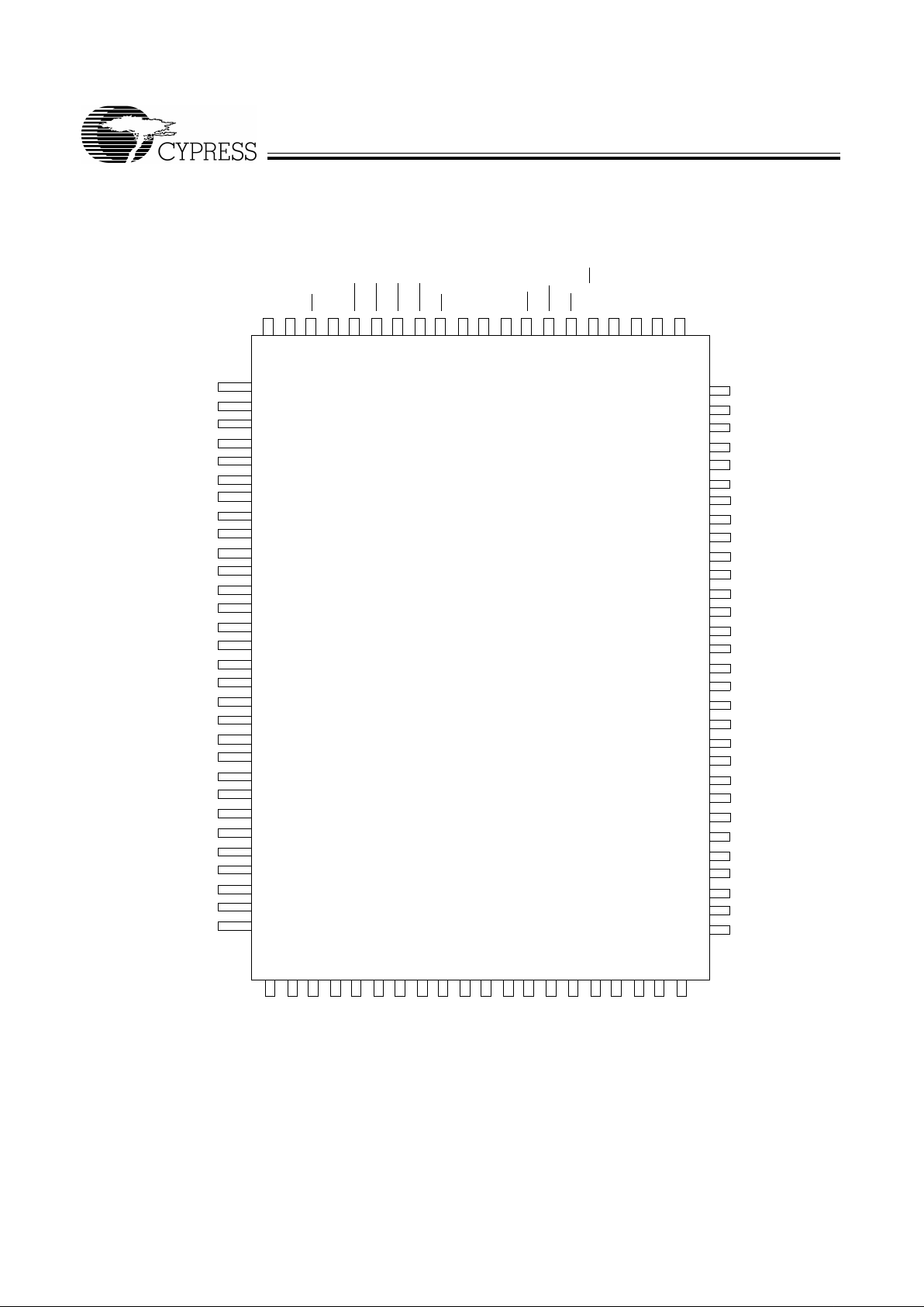
Pin Configuration
A5A4A3A2A1A
0
DNU
DNU
V
SS
V
DD
DNU
A
10A11A12A13A14
NC
NC
DQ
15
DQ
14
V
DDQ
V
SSQ
DQ
13
DQ
12
DQ
11
DQ
10
V
SSQ
V
DDQ
DQ
9
DQ
8
V
SS
VDD
V
DD
DQ
7
DQ
6
V
DDQ
V
SSQ
DQ
5
DQ
4
DQ
3
DQ
2
V
SSQ
V
DDQ
DQ
1
DQ
0
NC
NC
DQ
16
DQ
17
V
DDQ
V
SSQ
DQ
18
DQ
19
DQ
20
DQ
21
V
SSQ
V
DDQ
DQ
22
DQ
23
V
DDQ
V
DD
V
DD
V
SS
DQ
24
DQ
25
V
DDQ
V
SSQ
DQ
26
DQ
27
DQ
28
DQ
29
V
SSQ
V
DDQ
DQ
30
DQ
31
NC
A6A7CE1CE2BWS3BWS2BWS1BWS0CE3VDDVSSCLK
WE
CEN
OE
A8A
9
1
2
3
4
5
6
7
8
9
10
11
12
13
14
15
16
17
18
19
20
21
22
23
24
25
26
27
28
29
30
31323334353637383940414243444546474849
50
80
79
78
77
76
75
74
73
72
71
70
69
68
67
66
65
64
63
62
61
60
59
58
57
56
55
54
53
52
51
100
99989796959493929190898887868584838281
A
15
ADV/LD
NC
MODE
DNU
NC
NC
CY7C1334
100-Pin TQFP
A
15
CY7C1334
3
Pin Definitions
Pin Number Name I/O Description
49−44,
81–82, 99,
100, 32–37
A
[15:0]
Input-
Synchronous
Address Input s used to sel ect one of the 65, 536 address locati ons. Sam pled at the
rising edge of the CLK.
96–93 BW S
[3:0]
Input-
Synchronous
Byte Write Select I nputs, activ e LOW. Qualified with WE to conduct write s to the
SRAM. Sampled on the rising edge of CLK. BWS
0
controls DQ
[7:0]
, BWS1 controls
DQ
[15:8]
, BWS2 controls DQ
[23:16]
, BWS0 controls DQ
[31:24]
.
88 WE Input-
Synchronous
Write Enable Inp ut, active LO W . Sampled on the rising edge of CLK if CEN is active
LOW. This signal must be asserted LOW to initiate a write sequen ce.
85 ADV/LD Input-
Synchronous
Advance/Load input used to advance the on-chip address counter or load a new
address. When HIGH (and CEN
is asserted LOW) the internal b urst counter is
advance d. When LOW , a new address can be loaded into the de vice f or an access.
After being deselected, ADV/LD
should be driven LO W in order to load a new
address.
89 CLK Input-Clock Clock input. Used to capture all synchron ous inputs to the de vice. CLK is qualified
with CEN
. CLK is only recogniz ed if CEN is active LOW.
98 CE
1
Input-
Synchronous
Chip Enable 1 Input, active LOW. Sampled on the rising edge of CLK. Used in
conjunction with CE
2
and CE3 to select/deselect the devi ce.
97 CE
2
Input-
Synchronous
Chip Enable 2 Input, active HIGH. Sampled on the rising edge of CLK. Used in
conjunction with CE
1
and CE3 to select/deselect the devi ce.
92 CE
3
Input-
Synchronous
Chip Enable 3 Input, active LOW. Sampled on the rising edge of CLK. Used in
conjunction with CE
1
and CE2 to select/deselect the device.
86 OE Input-
Asynchronous
Output Enable , active LO W . Combined with the synchrono us logic block i nside the
device to control the direction of the I/ O pins. Whe n LOW , the I/O pins are allo wed
to behave as out puts . When deas serted HIGH, I/O pi ns ar e three- state d, and act
as input data pins. OE
is masked during the data portion of a write sequence,
during the fir st cloc k when emerging from a desel ected stat e, and when t he de vice
has been deselected.
87 CEN Input-
Synchronous
Clock Enable Input, active LOW. When asserted LOW the clock signal is recognized by t he SRAM. When deas serted HIGH the cloc k signal i s masked . Since the
deasserting CEN
does not deselect the device, CEN can be used to extend the
previous cycle when required.
29–28,
25–22,
19–18,
13–12, 9–6,
3–2, 79–78,
75–72,
69–68, 63–62
59–56, 53–52
DQ
[31:0]
I/O-
Synchronous
Bidirectiona l Data I /O line s. As i nputs , the y f eed i nto an on- chip dat a r egiste r that
is triggered by t he rising edge of CLK. As output s, the y deliv er the data conta ined
in the memory location specified by A
[15:0]
during the previous clock rise of the
read cycle. The direction of the pins is controlled by OE
and the internal control
logic. When OE
is asserted LOW, the pins can behave as output s. When HIGH,
DQ
[31:0]
are placed in a three-st ate condition. The out puts are automatically
three-stated d uring the data po rtion of a write sequence, during the firs t clock when
emerging from a de select ed st ate , and when the device is dese lecte d, regar dl ess
of the state of OE
.
31 Mode Input
Strap Pin
Mode Input. Selec ts the burst order of the de vice. Tied HIGH select s the interleave d
burst order. Pulled LOW selects the linear burst order. Mode should not change
states during oper ation. When left float ing Mode will default HIGH, t o an interleaved
burst order.
15, 16, 41, 65,
66, 91
V
DD
Pow er Suppl y Po wer s uppl y inp uts t o the cor e of t he devi ce . Sho uld be conn ect ed to 3.3 V powe r
supply.
17, 40, 67, 90 V
SS
Ground Ground for the core of the device. Should be connected to ground of the system.
4, 11, 14, 20,
27, 54, 61, 70,
77
V
DDQ
I/O Power
Supply
Power supply for the I/O circuitry. Should be connected to a 3.3V power supply.
5, 10, 21, 26,
55, 60, 71, 76
V
SSQ
I/O Ground Ground for the I/ O circuitry. Should be connected to ground of the system.
64 NC - No Connect. Reserved for drive strength control input.

CY7C1334
4
Introduction
Functional Overview
The CY7C1334 is a synchronous-pipelined Burst SRAM designed specifically to eliminate wait states during Write-Read
transitions. All synchronous inputs pass through input registers contr olled by th e risin g edge of the c loc k. The cl oc k signal
is qualifie d with the Cl oc k Enab l e input signal (CEN
). If CEN is
HIGH, the clo ck si gnal i s n ot reco gnize d and all i nternal states
are maintained. All synchronous operations are qualified with
CEN
. All data ou tput s pass th rough out put r egist ers contr olle d
by the rising edge of the clock. Maximum access delay from
the clock rise (t
CO
) is 4.2 ns (133-MHz de vice).
Accesses can be initiated by asserting all three Chip Enables
(CE
1
, CE2, CE3) activ e a t th e risi ng edge of the clock. If clock
enable (CEN
) is activ e LO W and AD V/LD is ass erted LOW, the
address presented to the device will be latched. The access
can either be a read or write operation, depending on the status of the Write Enabl e (WE
). BWS
[3:0]
can be used to conduct
byte write operat ions.
Write operations are qualified by the Write Enable (WE
). All
writes are simpl ifi ed wit h on- chip sy nchr onou s self- tim ed write
circuitry.
Three synchronous Chip Enables (CE
1
, CE2, CE3) and an
asynchronous Output Enable (OE
) simplify depth expansion.
All operations (Reads, Writes, and Deselects) are pipelined.
ADV/LD
should be driven LOW once the device has been de-
selected in order to load a ne w addr ess f or the ne x t operat ion.
Single Read Accesses
A read access is initiated when the following conditions are
satisfied at clock rise: (1) CEN
is asserted LOW, (2) CE1, CE2,
and CE
3
are ALL asserted active, (3) the write enable input
signal WE
is deasserted HIGH, and (4) ADV/LD is asserted
LOW. The address presented to the address inputs (A
0−A15
)
is latched into the Address Register and presented to the
memory core and control logic. The control logic determines
that a read access is in progress and allows the requested
data to propagate to the input of the output register. At the
rising edge of the next clock the requested data is allowed to
propagate through the output register and onto the data bus
within 4.2 ns (133 MHz device) provided OE
is active LOW.
After the first clock of the read access the output buffers are
controlled by OE
and the internal control logic. OE must be
driven LOW in order for the device to drive out the requested
data. During the second clock, a subsequent operation
(Read/Write/De select) can be initia ted. Desel ecting the de vic e
is also pipelined. Therefore, when the SRAM is deselected at
clock rise by one of the chip enable signals, its output will
three-state follow ing the next clock rise.
Burst Read Accesses
The CY7C1334 has an on-chip burst counter that allows the
user the ability to supply a single address and conduct up to
four Reads without reasserting the address inputs. ADV/LD
must be driven LOW in order to load a new address into the
SRAM, as described in the Single Read Acce ss section abov e.
The sequence of the burst counter is determined by the MODE
input signal. A LOW input on MODE selects a linear burst
mode, a HIGH selects an interleaved burst sequence. Both
burst counters use A0 and A1 in the burst sequence, and will
wrap-around when incremented sufficiently. A HIGH input on
ADV/LD
will increment th e internal burst counter regardless of
the state of chip enables inputs or WE
. WE is latched at the
beginning of a burst cycle. Theref ore , the type of acces s (Read
or Write) is maintained throughout the burst sequence.
Single Write Accesses
A write access is initiated when the following conditions are
satisfied at cl ock ri se : (1) CEN
is asserted LO W, (2) CE1, CE2,
and CE
3
are ALL asserted active, and (3) the write signal WE
is asserted LOW. The address presente d to A
0−A15
is loaded
into the Address Register. The write signals are latched into
the C o ntrol L ogic block.
On the subsequent clock rise the data lines are automatically
three-stated r egardless of the s tate of the OE
input signal. This
allows the external logic t o present the data on DQ
0
–DQ31. In
addition, the address for the subsequent access (Read/
Write/Deselect) i s latc hed int o the Addr ess Reg ister (pr o vided
the appropriate control signals are asserted).
On the next cl oc k rise the data present ed t o DQ
0
−DQ
31
inputs
(or a subset for b yte write op erations , see W rite Cycle Des cription table for detail s) is latched into t he device a nd the write is
complete.
The data written during the Write operation is controlled by
BWS
[3:0]
signals. The CY7C1334 provides byte write capabi lity that is described in the Write Cycle Description table. Asserting the Write Enable input (WE
) with the selected Byte
Write Select ( BWS
[0:3]
) input will sele ctively wr ite to on ly the
desired byte s. Bytes not selected during a byt e write opera tion
will remain unal tered. A Synchronous self-timed write m echanism has been provided to simplify the write operations. Byte
write capability has been included in order to greatly simplify
Read/Modify/Write sequences, which can be reduced to simple byte write operations.
Because the CY7C1334 is a common I/O device, data should
not be driven into t he device whi le t he outputs are active. The
Output Enable ( OE
) can be deasserted HIGH before present -
ing d a ta to the DQ
0
−DQ
31
inputs. Doing so wi ll three- state the
output drivers. As a safety precaution, DQ
0
−DQ
31
are automatically three-stated during the data portion of a write cycle,
regardless of the state of OE
.
50, 83, 84 NC - No connects. Reserv ed for address inputs for depth e xpansion. Pins 50, 83, and
84 will be used for 128K, 256K, and 512K depths respec ti vely.
1, 30, 51, 80 NC - No connects. Reserv ed for p arity I/ O s ignals on x36 devices. Thes e input s are not
connected to the device.
38, 39, 42, 43 DNU - Do Not Use pins. These pins shou ld be l eft floating or tied to VSS.
Pin Definitions
(continued)
Pin Number Name I/O Description
 Loading...