

Datasheet CY7C1324L-80AC, CY7C1324L-50AC, CY7C1324L-117AC, CY7C1324L-100AC, CY7C1324-80AC Datasheet (Cypress Semiconductor)
...
3.3V 128K x 18 Synchronous
Cache RAM
CY7C1324
Cypress Semiconductor Corporation
• 3901 North First Street • San Jose • CA 95134 • 408-943-2600
August 4, 1999
Features
• Supports 117-MHz m icroprocessor cac he systems with
zero wait states
• 128K by 18 common I/O
• Fast clock-to-output times
—7.5 ns (117 MHz)
• T wo-bit wrap-aroun d counter supporti ng either interleaved or linear burst sequence
• Separate pro cessor and contro ller address strobe s provides direct interface with the processor and external
cache controller
• Synchronous self-timed write
• Asynchr onous output enable
• I/Os capable of 2.5–3.3V operation
• JEDEC-standard pinout
• 100-pin TQFP packag ing
• ZZ “sleep” mode
Functional Description
The CY7C1324 is a 3.3V, 128K by 18 synchronous cache
RAM designed to interface with high-speed microprocessors
with minimum glue logic. Maximum access delay from clock
rise is 7.5 ns (117-MHz version). A 2-bit on-c hip counter captures the first address in a burst and increments the address
automatically for the rest of the burst access.
The CY7C1324 allows both interleaved or linear burst sequences, selected by the MODE input pin. A HIGH input on
MODE selects an interleaved burst sequence, while a LOW
selects a linear b ur st sequenc e. Burst acc esses can be i ni tiated with the Processor Address Strobe (ADSP
) or the cache
Controller Address Strobe (ADSC
) inputs. Address advance-
ment is controlled by the Address Advancement (ADV
) input.
A synchronous sel f-t imed wri te me chanism i s pro vided to sim plify the write interface. A synchronous chip enable input and
an asynchronous output enable input provide easy control for
bank selection and output three-state control.
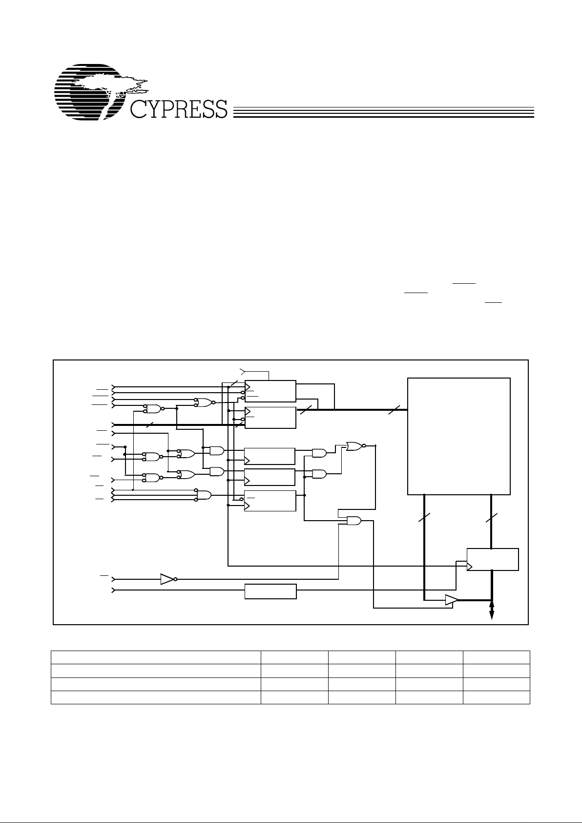
Pin
CLK
ADV
ADSC
A
[16:0]
GW
BWE
BW
0
CE
1
CE
3
CE
2
OE
ZZ
BURST
COUNTER
ADDRESS
REGISTER
INPUT
REGISTERS
128K X 18
MEMORY
ARRAY
CLK
Q
0
Q
1
Q
D
CE
CE
CLR
SLEEP
CONTROL
DQ
DQ[15:8]
BYTEWRITE
REGISTERS
DQ[7:0]
BYTEWRITE
REGISTERS
D Q
ENABLE
REGISTER
D
Q
CE
CLK
18 18
17
15
15
17
(A0,A1)
2
MODE
ADSP
Logic Block Diagram
DQ
[15:0]
BW
1
DP
[1:0]
Selection G uide
7C1324–117 7C1324–100 7C1324–80 7C1324–50
Maximum Access Time (ns) 7.5 8.0 8.5 11.0
Maximum Operat ing Current (mA) 350 325 300 250
Maximum Standb y Curr ent (mA) 1.0 1.0 1.0 1.0
Pentium is a registered trademark of Intel Corporation.
CY7C1324
2
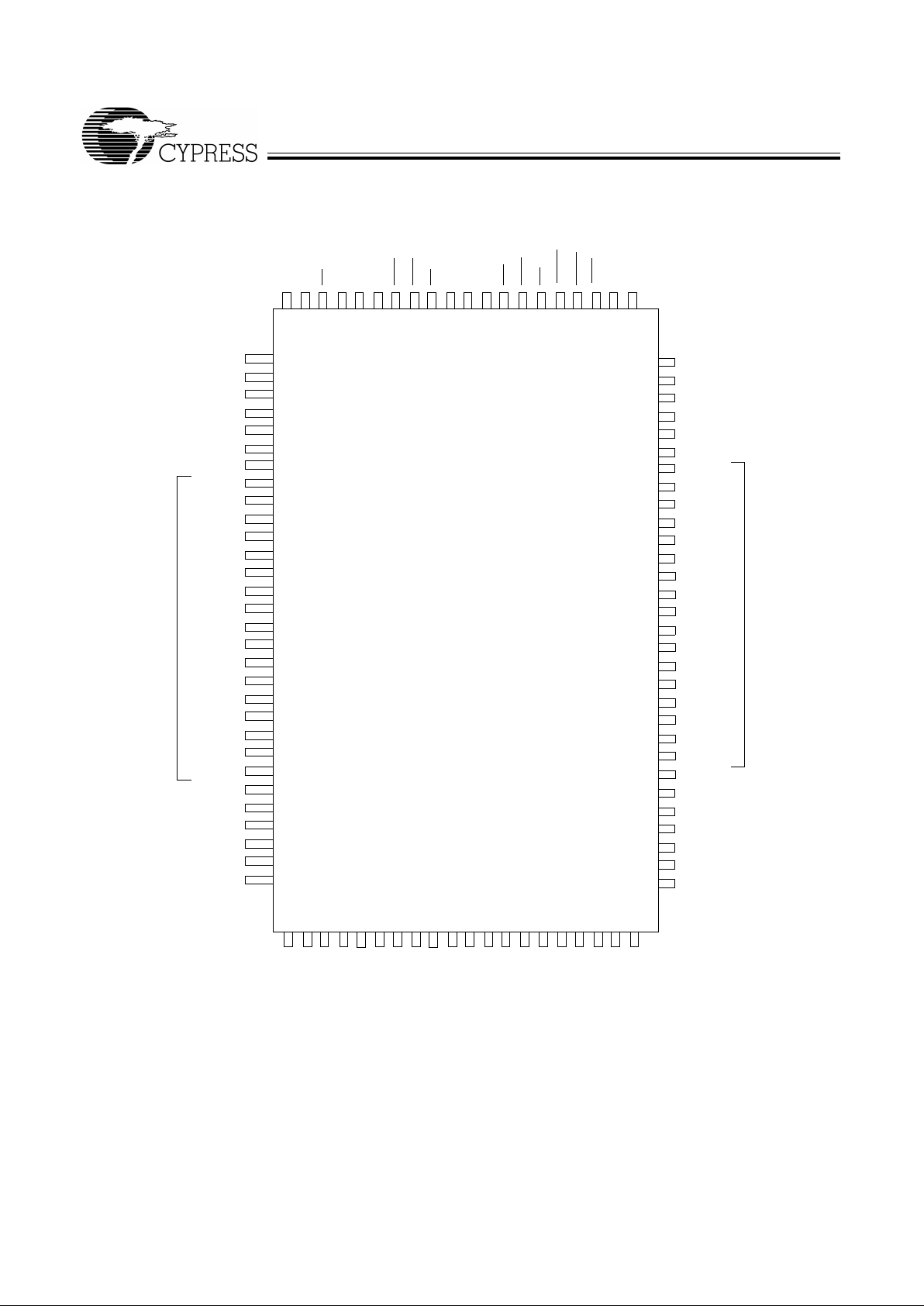
Pin Configuration
100-Lead TQFP
A5A4A3A2A1A
0
DNU
DNU
V
SS
V
DD
DNU
A
11
A12A13A14A
15
NC
A10
NC
NC
V
DDQ
V
SS
NC
DP
0
DQ
7
DQ
6
V
SS
V
DDQ
DQ
5
DQ
4
V
SS
NC
V
DD
DQ
3
DQ
2
V
DDQ
V
SS
DQ
1
DQ
0
NC
NC
V
SS
V
DDQ
NC
NC
NC
NC
NC
NC
V
DDQ
V
SS
NC
NC
DQ
8
DQ
9
V
SS
V
DDQ
DQ
10
DQ
11
NC
V
DD
NC
V
SS
DQ
12
DQ
13
V
DDQ
V
SS
DQ
14
DQ
15
DP
1
NC
V
SS
V
DDQ
NC
NC
NC
A6
A7
CE
1CE2
NC
NC
BWS
1
BWS0CE3VDDV
SS
CLKGWBWE
OE
ADSP
A8A
9
1
2
3
4
5
6
7
8
9
10
11
12
13
14
15
16
17
18
19
20
21
22
23
24
25
26
27
28
29
30
31323334353637383940414243444546474849
50
80
79
78
77
76
75
74
73
72
71
70
69
68
67
66
65
64
63
62
61
60
59
58
57
56
55
54
53
52
51
100
99989796959493929190898887868584838281
BYTE0
BYTE1
A
16
ADV
ADSC
ZZ
MODE
DNU
CY7C1324
CY7C1324
3
Functional Description
(continued)
Single Write Accesses Initiated by ADSP
This access is initiated when the following conditions are satisfi ed at clock rise: (1) CE
1
, CE2, and CE3 are all asse rted
active, and (2) ADSP
is asserted LOW. The addresses presented are loaded into the address register and the burst
counter/con trol log ic and del iv er ed to th e RAM core. The writ e
inputs (GW
, BWE, and BWS
[1:0]
) are ignored during this first
clock cycle. If the write inputs are asserted active (see Write
Cycle Descriptions table for appropriate states that indicate a
write) on the next clock rise, the appropriate data will be
latched and written into the device. Byte writes are allowed.
During byte writes, BWS
0
controls DQ
[7:0]
and DP0 while
BWS
1
controls DQ
[15:8]
and DP1. All I/Os ar e thr ee-st ate d during a byte write. Since these are common I/O devices, the
asynchronous OE
input signal must be deasser ted and the
I/Os must be three-stated prior to the presentation of data to
DQ
[15:0]
and DP
[1:0]
. As a safety precaut ion , the data li nes are
three-stated once a write cycle is detected, regardless of the
state of OE
.
Single Write Accesses Initiated by ADSC
This write access i s ini tiated when the f ol lowi ng condi t ions ar e
satisfied at clock rise: (1) CE
1
, CE2, and CE3 are all asserted
active, (2) ADSC
is asserted LOW, (3) ADSP is deasserted
HIGH, and (4) the write input signals (GW
, BWE, and BWS
[1:0]
)
indicate a write acces s. ADSC
is ignored if ADSP is active LOW .
The addresses pr esented are loaded int o the ad dress regist er ,
burst co unte r/contr ol logic and del iv ere d to t he RAM cor e. Th e
information presented to DQ
[15:0]
and DP
[1:0]
will be w ritten
into the specified address location. Byte writes are allowed,
with BWS
0
controlling DQ
[7:0]
and DP0 while BWS1 controllin g
DQ
[15:8]
and DP1. All I/Os are three-stated when a write is
detected, even a byte write. Since these are common I/O devices, the asynchronous OE
input signal must be deasserted
and the I/Os must be three-stated prior to the presentation of
data to DQ
[15:0]
and DP
[1:0]
. As a safety precaution, the data
lines are three-stated once a write cycle is detected, regardless of the state of OE
.
Single Read Accesses
A single re ad access is initiated when the following conditions
are satisfied at clock rise: (1) CE
1
, CE2, and CE3 are all as-
serted active, and (2) ADSP
or ADSC is asserted LOW (if the
access is initiated by ADSC
, the write i nputs mus t be de asserted during this first cycle). The address presented to the address inputs is latc hed into the Address Register , burst count er
/control logic and presented to the memory core. If the OE
input is asserted LOW, the requested data will be available at
the data outputs a maximum to t
CDV
after cl ock r is e. ADSP is
ignored if CE
1
is HIGH.
Burst Sequences
This family of devices provide a 2-bit wrap around burst
counter inside t he SRAM. The burst counter is fed by A
[1:0]
,
and can follow either a linear or interleaved burst order. The
burst order is determined by the state of the MODE input. A
LOW on MODE will sele ct a l inear b u rst se quence. A HIG H on
MODE will select an interleaved burst order. Leaving MODE
unconnected will cause t he device to defaul t to a interleaved
burst sequence.
Sleep Mode
The ZZ input pin is an asynchronous inpu t. Asserting a HIGH
input on ZZ pl aces the SRAM in a power conservation “sleep”
mode. Two clock cycles are required to enter into or exit from
this “sleep” mode . While in th is mode , dat a integ rity is guar an -
teed. Accesses pending when entering the “sleep” mode are
not considered valid nor is the completion of the operation
guaranteed. The device must be deselected prior to entering
the “sleep” mode. CE
1
, CE2, CE3, ADSP, and ADSC must re-
main inactive for the duration of t
ZZREC
after the ZZ input re-
turns low
T able 1. Counter Implementation for the Int el
Pentium®/80486 Processor’s Sequence
First
Address
Second
Address
Third
Address
Fourth
Address
A
X + 1, Ax
A
X + 1, Ax
A
X + 1, Ax
A
X + 1, Ax
00 01 10 11
01 00 11 10
10 11 00 01
11 10 01 00
T able 2. Counter Implementation for a Linear Sequence
First
Address
Second
Address
Third
Address
Fourth
Address
A
X + 1
, A
x
A
X + 1
, A
x
A
X + 1
, A
x
A
X + 1
, A
x
00 01 10 11
01 10 11 00
10 11 00 01
11 00 01 10
CY7C1324
4
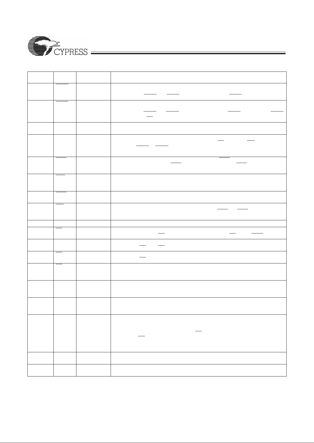
Cycle Description Table
[1, 2, 3]
Cycle Description
ADD
Used CE1CE3CE2ZZ ADSP ADSP ADV WE OE CLK DQ
Deselected Cycle, Power-down None H X X L X L X X X L-H High-Z
Deselected Cycle, Power-down None L X L L L X X X X L-H Hi gh-Z
Deselected Cycle, Power-down None L H X L L X X X X L-H High-Z
Deselected Cycle, Power-down None L X L L H L X X X L-H High-Z
Deselected Cycle, Power-down None X X X L H L X X X L-H High-Z
SNOOZE MODE, Power-down None X X X H X X X X X X HIGH-Z
READ Cycle, Begin Burst External L L H L L X X X L L-H Q
READ Cycle, Begin Burst External L L H L L X X X H L-H High-Z
WRITE Cycle, Begin Burst External L L H L H L X L X L-H D
READ Cycle, Begin Burst External L L H L H L X H L L-H Q
READ Cycle, Begin Burst External L L H L H L X H H L-H High-Z
READ Cycle, Continue Burs t Next X X X L H H L H L L-H Q
READ Cycle, Continue Burs t Next X X X L H H L H H L-H High-Z
READ Cycle, Continue Burs t Next H X X L X H L H L L-H Q
READ Cycle, Continue Burs t Next H X X L X H L H H L-H High-Z
WRITE Cycle, Continue Burst Next X X X L H H L L X L-H D
WRITE Cycle, Continue Burst Next H X X L X H L L X L-H D
READ Cycle, Suspend Burst Cur rent X X X L H H H H L L-H Q
READ Cycle, Suspend Burst Cur rent X X X L H H H H H L-H High-Z
READ Cycle, Suspend Burst Cur rent H X X L X H H H L L-H Q
READ Cycle, Suspend Burst Cur rent H X X L X H H H H L-H High-Z
WRITE Cycle, Suspend Burst Current X X X L H H H L X L-H D
WRITE Cycle, Suspend Burst Current H X X L X H H L X L-H D
Notes:
1. X=”Don't Care”, 1=Logic HIGH, 0=Logic LOW.
2. The SRAM always initiates a read cycle when ADSP
asserted, regardless of the state of GW, BWE, or BWS
[1:0].
Writes may occur only on subsequent clocks
after the ADSP
or with the assertion of ADSC. As a result, OE must be driven HIGH prior to the start of the write cycle to allow the outputs to three-state. OE
is a “Don't Care” for the remainder of the write cycle.
3. OE is asynchronous and is not sampled with the clock rise. During a read cycle DQ=High-Z when OE is inactive, and DQ=data when OE is active.
CY7C1324
5
Pin Descriptions
TQFP Pin
Number
Name I/O Description
85 ADSC Input-
Synchronous
Address Strobe from Controller, sam pled on the rising edge of CLK. When asserted
LOW, A
[16:0]
is captured in the address registers. A
[1:0]
are also load ed into the burst
counter. When ADSP
and ADSC are both asserted, only ADSP is r e c o gnized.
84 ADSP Input-
Synchronous
Address Strobe f rom Processor, sampled on the rising edge of CLK. When asserted
LOW, A
[16:0]
is captured in the address registers. A
[1:0]
are also load ed into the burst
counter . When ADSP
and ADSC are both asserted, onl y ADSP is recogniz ed. ASDP
is ignored when CE
1
is deasserted HIGH.
36, 37 A
[1:0]
Input-
Synchronous
A1, A0 Address Inputs, These i nputs feed the on-chip burst counter as the LSBs as
well as being used to access a particular memory location in the memory array.
49–44,
80–82, 99,
100,
32–35
A
[16:2]
Input-
Synchronous
Address Inputs used i n conjunction with A
[1:0]
to select one of the 128K address
locations. Sampled at the rising edge of the CLK, if CE
1
, CE2, and CE3 are sampled
active, and ADSP
or ADSC is active LOW.
94, 93 BWS
[1:0]
Input-
Synchronous
Byte Write Select Inputs, active LOW. Qualified with BWE to conduct byte writes.
Sampled on the rising edge . BWS
0
controls DQ
[7:0]
and DP0, BWS1 controls DQ
[15:8]
and DP
1
. See Write Cycle Descriptions table for further details.
83 ADV Input-
Synchronous
Advance Input use d to advance the on-chip address cou nte r . When LO W t he int ernal
burst counte r is adv an ced in a bu rst sequ ence . The b urs t sequence is se lected using
the MODE input.
87 BWE Input-
Synchronous
Byte Write Enable In put, act iv e LO W. Sampled on the rising edge of CLK. This signal
must be asserted LOW to conduct a byte write.
88 GW Input-
Synchronous
Global Write Input, active LO W . Sampled on the rising edge of CLK. Thi s signal is used
to conduct a global write, independent of the state of BWE
and BWS
[1:0]
. Global writ es
override b yte writes.
89 CLK Input-Clock Clo ck Input. Used to capture all synchronous inputs to the device.
98 CE
1
Input-
Synchronous
Chip Enable 1 Input, active LOW. Sampled on the rising edge of CLK. Used in con-
junction with CE
2
and CE3, to select/desele ct the device. CE1 gates ADSP.
97 CE
2
Input-
Synchronous
Chip Enable 2 Input, act ive HIGH. Sampled on the rising edge of CLK. Used in con-
junction with CE
1
and CE3 to select/deselect the device.
92 CE
3
Input-
Synchronous
Chip Enable 3 Input, active LOW. Sampled on the rising edge of CLK. Used in con-
junction with CE
1
and CE2 to select/d eselect the de vice.
86 OE Input-
Asynchronous
Output Enabl e, async hronous input, a ctive LOW. Controls the di rection of the I/ O pins .
When LOW, the I/O pins behave as outputs. When deasserted HIGH, I/O pins are
three-stated, and act as input data pins.
64 ZZ Input-
Asynchronous
Snooze Input. Active HIGH a synchronous. When HIGH, the de vice enters a low-power
standby mo de in which all other inputs are ignored, but the data i n the memory arra y
is maintained. Leaving ZZ floating or NC will default the device into an active state.
31 MODE - Mode Input. Selects the bur st or der of the device. Tied HIGH selects the interleaved
burst order . Pulled LOW select s the linear burst or der. When left fl oating or NC, defaul ts
to interleaved burst order.
23, 22, 19,
18, 13, 12,
9, 8, 73,
72, 69, 68,
63, 62, 59,
58
DQ
[15:0]
I/O-
Synchronous
Bidirectional Data I/O lines. As inputs, they feed into an on-chip data register that is
triggered by the rising edge of CLK. As output s , the y d elive r t he data co ntaine d in the
memory location specified by A
[17:0]
during the prev ious clock rise of the read cycle.
The direction of the pins is controlled by OE
in conjunction with the internal control
logic. When OE
is asserted LOW, the pins behave as outputs. When HIGH, DQ
[15:0]
and DP
[1:0]
are placed in a three-state condition. The outputs are automatically
three-stated when a WRITE cycle is detected.
74, 24 DP
[1:0]
I/O-
Synchronous
Bidirectional Data Parity lines. These behav e identical to DQ
[15:0]
described above.
These signals can be used as parity bits for bytes 0 and 1 respectively.
15, 41, 65, 91V
DD
Po wer Supply Power supply inputs to the core of t he device. Should be connected to 3.3V power
supply.

CY7C1324
6
Maximum Ratings
(Above which the useful life may be impaired. For user guidelines, not tested.)
Storage Temperature ........ .. ............ ............ .–65
°
C to +150°C
Ambient Temperature with
Power Applied...............................................–55
°
C to +125°C
Supply Voltage on V
DD
Relative to GND..... .......... .–0.5V to +4.6V
DC V oltage Applied to Outputs
in High Z State
[5]
........ ........ ... .... ....... .... ... .... ......–0.5V to VDD + 0.5V
DC Input Voltage
[5]
........ ....... .... .... ....... ... .... .... ..–0.5V to VDD + 0.5V
Curre n t in to Out p ut s (L OW )......................................... 20 mA
Static Discharge Voltage .......... ................................ >2001V
(per MIL-STD-883, Method 3015)
Latch-Up Current............. .. ...................... ............... >200 mA
Notes:
4. When a write cycle is detected, all I/Os are three-stated, even during byte writes.
5. Minimum voltage equals –2.0V for pulse durations of less than 20 ns.
6. T
A
is the case temper atu re.
5, 10, 17,
21, 26, 40,
55, 60, 67,
71, 76, 90
V
SS
Ground Ground for the device. Shoul d be connected to ground of the sy stem.
4, 11, 20,
27, 54, 61,
70, 77
V
DDQ
I/O Power
Supply
Pow er supply for the I/O ci rcuit ry. Should be connected to a 2.5 or 3.3V power suppl y.
1–3, 6, 7,
14, 16, 25,
28–30,
50–53, 56,
57, 66, 75,
78, 79,
95–96
NC - No connects.
38, 39, 42, 43DNU - Do not use pins. Should be left unconnected or tied LOW.
Pin Descriptions
TQFP Pin
Number
Name I/O Description
Write Cycle D escriptio n s
[1, 2, 3, 4]
Function GW BWE BWS
1
BWS
0
Read 1 1 X X
Read 1011
Write Byte 0 - DQ
[7:0]
and DP
0
1010
Write Byte 1 - DQ
[15:8]
and DP
1
1001
Write All Bytes 1000
Write All Bytes 0 X X X
ZZ Mode Electrical Characteristics
Parameter Description Test Conditions Min Max Unit
I
DDZZ
Snooze mode standb y current ZZ > V
DD
− 0.2V 10 mA
t
ZZS
Device operation to ZZ ZZ > VDD − 0.2V 2t
CYC
ns
t
ZZREC
ZZ recovery time ZZ < 0.2V 2t
CYC
ns
Operating Range
Range
Ambient
Temperature
[6]
V
DD
V
DDQ
Com’l 0°C to +70°C 3.135V to 3.6V 2.375V to V
DD

CY7C1324
7
Electrical Characteristics
Over the Operating Range
Parameter Description Test Conditions
7C1324
UnitMin. Max.
V
OH
Output HIGH Voltage V
DDQ
= 3.3V , VDD = Min., I
OH
= –4.0 mA 2.4 V
V
DDQ
= 2.5V , VDD = Min., I
OH
= –2.0 mA 1.7 V
V
OL
Output LOW Voltage V
DDQ
= 3.3V , VDD = Min., I
OL
= 8.0 mA 0.4 V
V
DDQ
= 2.5V , VDD = Min., I
OL
= 2.0 mA 0.7 V
V
IH
Input HIGH Voltage 1.7 VDD +
0.3V
V
V
IL
Input LOW Voltage
[5]
–0.3 0.8 V
I
X
Input Load Current
(except ZZ and MODE)
GND ≤ VI ≤ V
DDQ
−11µA
Input Current of MODE Input = V
SS
–30 µA
Input = V
DDQ
5 µA
Input Current of ZZ Input = V
SS
–5 µA
Input = V
DDQ
30 µA
I
OZ
Output Leakage Curren t GND ≤ VI ≤ V
DD ,
Output Disabled –55µA
I
OS
Output Short Circuit Current
[7]
VDD=Max., V
OUT
=GND –300 mA
I
DD
V
DD
Operating Supply Current VDD=Max., Iout=0mA,
f=f
MAX
=1/t
CYC
.
8.5-ns cycle, 117 MHz 325 mA
10-ns cycle, 100 MHz 300 mA
11-ns cycle, 90 MHz 275 mA
20-ns cycle, 50 MHz 225 mA
I
SB1
Automatic CE Power-Down
Current—TTL Inputs
Max. VDD, Device Deselected,
V
IN
≥ VIH or VIN ≤ VIL,
f=f
MAX,
inputs switching
8.5-ns cycle, 117 MHz 35 mA
10-ns cycle, 100 MHz 30 mA
11-ns cycle, 90 MHz 25 mA
20-ns cycle, 50 MHz 20 mA
I
SB2
Automatic CE Power-Down
Current — CMOS Inputs
Max. VDD, Device Deselected,
V
IN
≥ VDD –0.3V or VIN ≤ 0.3V, f=0,
inputs static
All speeds 10 mA
I
SB3
Automatic CE Power-Down
Current—CMOS Inputs
Max. VDD, Device Deselected,
V
IN
≥ V
DDQ
- 0.3V or VIN ≤ 0.3V,
f=f
MAX,
inputs s witc hing
8.5-ns cycle, 117 MHz 10 mA
10-ns cycle, 100 MHz 10 mA
11-ns cycle, 90 MHz 10 mA
20-ns cycle, 50 MHz 10 mA
I
SB4
Automati c C E
Po wer-Down Curre nt — TTL Inputs static, F=0
Max. VDD, Device Deselected,
V
IN
≥ VIH or VIN ≤ VIL,
f=0, inputs sta tic
All speeds 18 mA
Capacitance
[8]
Parameter Description Test Conditions Max. Unit
C
IN
Input Capacitance TA = 25°C, f = 1 MHz,
V
DD
= 5.0V
4pF
C
I/O
I/O Capacitance 4 pF
Notes:
7. Not more than one output should be shorted at one time. Duration of the short circuit should not exceed 30 seconds.
8. Tested initially and after any design or process changes that may affect these parameters.

CY7C1324
8
AC Test Loads and Waveforms
[10]
2.5V
GND
90%
10%
90%
10%
≤
2.5 ns
≤
2.5 ns
OUTPUT
R1
R2
5pF
INCLUDING
JIG AND
SCOPE
(a) (b)
ALL INPUT PULSES
1324–3
1324–4
OUTPUT
R
L
=50
Ω
Z0=50
Ω
V
L
=1.5V
2.5V
[9]
Switchin g C h ar acteristic s
Over the Operating Range
[10]
Parameter Description
-117 -100 -90 - 50
Min. Max. Min. Max. Min. Max. Min. Max. Unit
t
CYC
Clock Cycle Tim e 8.5 10 11 20 ns
t
CH
Clock HIGH 3.0 4.0 4.5 4.5 ns
t
CL
Clock LOW 3.0 4.0 4.5 4.5 ns
t
AS
Address Set-Up Before CLK Rise 2.0 2.0 2.0 2.0 ns
t
AH
Address Hold After CLK Rise 0.5 0.5 0.5 0.5 ns
t
CDV
Data Output Valid After CLK Rise 7.5 8.0 8.5 11.0 ns
t
DOH
Data Output Hold After CLK Rise 2.0 2.0 2.0 2.0 ns
t
ADS
ADSP, ADSC Set-Up Before CLK Rise 2.0 2.0 2.0 2.0 ns
t
ADH
ADSP, ADSC Hold After CLK Rise 0.5 0.5 0.5 0.5 ns
t
WES
BWS
[1:0]
, GW,BWE Set -Up B efor e CLK Ri s e 2 .0 2.0 2.0 2.0 ns
t
WEH
BWS
[1:0]
, GW,BWE Hold After CLK Rise 0.5 0.5 0.5 0.5 ns
t
ADV S
ADV Set-Up Before CLK Rise 2.0 2.0 2.0 2.0 ns
t
ADV H
ADV Hold After CLK Rise 0.5 0.5 0.5 0.5 ns
t
DS
Data Input Set-Up Before CLK Rise 2.0 2.0 2.0 2.0 ns
t
DH
Data Input Hold After CLK Rise 0.5 0.5 0.5 0.5 ns
t
CES
Chip Enable Set-Up 2.0 2.0 2.0 2.0 ns
t
CEH
Chip Enable Hold After CLK Rise 0.5 0.5 0.5 0.5 ns
t
CHZ
Clock to High-Z
[11,12]
3.5 3.5 3.5 3.5 ns
t
CLZ
Clock to Lo w-Z
[11,12]
0000ns
t
EOHZ
OE HIGH to Output High-Z
[11,13]
3.5 3.5 3.5 3.5 ns
t
EOLZ
OE LOW to Output Low-Z
[11,13]
0000ns
t
EOV
OE LOW to Output Valid 3.5 3.5 3.5 3.5 ns
Notes:
9. R1=1667Ω and R2=1538Ω for I
OH/IOL
= –4/8mA, R1=521Ω and R2=481Ω for IOH/IOL= –2/2mA.
10. Unless otherwise noted, test conditions assume signal transition time of 2.5ns or less, timing reference levels of 1.25V, input pulse levels of 0 to 2.5V, and
output loading of the specified I
OL/IOH
and load capacita nce. S ho wn in (a) an d (b) of A C t est loads .
11. t
CHZ
, t
CLZ
, t
EOHZ
, and t
EOLZ
are specified with a load capac itance o f 5 pF as i n pa rt (b) of AC Test Loads. Transition is measured ± 200 mV from stead y-state vol tag e.
12. At any given voltage and temperature, t
CHZ
(max) is less t han t
CLZ
(min).
13. This parameter is sampled and not 100% tested.

CY7C1324
9
Timing Diagrams
Writ e C ycle Ti m i n g
[14, 15]
Note:
14. WE
is the combination of BWE, BW
[3:0]
and GW to define a write cycle (see Write Cycle Descriptions table).
15. WDx stands for Write Data to Address X.
ADSP
CLK
ADSC
ADV
ADD
CE
1
OE
GW
WE
CE
2
CE
3
1a
Data-
In
t
CYC
t
CH
t
CL
t
ADS
t
ADH
t
ADS
t
ADH
t
ADVS
t
ADVH
WD1
WD2
WD3
t
AH
t
AS
t
WS
t
WH
t
WH
t
WS
t
CES
t
CEH
t
CES
t
CEH
t
CES
t
CEH
2b
3a
1a
S in gle Write
Burst Write
Unselected
ADSP ignored with CE1 inactive
CE
1
masks ADSP
= DON’T CARE
= UNDEFINED
Pipelined Write
2a
2c 2d
t
DH
t
DS
High-Z
High-Z
Unselected with CE
2
ADV Must Be Inactive for ADSP Write
ADSC initiated write

CY7C1324
10
Read Cycle Timing
[14, 16]
Note:
16. RDx stands for Read Data from Address X.
Timing Diagrams
(continued)
ADSP
CLK
ADSC
ADV
ADD
CE
1
OE
GW
WE
CE
2
CE
3
2a
2c
1a
Data Out
t
CYC
t
CH
t
CL
t
ADS
t
ADH
t
ADS
t
ADH
t
ADVS
t
ADVH
RD1
RD2
RD3
t
AH
t
AS
t
WS
t
WH
t
WH
t
WS
t
CES
t
CEH
t
CES
t
CEH
t
CES
t
CEH
t
CDV
t
EOV
2b
2c
2d
3a
1a
t
OEHZ
t
DOH
t
CLZ
t
CHZ
Single Read
Burst Read
Unselected
ADSP
ignored with CE1 inactive
Suspend Burst
CE
1
masks ADSP
= DON’T CARE
= UNDEFINED
Pipelined Read
ADSC initiated read
Unselected with CE
2

CY7C1324
11
Timing Diagrams
(continued)
In/Out
A
t
AH
t
AS
= DON’T CARE
= UNDEFINED
WE is the combination of BWE, BWS
[1:0]
and GW to def ine a write cycle (see Write C ycle Definitio ns table).
t
CLZ
t
CHZ
CE is the combination of CE2 and CE3. All chip select s need to be active in order to select
the device. RAx stands for Read Address X, WA stands for Write Address X, Dx sta nds for Data-in X,
t
DOH
CLK
ADD
WE
CE1
Data
B C
D
ADSP
ADSC
ADV
CE
OE
Q(A)
Q(B)
Q
(B+1)
Q
(B+2)
Q
(B+3)
Q(B) D(C)
D
(C+1)D(C+2)D(C+3)
Q(D)
t
CYC
t
CH
t
CL
t
ADS
t
ADH
t
ADS
t
ADH
t
ADVH
t
ADVS
t
CEH
t
CEH
t
CES
t
CES
t
WEH
t
WES
t
CDV
READ/WRITE Timing
Device originally
deselected
ADSP ignored
with CE1
HIGH
t
EOHZ
Qx stands for Data-out X.

CY7C1324
12
Pipeline Timing
Timing Diagrams
(continued)
A
t
AS
= DON’T CARE
= UNDEFINED
t
CLZ
t
CHZ
CE is the combination of CE2 and CE3. All chip selects nee d to be active in order to select
the device. RAx stands for Read Address X, WAx stands for Write Address X, Dx stands for Data-i n X,
t
DOH
CLK
ADD
WE
CE
1
Data
B
ADSP
ADSC
ADV
CE
OE
Q(A)
Q(B)
Q(D)
D(C)
D (E) D (F)
D (G)
t
CYC
t
CH
t
CL
t
ADS
t
ADH
t
CEH
t
CES
t
WEH
t
WES
t
CDV
Device or iginally
deselected
ADSP ignored
with CE
1
HIGH
Qx stands for Data-out X.
C
D
Q(C)
EF
GH
D (H)

CY7C1324
13
Timing Diagrams
(continued)
OE
three-state
I/Os
t
EOHZ
t
EOV
t
EOLZ
OE Switching Waveforms

CY7C1324
14
Notes:
17. Device must be deselected when entering ZZ mode. See Cycle Description table for all possible signal conditions to deselect the device.
18. I/Os are in three-state when exiting ZZ sleep mode.
Timing Diagrams
(continued)
ADSP
CLK
ADSC
CE
1
CE
3
LOW
HIGH
ZZ
t
ZZS
t
ZZREC
I
CC
ICC(active)
Three-state
I/Os
ZZ Mode Timing
[17 ,18
CE
2
I
CCZZ
HIGH

CY7C1324
© Cypress Semiconductor Corporation, 1999. The information contained herein is subject to change without notice. Cypress Semiconductor Corporation assumes no responsibility for the use
of any circuitry other than circuitry embodied in a Cypress Semiconductor product. Nor does it con vey or imply any license under patent or other rights. Cypress Semiconductor does not authorize
its products for use as critical components in life-support systems where a malfunction or failure may reasonably be expected to result in significant injury to the user. The inclusion of Cypress
Semiconductor products in life-support systems application implies that the manufacturer assumes all risk of such use and in doing so indemnifies Cypress Semiconductor against all charges.
Document #: 38–00651–A
Ordering Info rmation
Speed
(MHz) Ordering Code
Package
Name Pac kage Type
Operating
Range
117 CY7C1324–117AC A101 100-Lead Thin Quad Flat Pac k Commercial
100 CY7C1324–100AC A101 100-Lead Thin Quad Flat Pac k Commercial
80 CY7C1324–80AC A101 100-Lead Thin Quad Flat P ack Commercial
50 CY7C1324–50AC A101 100-Lead Thin Quad Flat P ack Commercial
Package Diagram
100-Pin Thin Plastic Quad Flat pack (14 x 20 x 1.4 mm) A101
51-85050-A
 Loading...