

Cypress Semiconductor CY7C1316V18-200BZC, CY7C1316V18-167BZC, CY7C1320V18-300BZC, CY7C1320V18-250BZC, CY7C1320V18-200BZC Datasheet
...
PRELIMINARY
18-Mb DDR-II SRAM Two-word
Burst Architecture
CY7C1316V18
CY7C1318V18
CY7C1320V18
Cypress Semiconductor Corporation • 3901 North First Street • San Jose • CA 95134 • 408-943-2600
Document #: 38-05177 Rev. *A Revised July 31, 2002
Features
• 18-Mb density (2M x 8, 1M x 18, 512K x 36)
—Supports concurrent transactions
• 250-MHz clock for high vandwidth
• Two-word burst for reducing address bus frequency
• Double Data Rate (DDR) interfaces (data t ransferred at
500 MHz) @ 250 MHz
• Two input cloc ks (K and K
) for precise DDR timing
—SRAM uses rising edges only
• Two output clocks (C and C
) accounts for clock skew
and flight time mismatches
• Echo clocks (CQ and CQ
) simplify data ca pture in high
speed systems
• Synchronous internally self-timed writes
• 1.8V core power supply with HSTL inputs and outputs
• Variable drive HSTL output buffers
• Expanded HSTL output voltage (1.4V–V
DD
)
• 13x15 mm 1.0-mm pit ch fBGA p ackage, 1 65 ball (1 1x1 5
matrix)
•JTAG interface
• On-chip Delay Lock Loop (DLL)
Configurations
CY7C1316V18 – 2M x 8
CY7C1318V18 – 1M x 18
CY7C1320V18 – 512K x 36
Functional Description
The CY7C1316V18/CY7C1318V18/CY7C1320V18 are 1.8V
Synchronous Pipelined SRAM equipped with DDR-II (Double
Data Rate) architecture. The DDR-II consists of an SRAM core
with advanced synchronous peripheral circuitry and a 1-bit
burst counter. Addresses for Read and Write are latched on
alternate rising edges of the input (K) clo ck.Write data is regi stered on the rising edges of both K and K
. Read data is d riven
on the rising edges of C and C
if provided, or on the rising ed ge
of K and K
if C/C are not provided. Each address location is
associated with two 8-bit words in the case of CY7C1316V18
that burst sequentially into or out of the device. The burst
counter always starts with a “0” internally in the case of
CY7C1316V18. On CY7C1318V18 and CY7C1320V18, the
burst counter takes in the least significant bit of the external
address and bursts two 18-bit words in the case of
CY7C1318V18 and two 36-bit words in the case of
CY7C1320V18 sequentially into or out of the device.
Asynchronous inputs include impedance match (ZQ).
Synchronous dat a outpu ts (Q, shari ng the sa me phy sica l pins
as the data in puts D) are ti ghtly matched to th e two output echo
clocks CQ/CQ
, eliminat ing the nee d for separ ately ca pturing
data from each individual DDR SRAM in the system d esign.
Output data cl ocks (C/C
) enable maximum system clocking
and data synchr onization flexibili ty.
All synchronous inp ut s pa ss thro ugh inp ut regis ters c ont rolled
by the K or K
input clocks. All data o utputs pa ss through output
registers controlled by the C or C
input clocks. Writes are
conducted with on-chip synchronous self-timed writ e circuitry.
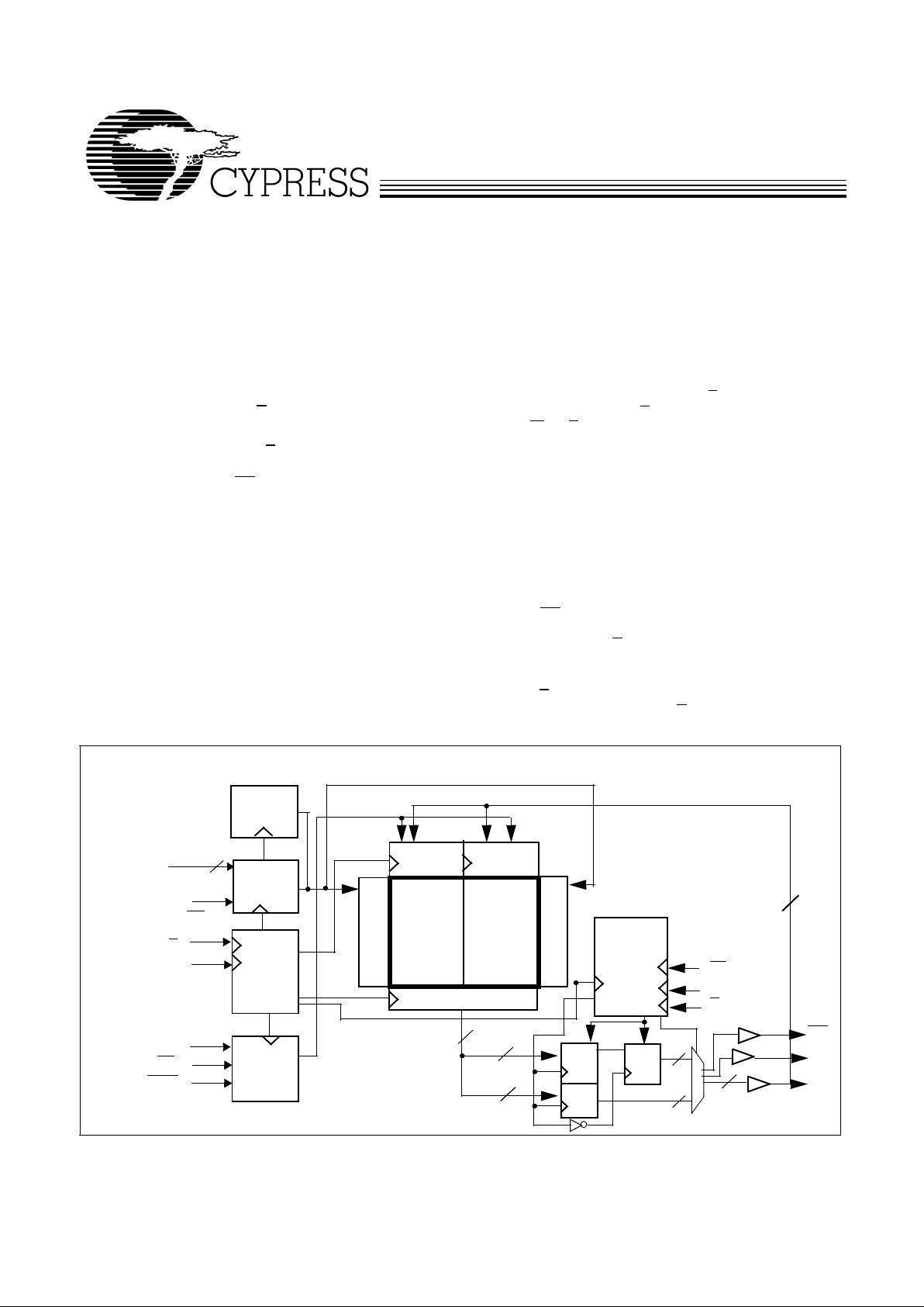
Logic Block Diagram (CY7C1316V18)
CLK
A
(19:0)
Gen.
K
K
Control
Logic
Address
Register
Read Add. Decode
Read Data Reg.
R/W
DQ
[7:0]
Output
Logic
Reg.
Reg.
Reg.
8
8
16
8
BWS
[1:0]
V
REF
Write Add. Decode
8
C
C
8
LD
Control
Burst
Logic
20
1M x 8 Array
1M x 8 Array
Write
Reg
Write
Reg
CQ
CQ
R/W
PRELIMINARY
CY7C1316V18
CY7C1318V18
CY7C1320V18
Document #: 38-05177 Rev. *A Page 2 of 24
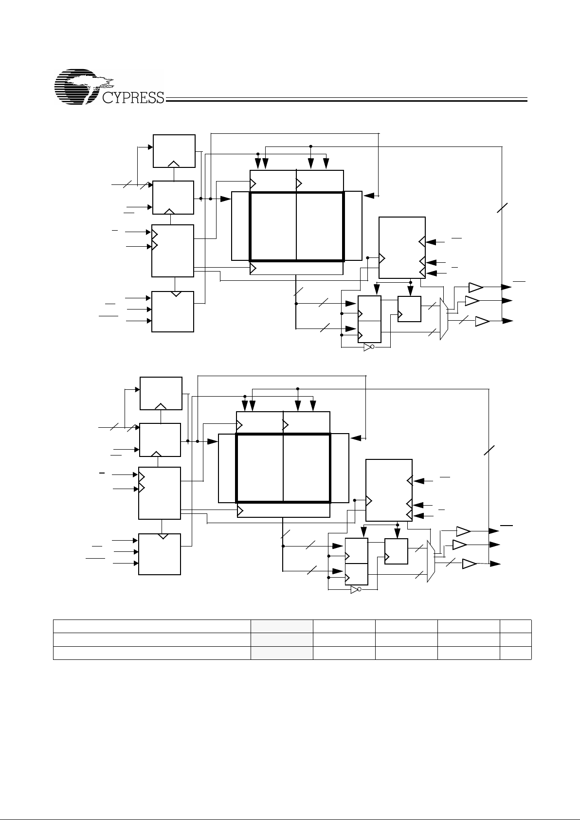
Logic Block Diagram (CY7C1318V18)
CLK
A
(19:0)
Gen.
K
K
Control
Logic
Address
Register
Read Add. Decode
Read Data Reg.
R/W
DQ
[17:0]
Output
Logic
Reg.
Reg.
Reg.
18
18
36
18
BWS
[1:0]
V
REF
Write Add. Decode
18
20
C
C
18
LD
Control
Burst
Logic
A
(0)
A
(19:1)
19
512K x 18 Array
512K x 18 Array
Write
Reg
Write
Reg
CQ
CQ
R/W
Logic Block Diagram (CY7C1320V18)
CLK
A
(18:0)
Gen.
K
K
Control
Logic
Address
Register
Read Add. Decode
Read Data Reg.
R/W
DQ
[35:0]
Output
Logic
Reg.
Reg.
Reg.
72
36
144
36
BWS
[3:0]
V
REF
Write Add. Decode
72
19
C
C
36
LD
Control
Burst
Logic
A
(0)
A
(18:1)
18
256K x 36 Array
256K x 36 Array
Write
Reg
Write
Reg
CQ
CQ
36
R/W
Selection Guide
[1]
300 MHz 250 MHz 200 MHz 167 MHz Unit
Maximum Operating Frequency 300 250 200 167 MHz
Maximum Operating Current TBD TBD TBD TBD mA
Note:
1. Shaded cells indicate advanced information.
PRELIMINARY
CY7C1316V18
CY7C1318V18
CY7C1320V18
Document #: 38-05177 Rev. *A Page 3 of 24
Pin Configurations
CY7C1316V18 (2M x 8) - 11 x 15 FBGA
2345671
A
B
C
D
E
F
G
H
J
K
L
M
N
P
R
A
CQ
NC
NC
NC
NC
DOFF
NC
V
SS
/72M A BWS
1
KR/W
NC
NC NC
NC
NC
NC
TDO
NC
NC
NC
NC
NC
NC
TCK
NC
NC
A NC K BWS
0
V
SS
AAA
NC V
SS
V
SS
V
SS
V
SS
V
DD
A
V
SS
V
SS
V
SS
V
DD
DQ4
NC
V
DDQ
NC
NC
NC
NC
DQ7
A
V
DDQ
V
SS
V
DDQ
V
DD
V
DD
DQ5 V
DDQ
V
DD
V
DDQ
V
DD
V
DDQ
V
DD
V
SS
V
DD
V
DDQ
V
DDQ
V
SS
V
SS
V
SS
V
SS
A
AC
V
SS
A
A
A
NC V
SS
NC V
SS
NC
NC
V
REF
V
SS
V
DD
V
SS
V
SS
A
V
SS
C
NC
DQ6
NC
NC
NC
V
DD
A
891011
NC
AV
SS
/36MLD
CQ
A NC NC DQ3
V
SS
NC NC NC
NC
V
SS
NC
DQ2
NC
NC
NC
V
REF
NC
NC
V
DDQ
NC
V
DDQ
NC NC
V
DDQ
V
DDQ
V
DDQ
NCV
DDQ
NC
DQ1
NC
V
DDQ
V
DDQ
NC
V
SS
NC NC
NC
TDITMS
V
SS
A
NC
A
NC
NC
NC
ZQ
NC
DQ0
NC
NC
NC
NC
A
CY7C1318V18 (1M x 18) - 11 x 15 FBGA
234 5671
A
B
C
D
E
F
G
H
J
K
L
M
N
P
R
A
CQ
NC
NC
NC
NC
DOFF
NC
V
SS
/72M A BWS
1
KR/W
NC
DQ9
NC
NC
NC
NC
TDO
NC
NC
NC
NC
NC
NC
TCK
NC
NC
A NC
K
BWS
0
V
SS
AA0A
DQ10 V
SS
V
SS
V
SS
V
SS
V
DD
A
V
SS
V
SS
V
SS
V
DD
DQ11
NC
V
DDQ
NC
DQ14
NC
DQ16
DQ17
A
V
DDQ
V
SS
V
DDQ
V
DD
V
DD
DQ13 V
DDQ
V
DD
V
DDQ
V
DD
V
DDQ
V
DD
V
SS
V
DD
V
DDQ
V
DDQ
V
SS
V
SS
V
SS
V
SS
A
AC
V
SS
A
A
A
NC V
SS
NC V
SS
DQ12
NC
V
REF
V
SS
V
DD
V
SS
V
SS
A
V
SS
C
NC
DQ15
NC
NC
NC
V
DD
A
891011
DQ0
AV
SS
/36MLD
CQ
A NC
NC
DQ8
V
SS
NC DQ7 NC
NC
V
SS
NC
DQ6
NC
NC
NC
V
REF
NC
DQ3
V
DDQ
NC
V
DDQ
NC DQ5
V
DDQ
V
DDQ
V
DDQ
NCV
DDQ
NC
DQ4
NC
V
DDQ
V
DDQ
NC
V
SS
NC NC
NC
TDITMS
V
SS
A
NC
A
NC
NC
NC
ZQ
NC
DQ2
NC
DQ1
NC
NC
A
PRELIMINARY
CY7C1316V18
CY7C1318V18
CY7C1320V18
Document #: 38-05177 Rev. *A Page 4 of 24
Pin Configurations (continued)
CY7C1320V18 (512K x 36) - 11 x 15 FBGA
2345671
A
B
C
D
E
F
G
H
J
K
L
M
N
P
R
A
CQ
NC
NC
NC
NC
DOFF
NC
V
SS
/144M NC/36M BWS
2
KR/W BWS
1
DQ27
DQ18
NC
NC
NC
TDO
NC
NC
DQ31
NC
NC
NC
TCK
NC
DQ28
A BWS
3
K
BWS
0
V
SS
AA0A
DQ19 V
SS
V
SS
V
SS
V
SS
V
DD
A
V
SS
V
SS
V
SS
V
DD
DQ20
DQ21
V
DDQ
DQ32
DQ23
DQ34
DQ25
DQ26
A
V
DDQ
V
SS
V
DDQ
V
DD
V
DD
DQ22 V
DDQ
V
DD
V
DDQ
V
DD
V
DDQ
V
DD
V
SS
V
DD
V
DDQ
V
DDQ
V
SS
V
SS
V
SS
V
SS
A
AC
V
SS
A
A
A
DQ29 V
SS
NC V
SS
DQ30
NC
V
REF
V
SS
V
DD
V
SS
V
SS
A
V
SS
C
NC
DQ33
NC
DQ35
DQ24
V
DD
A
891011
DQ0
AV
SS
/72MLD CQ
A NC
NC
DQ8
V
SS
NC DQ17 DQ7
NC
V
SS
NC
DQ6
DQ14
NC
NC
V
REF
NC
DQ3
V
DDQ
NC
V
DDQ
NC DQ5
V
DDQ
V
DDQ
V
DDQ
DQ4V
DDQ
NC
DQ13
NC
V
DDQ
V
DDQ
NC
V
SS
NC DQ1
NC
TDITMS
V
SS
A
NC
A
DQ16
DQ15
NC
ZQ
DQ12
DQ2
DQ10
DQ11
DQ9
NC
A
Pin Definitions
Pin Name I/O Pin Description
DQ
[x:0]
Input/OutputSynchronous
Data input/Output signals. In puts are sampled o n the rising edge of K and K clocks du ring valid
write operations. These pins driv e out the req uested dat a during a Read operatio n. Valid data is
driven out on the rising edge of both the C an d C
clocks during Read operations or K an d K when
in single clock mode. When the Read port is deselected, Q
[x:0]
are automatically three-stated.
CY7C1316V18 − DQ
[7:0]
CY7C1318V18 − DQ
[17:0]
CY7C1320V18− DQ
[35:0]
LD Input-
Synchronous
Synchronous load. This input is brought LOW when a bus cycle sequ ence is to be defin ed. This
definition includes address and read/writ e directio n. All transact ions opera te on a burs t of 2 data.
BWS0, BWS1,
BWS2, BWS
3
Input-
Synchronous
Byte Write Select 0, 1, 2, and 3 − active LOW. Sampl ed on the rising e dge of the K and K cl ocks
during write operations. Used to select which byte is written into the device during the current
portion of the write operations. Bytes not written remain unaltered.
CY7C1311V18 − BWS
0
controls D
[3:0]
and BWS1 controls D
[7:4]
.
CY7C1313V18 − BWS0 controls D
[8:0]
and BWS1 controls D
[17:9].
CY7C1315V18 − BWS0 controls D
[8:0]
, BWS1 controls D
[17:9]
, BWS2 controls D
[26:18]
and BWS3
controls D
[35:27]
.
All the byte writes are sampled on the same edge as the data. Deselecting a Byte Write Select
will cause the corresponding byte of data to be ignored and not written into the device.
A, A0 Input-
Synchronous
Address inputs. These address inputs are multiplexed for both Read and Write operations.
Internally, the device is organized as 2M x 8 (2 arrays each of 1M x 8) for CY7C131 6V1 8, 1M x
18 (2 arrays each of 512 K x 18 ) for CY 7C1 318 V18 a nd 5 12K x 36 (2 a rray s ea ch of 25 6K x 36 )
for CY7C1320V18.
CY7C1316V18 – Since the least significant bit of the address internally is a “0,” only 20 external
address inputs are needed to access the entire memory array.
CY7C1318V18 – A0 is the input to the burs t cou nter. These are incre me nted in a linear fas hi on
internally. 20 address inputs are nee ded to acces s the entire me mo ry array.
CY7C1320V18 – A0 is the input to the burs t cou nter. These are incre me nted in a linear fas hi on
internally. 19 address input s are nee ded to ac c ess th e en tire mem ory arra y. All the dres s inputs
are ignored when the appropriate port is deselected.
PRELIMINARY
CY7C1316V18
CY7C1318V18
CY7C1320V18
Document #: 38-05177 Rev. *A Page 5 of 24
R/W Input-
Synchronous
Synchronous Read/Write Inpu t. When LD is LOW , this input designates the access type (READ
when R/W
is HIGH, WRITE when R/W is low) for l oaded address . R/W must meet the set-up a nd
hold times around edge of K.
C Input-
Clock
Positive Output Clock Input. C is used in conjunction with C to clock out the Read data from
the device. C and C
can be used together to deskew the flight times of various devices on the
board back to the controller. See application example for further details.
C Input-
Clock
Negative Output Clock Input. C is used in conjunction with C to clock out the Read data from
the device. C and C
can be used together to deskew the flight times of various devices on the
board back to the controller. See application example for further details.
K Input-
Clock
Positive Input Clock Input. The rising edge of K is used to capture synchronous inputs to the
device and to drive out data through Q
[x:0]
when in single clock m ode . All ac c ess es are in iti ate d
on the rising edge of K.
K Input-
Clock
Negative Input Clock Input. K i s used to capture sync hronous data being pre sented to the device
and to drive out data through Q
[x:0]
when in single clock mode.
CQ Echo Clock CQ is referenced with respect to C. This is a free running clock and is synchronized to the
output clock of the QDR
TM
-II. In the single clock mode, CQ is generated with respect to K. The
timings for the echo clocks are shown in the AC timing table.
CQ Echo Clock CQ is referenced with respect to C. This is a free running clock and is synchronized to the
output clock of the QDR
TM
-II. In the single clock mode, CQ is generated with respect to K. The
timings for the echo clocks are shown in the AC timing table.
ZQ Input Output Impedance Matching Input. This input is used to tune the device ou tputs t o the sys tem
data bus impedance. Q
[x:0]
output impedance are set to 0.2 x RQ, where RQ is a resistor
connected between ZQ and ground. Alternatel y , this pi n can be connected directly to V
DD
, which
enables the minimum impedance mode. This pin cannot be connected directly to GND or left
unconnected.
DOFF Input DLL Turn Off. Connecting this pin to ground will turn off the DLL inside the device. The timings
in the DLL turned off operation will be different from those listed in this data sheet. More details
on this operation can be found in the application note, “DLL Operation in the QDR
TM
-II.”
TDO Output TDO for JTAG.
TCK Input TCK pin for JTAG.
TDI Input TDI pin for JTAG.
TMS Input TMS pin for JTAG.
NC Input No connects. Can be tied to any voltage level.
NC/36M Input Address expansion for 36M. This is not connected to the die.
NC/72M Input Address expansion for 72M. This is not connected to the die an d so can be tied to any volt age
level.
VSS/72M Input Address expansion for 72M. This must be tied LOW on the 18M SRAM.
VSS/144M Input Address expansion for 144M. This must be tied LOW on the 18M SRAM.
VSS/288M Input Address expansion for 288M. This must be tied LOW on the 18M SRAM.
V
REF
Input-
Reference
Reference V oltage Input. S tatic input used to set the reference level for HSTL inputs and Outputs
as well as A/C measurement points.
V
DD
Power Supply Power supply inputs to the core of the device. Should be connected to 1.8V power supply.
V
SS
Ground Ground for the device. Should be connected to ground of the system.
V
DDQ
Power Supply Power supply inputs for the outp uts of the device. Should be co nnected to 1.5V power sup ply .
Pin Definitions (continued)
Pin Name I/O Pin Description

PRELIMINARY
CY7C1316V18
CY7C1318V18
CY7C1320V18
Document #: 38-05177 Rev. *A Page 6 of 24
Introduction
Functional Overview
The CY7C1316V18/CY7C1318V18/CY7C1320V18 are
synchronous pipelined Burst SRAMs equipped with a DDR
interface.
Accesses are initiated on the Positive Input Clock (K). All
synchronous input ti ming is refe renced from the rising edge of
the input clocks (K and K
) and all output timing is referenced
to the output clocks (C/C
or K/K when in single clock mode).
All synchronous data inputs (D
[x:0]
) pass through input
registers controlled by the input clocks (K and K
). All
synchronous data outputs (Q
[x:0]
) pass through output
registers control led by the rising edge of the output c locks (C/C
or K/K when in single-clock mode).
All synchronous control (R/W, LD, BWS
[0:X]
) inputs pass
through input registers controlled by the rising edge of the
input clock (K ).
The following descriptions take CY7C1318V18 as an
example. However, the same is true for the other DDR-II
SRAMs, CY7C1316V18 and CY7C1320V18.
These chips utilize a Delay Lock Loop (DLL) that is designed
to function betwee n 80 MH z and the specifie d maximum clock
frequency . The DLL may be disabled by applying gro und to the
DOFF
pin.
Read Operations
Accesses are completed in a burst of two sequential 18-bit
data words. Read operations are in itiated by assertin g R/W
HIGH and LD LOW at the rising edge of the Positive Input
Clock (K). The address presented to Address inputs is stored
in the Read address registe r and the least s ignificant bit of the
address is presented to the burst counter. The burst counter
increments th e add res s in a lin ea r fashion. Following the next
K clock rise the corresponding 18-bit word of data from this
address location is driven onto the Q
[17:0]
using C as the output
timing reference. On the subs equent rising edge o f C th e next
18-bit data wo rd from the address loca tion gen erated by th e
burst counter is driven onto the Q
[17:0]
. The requested dat a will
be valid 0.35 ns from the rising edge of the output clock (C or
C
, 250-MHz device). In order to maintain the internal logic,
each read access must be allowed to complete. Read
accesses can be initiated on every rising edge of the Positive
Input Clock (K).
When the read port is dese lected, the CY7C1318V18 wil l fi rst
complete the pend ing read transa ctions. Synchrono us internal
circuitry will autom atically th ree-stat e the o utputs fol lowing the
next rising edge of the Positive Output Clock (C). This will
allow for a seamless transition between devices without the
insertion of wait states in a depth expanded memory.
Write Operations
Write operations are initiated by asserting R/W
LOW and LD
LOW at the rising edge of the Positive Input Clock (K). The
address presented to Address inputs is stored in the Write
address register and the least significant bit of the address is
presented to the burst counter. The burst counter increments
the address in a linear fashion. On the following K clock rise
the data presented to D
[17:0]
is latched and stored into the
18-bit Write Da ta regi ster provi ded BWS
[1:0]
are both asserted
active. On the subsequent rising edge of the Negative Input
Clock (K
) the information presented to D
[17:0]
is also stored
into the Write Data Register provided BWS
[1:0]
are both
asserted active. The 36 bits of data are then written into the
memory array at the specified location. Write accesses can be
initiated on every rising edge of the Positive Input Clock (K).
Doing so will pipeline the data flow such that 18 bits of data
can be transferred into the device on every rising edge of the
input clocks (K and K
).
When deselected, the write port will ignore all inputs after the
pending Write operations have been completed.
Byte Write Operations
Byte Write op erati on s a re sup po rted by the CY7C1318V18. A
write operation is initi ated as describ ed in the Write Operation
section above. The bytes that are written are determined by
BWS
0
and BWS1 which are sampled with each set of 18-bit
data word. Asserting the appropriate Byte Write Select input
during the data portion of a write will allow the data being
presented to be latched and written into the device.
Deasserting the By te Write S elect input during the data porti on
of a write will allow the data stored in the device for that byte
to remain unaltered. This feature can be used to simplify
Read/Modify/Write operations to a Byte Write operation.
Single Clock Mode
The CY7C1318V18 can be used with a single clock that
controls bot h the i nput and out put r egister s. In this m ode th e
device will re cogni ze on ly a si ngl e pair of input cloc ks (K an d
K
) that control both the input and output registers. This
operation is identical to the operation if the device had zero
skew between the K/K
and C/C clocks. All tim ing parame ter s
remain the same in this mode. To use this mode of operation,
the user must tie C and C
HIGH at power- on . Th is fu n ct ion is
a strap option and not alterable during device operation.
DDR Operation
The CY7C1318V18 enables high performance operation
through high clock frequencies (achieved through pipelining)
and double data rate mode of operation. The CY7C1318V18
requires a single No O peration (NOP) cycl e when transitioning
from a Read to a Write cycle. At higher frequencies, some
applications may require a second NOP cycle to avoid
contention.
If a Read occurs after a Write cycle, address and data for the
Write are stored in registers. The write information must be
stored because the SRAM c an not perform the last wo rd Write
to the array without conflicting with the Read. The data stays
in this register until the next Write cycle occurs. On the first
Write cycle af ter the READ (s), the st ored dat a from the earl ier
Write will be written into the SRAM array. This is called a
Posted Write.
If a Read is performed o n th e sa me address on which a Writ e
is performed in the previous cycle, the SRAM reads out the
most current data. The SRAM does this by bypassing the
memory array and reading the data from the registers.
Depth Expansion
Depth expansion requires replicating the LD
control signal for
each bank. All other control signals can be common between
banks as appropriate.
PRELIMINARY
CY7C1316V18
CY7C1318V18
CY7C1320V18
Document #: 38-05177 Rev. *A Page 7 of 24
Programmable Impedance
An external resistor, RQ, must be connected between the ZQ
pin on the SRAM and V
SS
to allow the SRAM to adjust its
output driver impedance. The value of RQ must be 5X the
value of the inten ded line impe dance driven by the SRAM, The
allowable range of RQ to guaran tee impedanc e matchi ng with
a tolerance of ±10% is between 175Ω and 350Ω
, with
V
DDQ
= 1.5V. The output impedance is adjusted every 1024
cycles to adjust for drifts in supply voltage and temperature.
Echo Clocks
Echo clocks are provided on the DDR-II to simplify data
capture on high-speed systems. Two echo clocks are
generated by the DDR-II. CQ is referenced with respect to C
and CQ
is referenced with respect to C. These are
free-running clocks and are synchronized to the output clock
of the DDR-II. In the single clock mode, CQ is generated with
respect to K and CQ
is generated with respect to K. The
timings for the echo clocks are shown in the AC Timing table.
Application Example
[2]
DQ
Add.
K/K
C/C
R/W
Add.
K/K
C/C
R/W
18
72
SRAM #1
SRAM #4
V
TERM
= V
REF
CLK/CLK (output)
DQ
LD
Add.
R/W
CLK/CLK (input)
18
2
R = 50Ω
VT = V
REF
R = 50Ω
DQ
Memory
Controller
20
20
2
LD
LD
Truth Table
[3, 4,5, 6, 7, 8]
Operation K LD R/W DQ DQ
Write Cycle:
Load address; input write data on consecutive K and K
rising
edges.
L-H L L D(A1)at K(t + 1) ↑ D(A2) at K
(t + 1) ↑
Read Cycle:
Load address; wait one cycle; read data on consecutive C
and
C rising edg es.
L-H L H Q(A1) at C
(t + 1)↑ Q(A2) at C(t + 2) ↑
NOP: No Operation L-H H X High-Z High-Z
Standby: Clock Stopped Stopped X X Previous State Previous State
Notes:
2. The above application shows 4 of CY7C1318V18 being used. This holds true for CY7C1316V18 and CY7C1320V18 as well.
3. X = “Don’t Care,” H = Logic HIGH, L = Logic LOW,
↑represents rising edge.
4. Device will power-up deselected and the outputs in a three-state condition.
5. On CY7C1318V18 and CY7C1320V18, “A1” represents address location latched by the devices when transaction was initiated and A2 represents the addresses
sequence in the burst. On CY7C1316V18, “A1” represents A + ‘0’ and A2 represents A + ‘1.’
6. “t” represents the cycle at which a read/write operation is started. t+1 and t + 2 are the first and second clock cycles succeeding the “t” clock cycle.
7. Data inputs are registered at K and K
rising edges. Data outputs are delivered on C and C rising edges, except when in single clock mode.
8. It is recommended that K = K
and C = C = HIGH when clock is stopped. This is not essential, but permits most rapid restart by overcoming transmission line
charging symmetrically.
PRELIMINARY
CY7C1316V18
CY7C1318V18
CY7C1320V18
Document #: 38-05177 Rev. *A Page 8 of 24
Burst Address Table (CY7C1318V18 and
CY7C1320V18)
First Address (External) Second Address (Internal)
X..X0 X..X1
X..X1 X..X0
Write Cycle Descriptions
(CY7C1316V18 and CY7C1318V18)
[3, 9]
BWS0BWS1KK Comments
LLL-H– During the Data portion of a Write sequence :
CY7C1316V18 − both nibbles (D
[7:0]
) are written into the device,
CY7C1318V18 − both bytes (D
[17:0]
) are written into the device.
LL– L-H During the Data portion of a Write sequence :
CY7C1316V18 − both nibbles (D
[7:0]
) are written into the device,
CY7C1318V18 − both bytes (D
[17:0]
) are written into the device.
LHL-H– During the Data portion of a Write sequence :
CY7C1316V18 − only the lo wer nibb le (D
[3:0]
) is written into th e device. D
[7:4]
will remain unalt ered,
CY7C1318V18 − only the lower byte (D
[8:0]
) is written into the device. D
[17:9]
will remain unaltered.
LH– L-H During the Data portion of a Write sequence :
CY7C1316V18 − only the lo wer nibb le (D
[3:0]
) is written into th e device. D
[7:4]
will remain unalt ered,
CY7C1318V18 − only the lower byte (D
[8:0]
) is written into the device. D
[17:9]
will remain unaltered.
HLL-H– During the Data portion of a Write sequence :
CY7C1316V18 − only th e upper nibbl e (D
[7:4]
) is written into the de vice. D
[3:0]
will remain unalt ered,
CY7C1318V18 − only the upper byte (D
[17:9]
) is written into the device. D
[8:0]
will remain unaltered.
HL– L-H During the Data portion of a Write sequence :
CY7C1316V18 − only th e upper nibbl e (D
[7:4]
) is written into the de vice. D
[3:0]
will remain unalt ered,
CY7C1318V18 − only the upper byte (D
[17:9]
) is written into the device. D
[8:0]
will remain unaltered.
HHL-H– No data is written into the devices during this portion of a write operation.
HH– L-H No data is written into the devices during this portion of a write operation.
Write Cycle Descriptions
(CY7C1320V18)
[3, 9]
BWS
0
BWS
1
BWS
2
BWS
3
KK Comments
LLLLL-H– During the Data portion o f a Write sequen ce,
all four bytes (D
[35:0]
) are written into the
device.
LLLL– L-H During the Data portion o f a Write sequen ce,
all four bytes (D
[35:0]
) are written into the
device.
LHHHL-H– During the Data po rtion of a Wri te sequence,
only the lower byte (D
[8:0]
) is written into the
device. D
[35:9]
will remain unaltered.
LHHH– L-H During the Dat a portion of a Write sequence ,
only the lower byte (D
[8:0]
) is written into the
device. D
[35:9]
will remain unaltered.
HLHHL-H– During the Data portion of a W rite sequence,
only the byte (D
[17:9]
) is written into the
device. D
[8:0]
and D
[35:18]
will remain
unaltered.
Note:
9. Assumes a Write cycle was initiated per the Write Port Cycle Description Truth T able. BWS
0
, BWS1 in the case of CY7C1316V18 and CY7C1318V18 and also
BWS
2
, BWS3 in the case of CY7C1320V18 can be altered on different portions of a write cycle, as long as the set-up and hold requirements are achieved.
 Loading...