

512K x 8 Static RAM
CY7C1049V33
Cypress Semiconductor Corporation
• 3901 North First Street • San Jose • CA 95134 • 408-943-2600
June 2, 1999
3
Features
• High speed
—t
AA
= 15 ns
• Low active power
—504 mW (max.)
• Low CMOS standby power (Commercial L version)
—1.8 mW (max.)
• 2.0V Data Retention (660 µW at 2.0V retention)
• Automat ic power-down when deselected
• TTL-compatibl e inputs and outputs
• Easy memory expansion with CE
and OE fe atures
Functional Description
The CY7C1049V33 is a high-performance CMOS Static RAM
organized as 524,288 words by 8 bits. Easy memory expan-
sion is provided by an active LO W Chip Enable (CE
), an acti ve
LOW Output Enable (OE
), and three-state drivers. Writing to
the device is accomplished by taking Chip Enable (CE
) and
Write Enable ( WE
) inputs LOW . Data on the ei ght I/ O pins ( I/O
0
through I/O7) is then written into the location specified on the
address pins (A
0
through A18).
Reading from the device is accomplished by taking Chip
Enable (CE
) and Output Enab le (OE) LO W whi le f orci ng Write
Enable (WE
) HIGH. Under these conditions, the contents of
the memory locati on specified by the address pins wil l appear
on the I/O pins.
The eight input/output pins (I/O
0
through I/O7) are placed in a
high-impedance state when the device is deselected (CE
HIGH), the outputs are disabled (OE HIGH), or during a write
operation (CE
LOW, and WE LOW).
The CY7C1049V33 is available in a standard 400-mil-wide
36-pin SOJ package with cent er power and groun d (revol utionary) pinout.
14
15
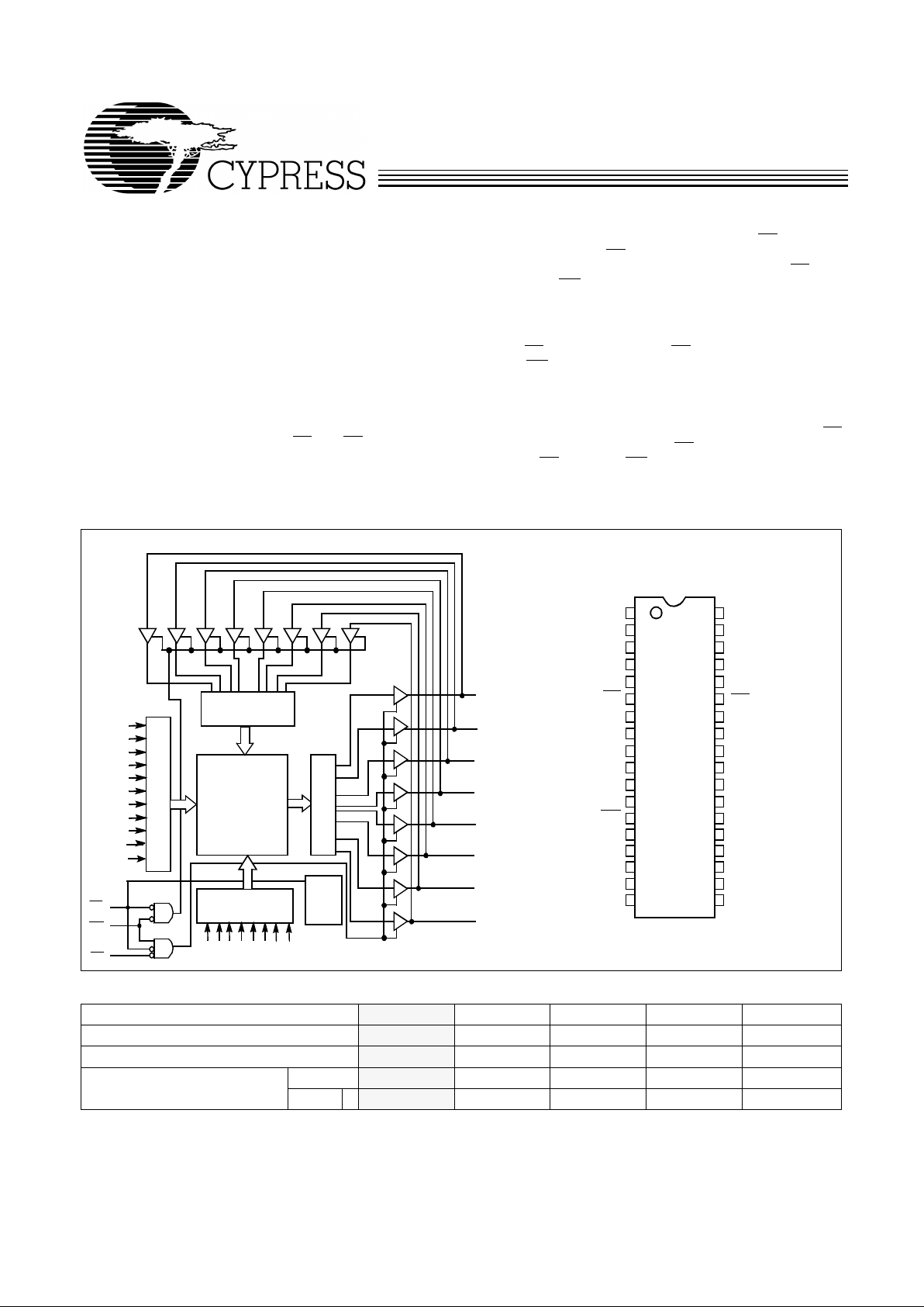
Logic Block Diagram Pin Configuration
A
1
A
2
A
3
A
4
A
5
A
6
A
7
A
8
COLUMN
DECODER
ROW DECODER
SENSE AMPS
INPUT BUFFER
POWER
DOWN
WE
OE
I/O
0
I/O
1
I/O
2
I/O
3
512K x 8
ARRAY
I/O
7
I/O
6
I/O
5
I/O
4
A
0
A
11
A13A
12
ACEA
A
16
A
17
1
2
3
4
5
6
7
8
9
10
11
14
23
24
28
27
26
25
29
32
31
30
Top View
SOJ
12
13
33
36
35
34
16
15
21
22
GND
A
1
A
2
A
3
A
4
A
5
A
6
A
7
A
8
WE
V
CC
A
18
A
15
A
12
A
14
I/O
5
I/O
4
1049V33–1
A
9
A
0
I/O
0
I/O
1
I/O
2
OE
A
17
A
16
A
13
CE
1049V33–2
A
9
A
18
18
17
19
20
GND
I/O
7
I/O3
I/O
6
V
CC
A
10
A
11
NC
NC
A
10
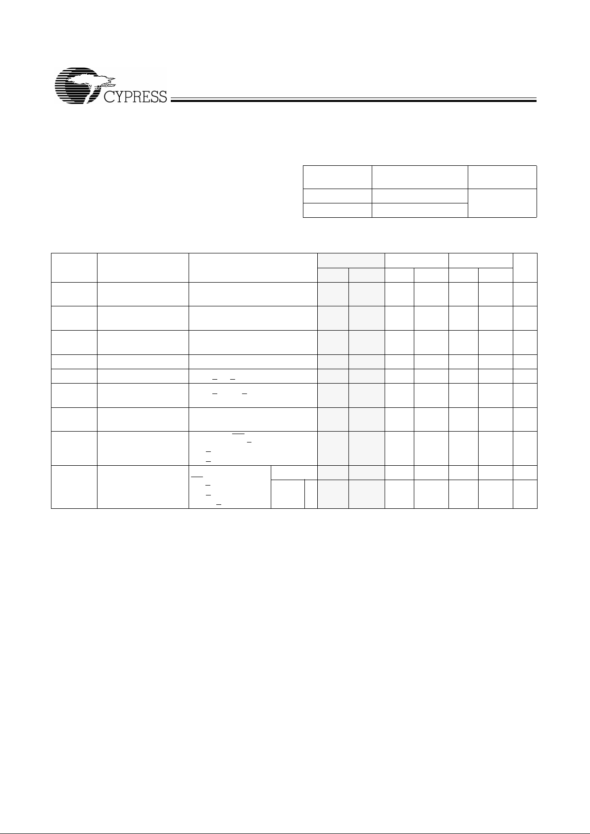
Selectio n Gu ide
1049V33-12 1049V33-15 1049V33-17 1049V33-20 1049V33-25
Maximum Access Time (ns) 12 15 17 20 25
Maximum Operating Current (mA) 150 140 130 120 110
Maximum CMOS Standby
Current (mA)
Com’l/Ind’l 8888 8
Com’l L 0.5 0.5 0.5 0.5 0.5
Shaded areas contain preliminary information.
CY7C1049V33
2
Maximum Ratings
(Above which the useful lif e m ay be impaired. For user guidelines, not tested.)
Storage Temperature ................... ........... .. .–65°C to +150°C
Ambient Temperature with
Power Applied.............................................–55°C to +125°C
Supply Voltage on VCC to Relative GND
[1]
....–0.5V to +4.6V
DC V oltage Applied to Outputs
in High Z State
[1]
....................................–0.5V to VCC + 0.5V
DC Input Voltage
[1]
................................–0.5V to VCC + 0.5V
Curre n t in to Out p ut s (L OW )........ ......... .......... .......... .... 20 mA
Operating Range
Range
Ambient
Temperature
[2]
V
CC
Commercial 0°C to +70°C 3.3V ± 0.3V
Industrial –40°C to +85°C
Electrical Characteristics
Over the Operating Range
Parameter Description Test Conditions
7C1049V33-12 7C1049V33-15 7C1049V33-17
Min. Max. Min. Max. Min. Max. Unit
V
OH
Output HIGH Voltage VCC = Min.,
I
OH
= –4.0 mA
2.4 2.4 2.4 V
V
OL
Outp u t LOW Voltage VCC = Min.,
I
OL
= 8.0 mA
0.4 0.4 0.4 V
V
IH
Input HIGH Voltage 2.2 V
CC
+ 0.5
2.2 V
CC
+ 0.5
2.2 V
CC
+ 0.5
V
V
IL
Input LOW Voltage
[1]
–0.5 0.8 –0.5 0.8 –0.5 0.8 V
I
IX
Input Load Current GND < VI < V
CC
–1 +1 –1+1–1+1µA
I
OZ
Output Leakage
Current
GND < V
OUT
< VCC,
Output Disabled
–1 +1 –1+1–1+1µA
I
CC
VCC Operating
Supply Current
VCC = Max.,
f = f
MAX
= 1/t
RC
150 140 130 mA
I
SB1
Automatic CE
Power-Down Current
—TTL Inputs
Max. VCC, CE > V
IH
VIN > VIH or
V
IN
< VIL, f = f
MAX
30 30 30 mA
I
SB2
Automatic CE
Power-Down Current
—CMOS Inputs
Max. VCC,
CE
> VCC – 0.3V,
V
IN
> VCC – 0.3V,
or V
IN
< 0.3V, f=0
Com’l/Ind’l
888mA
Com’lL
0.5 0.5 0.5 mA
Shaded areas contain preliminary information.
Notes:
1. V
IL
(min.) = –2.0V for pulse durations of less than 20 ns.
2. T
A
is the “Instant On” case temperature.
CY7C1049V33
3
Electrical Characteristics
Over the Operating Range (continued)
7C1049V33-20 7C1049V33-25
Parameter Description Test Conditions Min. Max. Min. Max. Unit
V
OH
Output HIGH Voltage VCC = Min.,
I
OH
= –4.0 mA
2.4 2.4 V
V
OL
Output LOW Voltage VCC = Min.,
I
OL
= 8.0 mA
0.4 0.4 V
V
IH
Input HIGH Voltage 2.2 V
CC
+ 0.5 2.2 VCC + 0.5 V
V
IL
Input LOW Voltage
[1]
–0.5 0.8 –0.5 0.8 V
I
IX
Input Load Current GND < VI < V
CC
–1+1–1+1µA
I
OZ
Output Leakage
Current
GND < V
OUT
< VCC,
Output Disabled
–1+1–1+1µA
I
CC
VCC Operating
Supply Current
VCC = Max.,
f = f
MAX
= 1/t
RC
120 110 mA
I
SB1
Autom a t i c C E
Po wer-Down Current
—TTL Inpu ts
Max. VCC, CE > V
IH
VIN > VIH or
V
IN
< VIL, f = f
MAX
30 30 mA
I
SB2
Autom a t i c C E
Po wer-Down Current
—CMOS Inputs
Max. V
CC
,
CE
> VCC – 0.3V,
V
IN
> VCC – 0.3V,
or V
IN
< 0.3V, f=0
Com’l/Ind’l8 8mA
Com’lL 0.5 0.5 mA
Capacitance
[3]
Parameter Description Te st Condi tions Max. Unit
C
IN
Input Capacitance TA = 25°C, f = 1 MHz,
V
CC
= 3.3V
8pF
C
OUT
I/O Capacitance 8 pF
Note:
3. Tested initially and after any design or process changes that may affect these parameters.
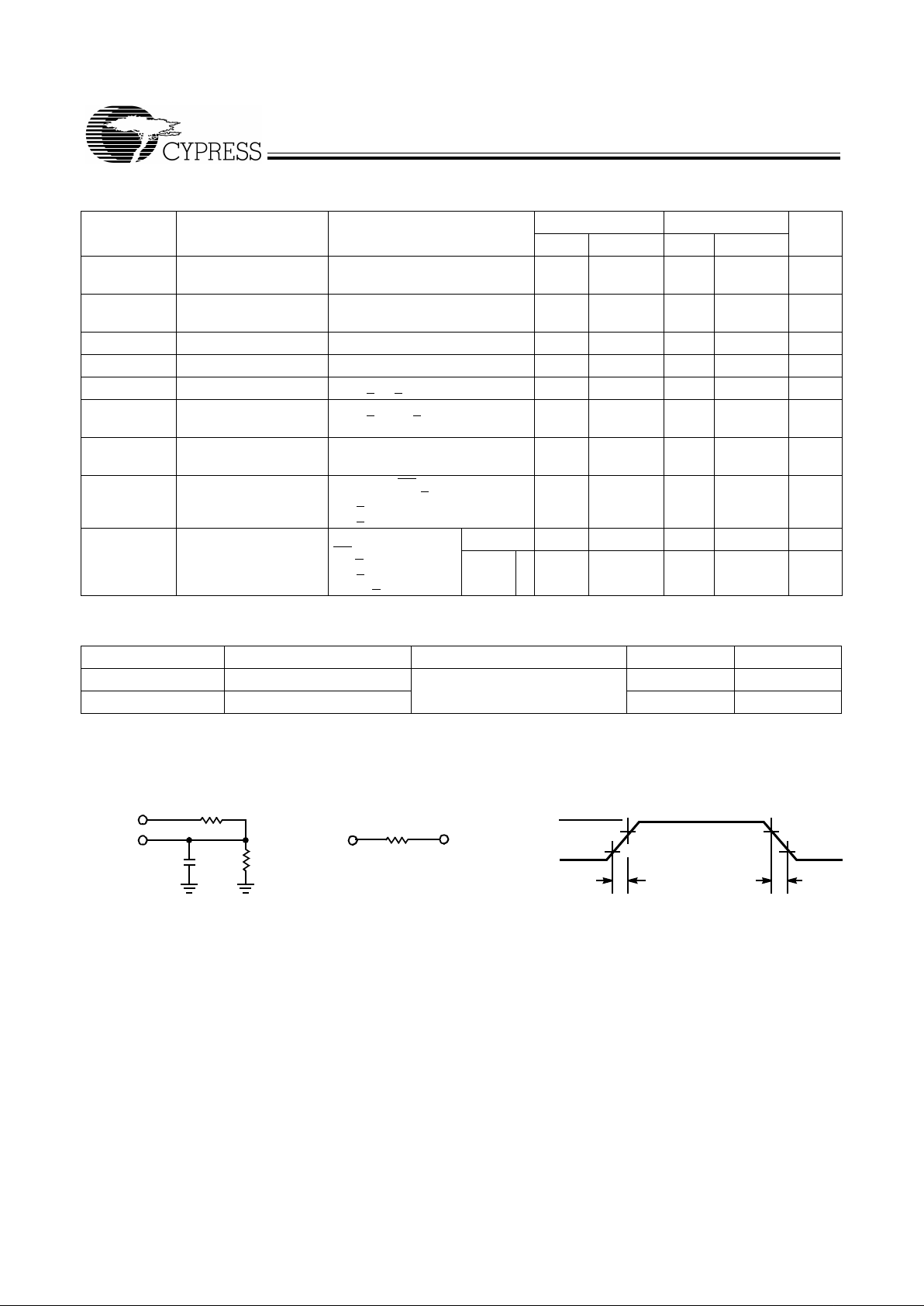
AC Test Loads and Waveforms
1049V33–3
1049V33–4
90%
10%
3.3V
GND
90%
10%
ALL INPUT PULSES
3.3V
OUTPUT
30 pF
INCLUDING
JIG AND
SCOPE
OUTPUT
(a)
(b)
≤
3 ns
≤
3ns
R1 317
Ω
167
Ω
R2
351
Ω
VENIN EQUIVALENT
THÉ
1.73V
 Loading...