

Cypress Semiconductor CY7C1049-20VI, CY7C1049-20VC, CY7C1049-17VC, CY7C1049-15VC, CY7C1049L-25VC Datasheet
...
049
PRELIMINARY
512K x 8 Static RAM
Features
• High speed
= 15 ns
—t
AA
• Low active pow er
—1210 mW (max.)
• Low CMOS standby power (Commercial L ver sion)
—2.75 mW (max.)
• 2.0V Data Retention (400 µW at 2.0V retention)
• Automatic power-down when deselected
• TTL-compatible inputs and outputs
• Easy memory expansion with CE
and OE f eatures
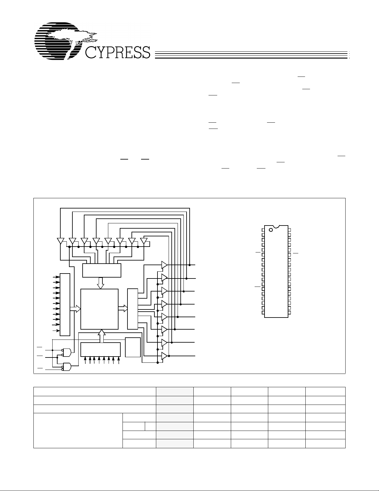
Functional Description
The CY7C1049 is a high-performance CMOS static RAM organized as 524,288 words by 8 bit s. Easy memory expansion
Logic Block Diagram Pin Configuration
is provided b y an activ e LOW chip enab le (CE
output enable (OE
), and three-stat e drivers. Writing t o the device is accomp lished by taki ng chip enable (CE
able (WE
I/O
pins (A
) inputs LO W . Data on the eight I/O pins ( I/O0 through
) is then written into the location specified on the address
7
through A18).
0
Reading from the device is accomplished by taking chip enable (CE
able (WE
) and output enabl e (OE) LOW while f or cing write en-
) HIGH. Under these conditions, the contents of the
memory location specified by the address pins will appear on
the I/O pins.
The eight input/output pins (I/O
high-impedance state when the device is deselected (CE
through I/O7) are placed in a
0
HIGH), the outputs are disabled (OE HIGH), or during a write
operation (CE
LOW, and WE LOW).
The CY7C1049 is available in a stan dard 400-mil-wide 36-pin
SOJ package with center power and ground (revolutionary)
pinout.
SOJ
Top View
CY7C1049
), an active LO W
) and write en-
WE
OE
A
0
A
1
A
2
A
3
A
4
CE
I/O
0
I/O
I/O
I/O
I/O
I/O
I/O
I/O
I/O
1049–1
0
1
2
3
4
5
6
7
INPUT BUFFER
A
0
A
1
A
2
A
3
A
4
A
5
A
6
A
7
A
A
A
ROW DECODER
8
9
10
512K x 8
ARRAY
COLUMN
DECODER
11
12
A
A13A
14
ACEA
SENSE AMPS
POWER
DOWN
15
16
17
18
A
A
A
I/O
V
GND
I/O
I/O3
WE
1
CC
2
A
5
A
6
A
7
A
8
A
9
36
1
2
3
4
5
6
7
8
9
10
11
12
13
14
15
16
17
18
NC
35
A
18
34
A
17
33
A
16
32
A
15
31
OE
30
I/O
7
29
I/O
6
28
GND
27
V
CC
26
I/O
5
25
I/O
4
24
A
14
23
A
13
22
A
12
21
A
11
20
A
10
19
NC
1049–2
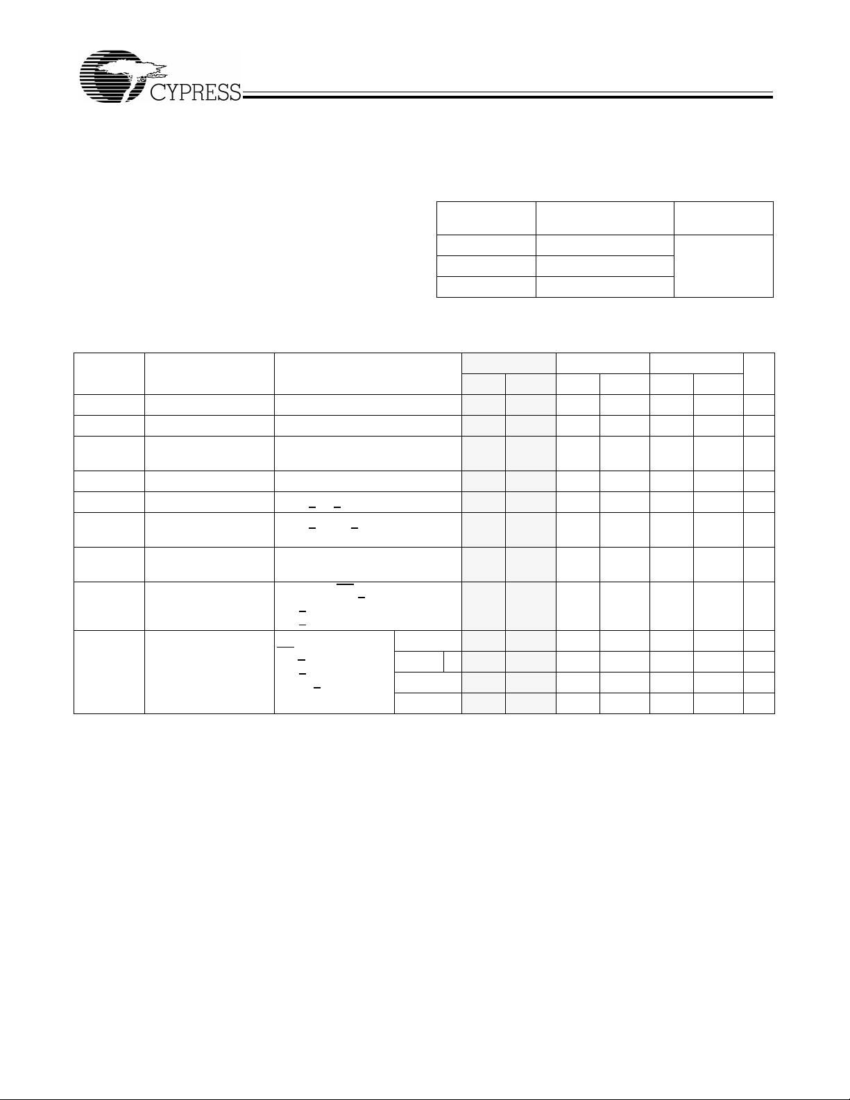
Selection G uide
7C1049-12 7C1049-15 7C1049-17 7C1049-20 7C1049-25
Maximum Access Time (ns) 12 15 17 20 25
Maximum Operat ing Current (mA) 240 220 195 185 180
Maximum CMOS Standby
Current (mA)
Shaded areas contain advance information.
Com’l 888 8 8
Com’l L 0.5 0.5 0.5 0.5 0.5
Ind’l 999 9 9
Military 10 10
Cypress Semiconductor Corporation
• 3901 North First Street • San Jose • CA 95134 • 408-943-2600
December 1996 – Re vised April 6, 1998
PRELIMINARY
Maximum Ratings
(Abov e which the useful life ma y be impaired. For user guidelines, not tested.)
Storage Temperature ...... ....... ... .. ........ .. .....–65°C to +1 5 0°C
Ambient Temperature with
Power Applied ............................................. –55°C to +12 5°C
Supply Voltage on VCC to Relative GND
DC Voltage Applied to Outputs
in High Z State
DC Input Voltage
[1]
....................................–0.5V to VCC + 0.5V
[1]
.................................–0.5V to VCC + 0.5V
Current into Outputs (LOW) .........................................20 mA
Electrical Characteristics
Parameter Description Test Conditions
V
OH
V
OL
V
IH
V
IL
I
IX
I
OZ
I
CC
I
SB1
I
SB2
Shaded areas contain advance information.
Notes:
1. V
2. T
A
Output HIGH V ol ta ge VCC = Min., IOH = –4.0 mA 2.4 2.4 2.4 V
Output LO W Voltage VCC = Min., IOL = 8.0 mA 0.4 0.4 0.4 V
Input HIGH Voltage 2.2 V
Input LOW Voltage
[1]
Input Load Current GND < VI < V
Output Leakage
Current
VCC Operating
Supply Current
Automatic CE
P ower-Down Current
—TTL Inputs
Automatic CE
P ower-Down Current
—CMOS Inputs
(min.) = –2.0V f or pulse durati ons o f les s than 2 0 ns.
IL
is the “i nstan t on” case temperature.
[1]
....–0.5V to +7.0V
Over the Operating Range
CC
GND < V
Output Disabled
VCC = Max.
f = f
MAX
Max. V
VIN > VIH or
V
< VIL, f = f
IN
OUT
= 1/t
, CE > V
CC
< VCC,
,
RC
IH
MAX
Max. VCC,
CE
> VCC – 0.3V,
V
> VCC – 0.3V,
IN
or V
< 0.3V, f=0
IN
Com’l
Com’lL
Ind’l
Military
CY7C1049
Static Discharge Voltage ............................ .. .............>2001V
(per MIL-STD-883, Method 3015)
Latch-Up Current.....................................................>200 mA
Operating Range
Ambient
Range
Temperature
Commercial 0°C to +70°C 4.5V–5.5V
Industrial –40°C to +85°C
Military –55°C to +125°C
7C1049-12 7C1049-15 7C1049-17
Min. Max. Min. Max. Min. Max. Unit
2.2 V
CC
+ 0.3
–0.3 0.8 –0.3 0.8 –0.3 0.3 V
–1 +1 –1+1–1+1µA
–1 +1 –1+1–1+1µA
240 220 195 mA
40 40 40 mA
888mA
0.5 0.5 0.5 mA
999mA
10 10 10 mA
CC
+ 0.3
[2]
2.2 V
V
CC
CC
+ 0.3
V
2
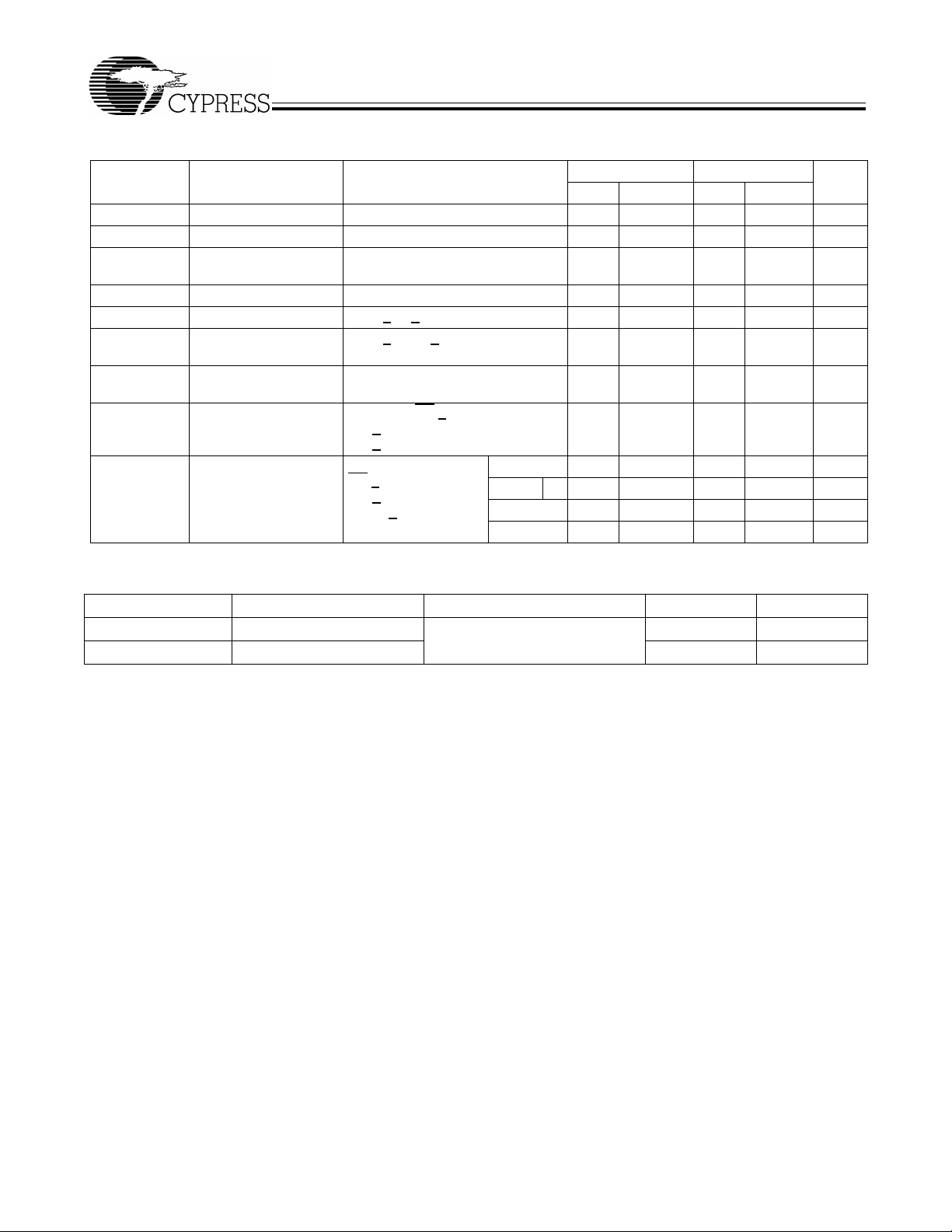
Electrical Characteristics
PRELIMINARY
Over the Op erating Range (continued)
CY7C1049
Test Conditions 7C1049-20 7C1049-25
Parameter Description Min. Max. Min. Max. Unit
V
V
V
V
I
IX
I
OZ
I
CC
I
SB1
I
SB2
OH
OL
IH
IL
Output HIGH Voltage VCC = Min., IOH = –4.0 mA 2.4 2.4 V
Output LOW Voltage VCC = Min., IOL = 8.0 mA 0.4 0.4 V
Input HIGH Voltage 2.2 V
+ 0.3
Input LOW Voltage
Input Load Current GND < VI < V
Output Leakage
Current
VCC Operating
Supp ly Cur r ent
Automatic CE
Power-Down Current
—TTL Inputs
Automatic CE
Power-Down Current
—CMOS Inputs
[1]
GND < V
Output Disabled
VCC = Max.
f = f
Max. V
VIN > VIH or
V
IN
Max. VCC,
CE
V
IN
or V
CC
< VCC,
OUT
,
= 1/t
MAX
< VIL, f = f
, CE > V
CC
RC
MAX
> VCC – 0.3V,
> VCC – 0.3V,
< 0.3V, f=0
IN
–0.3 0.8 –0.3 0.8 V
–1+1–1+1µA
–1+1–1+1µA
IH
Com’l88mA
Com’lL 0.5 0.5 mA
Ind’l99mA
CC
2.2 V
185 180 mA
40 40 mA
CC
0.3
+
Military 10 10 mA
V
Capacitance
[3]
Parameter Description T est Conditions Max. Unit
C
IN
C
OUT
Note:
3. Tested initially and after any design or process changes that may affect these parameters.
Input Capacitance TA = 25°C, f = 1 MHz,
V
= 5.0V
I/O Capacitance 8 pF
CC
8pF
3
 Loading...