

Datasheet CY7C1041BL-17ZC, CY7C1041BL-17VC, CY7C1041BL-15ZC, CY7C1041BL-15VC, CY7C1041B-25ZI Datasheet (Cypress Semiconductor)
...
1CY7C1041B
CY7C1041B
256K x 16 Static RAM
Features
written into the location specified on the address pins (A
through A17). If Byte High Enable (BHE) is LOW, then data
• High speed
—tAA = 12 ns
• Low active power
—1540 mW (max.)
• Low CMOS standby power (L version)
—2.75 mW (max.)
• 2.0V Data Retention (400 µW at 2.0V retention)
• Automatic power-down when deselected
• TTL-compatible inputs and outputs
• Easy memory expansion with CE
and OE features
Functional Description
The CY7C1041B is a high-perf ormance CMOS st atic RAM organized as 262,144 words by 16 bits.
Writing to the device is accomplished by taking Chip Enable
) and Write Enable (WE) inputs L OW. If Byte Low Enable
(CE
) is LOW, then data from I/O pins (I/O0 through I/O7), is
(BLE
from I/O pins (I/O8 through I/O15) is written into the location
specified on the address pins (A
through A17).
0
Reading fr om th e device is accom pli shed by tak ing Chip E nable (CE
Enable (WE
) and Output Enable (OE) LOW while forcing the Wri te
) HIGH. I f Byte Low Enable (BLE) is LOW, then
data from the memory location specified by the address pins
will appear on I/O
then data from memory will appear on I/O
to I/O7. If Byte High Enable (BHE) is LOW,
0
truth table at the bac k of this data sheet f or a complete description of read and write modes.
The input/output pins (I/O
high-impedance state when the device is deselected (CE
through I/O15) are placed in a
0
HIGH), the outputs are disab led (OE HIGH), the BHE and BLE
are disable d (BHE, BLE HIGH), or du ring a write operation (CE
LOW, and WE LOW).
The CY7C1041B is available in a standard 44-pin
400-mil-wide body width SOJ and 44-pin TSOP II package
with center power and ground (revolutionary) pinout.
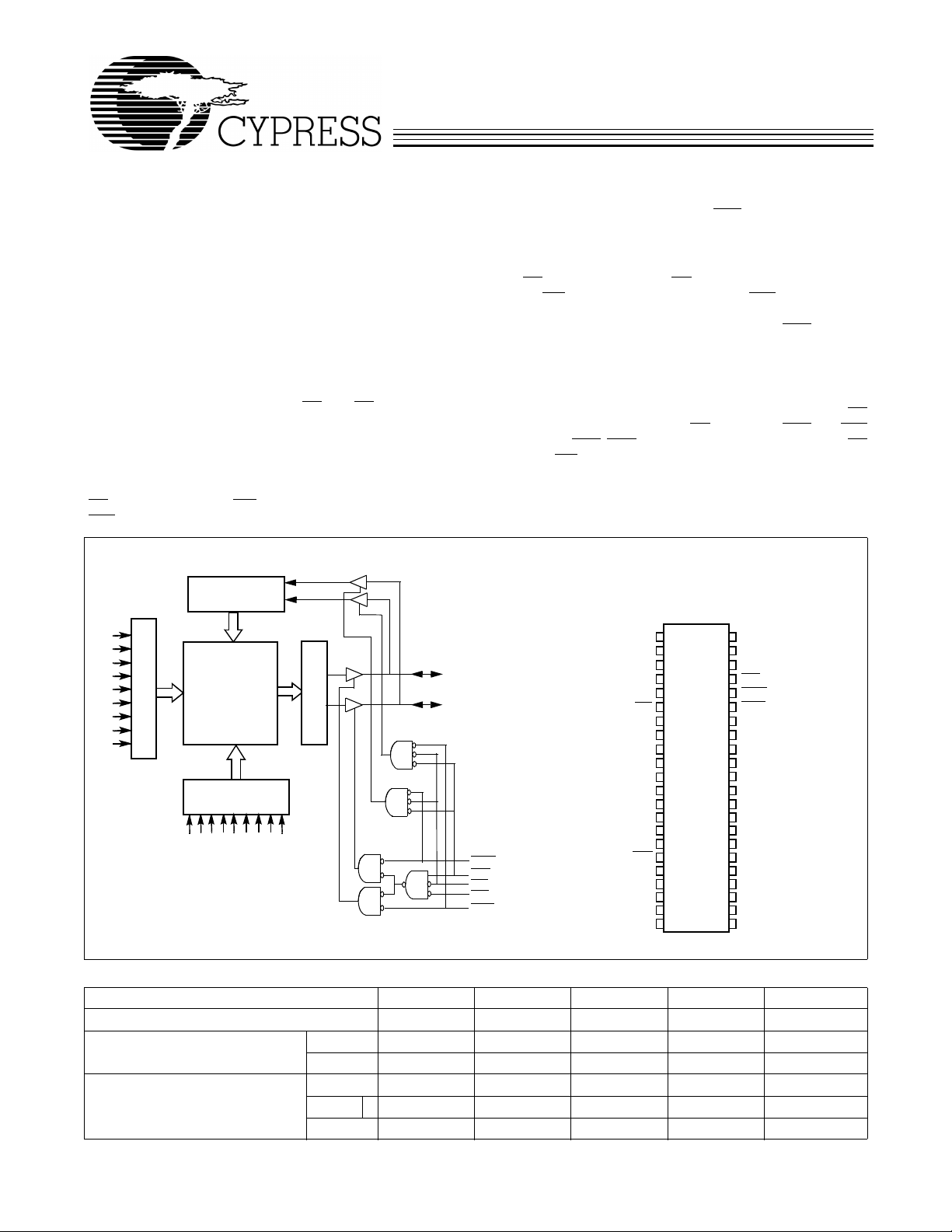
Logic Block Diagram Pin Configuration
A
A
A
A
A
CC
SS
A
A
A
A
A
0
1
2
3
4
0
1
2
3
4
5
6
7
5
6
7
8
9
SOJ
TSOP II
Top View
1
2
3
4
5
6
7
8
9
10
11
12
13
14
15
16
17
18
19
20
21
22
44
43
42
41
40
39
38
37
36
35
34
33
32
31
30
29
28
27
26
25
24
23
INPUT BUFFER
A
0
A
1
A
2
A
3
A
4
A
5
A
A
A
ROW DECODER
6
7
8
256K x 16
ARRAY
1024 x 4096
SENSE AMPS
I/O0 – I/O
I/O8 – I/O
7
15
CE
I/O
I/O
I/O
I/O
V
COLUMN
DECODER
V
I/O
I/O
11
14
15
12
A13A
AAA
16
17
A
BHE
WE
CE
OE
9
10
A
A
A
I/O
I/O
WE
BLE
1041B–1
to I/O15. See the
8
A
17
A
16
A
15
OE
BHE
BLE
I/O
15
I/O
14
I/O
13
I/O
12
V
SS
V
CC
I/O
11
I/O
10
I/O
9
I/O
8
NC
A
14
A
13
A
12
A
11
A
10
1041B–2
0
Selection Guide
7C1041B-12 7C1041B-15 7C1041B-17 7C1041B-20 7C1041B-25
Maximum Access Time (ns) 12 15 17 20 25
Maximum Operating Current (mA) Com’l 200 190 180 170 160
Ind’l 220 210 200 190 180
Maximum CMOS Standby Current
(mA)
Cypress Semiconductor Corporation • 3901 North First Street • San Jose • CA 95134 • 408-943-2600
Com’l 3 3 3 3 3
Com’l L- 0.5 0.5 0.5 0.5
Ind’l - 6 6 6 6
March 23, 2001
Maximum Ratings
(Above which the useful life may be impaired. For user guidelines, not tested.)
Storage Temperature –65°C to +150°C
Ambient Temperature with
Po wer Applied–55°C to +125°C
Supply Voltage on V
DC Voltage Applied to Outputs
in High Z State
[1]
to Relative GND
CC
–0.5V to VCC + 0.5V
[1]
–0.5V to +7.0V
CY7C1041B
[1]
DC Input Voltage
Current into Outputs (LOW)20 mA
Operating Range
Range
Commercial 0°C to +70°C 5V ± 0.5
Industrial –40°C to +85°C
–0.5V to VCC + 0.5V
Ambient
Temperature
[2]
V
CC
Electrical Characteristics
Over the Operating Range
Parameter Description Test Conditions
V
OH
V
OL
V
IH
V
IL
I
IX
I
OZ
I
CC
I
SB1
I
SB2
Notes:
1. V
2. T
A
Output HIGH Voltage VCC = Min., IOH = –4.0 mA 2.4 2.4 2.4 V
Output LOW Voltage VCC = Min., IOL = 8.0 mA 0.4 0.4 0.4 V
Input HIGH Voltage 2.2 V
Input LOW Voltage
Input Load Current GND < VI < V
Output Leakage
Current
VCC Operating
Supply Current
Automatic CE
Power-Down Current
—TTL Inputs
Automatic CE
Power-Down Current
—CMOS Inputs
(min.) = –2.0V for pulse dur ations of le ss than 20 ns.
IL
is the case temper atur e.
[1]
GND < V
Output Disabled
VCC = Max.,
f = f
MAX
Max. VCC, CE > V
VIN > VIH or
VIN < VIL, f = f
Max. V
CC
> VCC – 0.3V,
CE
> VCC – 0.3V,
V
IN
or VIN < 0.3V, f = 0
OUT
= 1/t
,
CC
< VCC,
RC
MAX
Com’l 200 190 180 mA
Ind’l 220 210 200 mA
IH
Com’l 3 3 3 mA
Com’l L - 0.5 0.5 mA
Ind’l - 6 6 mA
7C1041B-12 7C1041B-15 7C1041B-17
Min. Max. Min. Max. Min. Max. Unit
CC
+ 0.5
2.2 V
CC
+ 0.5
2.2 V
CC
+ 0.5
V
–0.5 0.8 –0.5 0.8 –0.5 0.8 V
–1 +1 –1 +1 –1 +1 µA
–1 +1 –1 +1 –1 +1 µA
40 40 40 mA
2
CY7C1041B
Electrical Characteristics
Over the Operating Range (continued)
Test Conditions 7C1041B-20 7C1041B-25
Parameter Description Min. Max. Min. Max. Unit
V
OH
V
OL
V
IH
V
IL
I
IX
I
OZ
I
CC
I
SB1
I
SB2
Capacitance
Output HIGH Voltage VCC = Min., IOH = –4.0 mA 2.4 2.4 V
Output LOW Voltage VCC = Min., IOL = 8.0 mA 0.4 0.4 V
Input HIGH Voltage 2.2 V
Input LOW Voltage
Input Load Current GND < VI < V
Output Leakage
Current
VCC Operating
Supply Current
Automatic CE
Power-Down Current
—TTL Inputs
Automatic CE
Power-Down Current
—CMOS Inputs
[3]
[1]
GND < V
Output Disabled
VCC = Max.,
f = f
MAX
Max. VCC, CE > V
VIN > VIH or
VIN < VIL, f = f
Max. VCC,
CE > VCC – 0.3V,
> VCC – 0.3V,
V
IN
or V
OUT
= 1/t
RC
< 0.3V, f = 0
IN
CC
< VCC,
MAX
–0.5 0.8 –0.5 0.8 V
–1 +1 –1 +1 µA
–1 +1 –1 +1 µA
Com’l 170 160 mA
Ind’l 190 180 mA
IH
Com’l 3 3 mA
Com’l L 0.5 0.5 mA
Ind’l 6 6 mA
CC
+ 0.5
40 40 mA
2.2 VCC + 0.5 V
Parameter Description Test Conditions Max. Unit
C
IN
C
OUT
Input Capacitance TA = 25°C, f = 1 MHz,
I/O Capacitance 8 pF
VCC = 5.0V
8pF
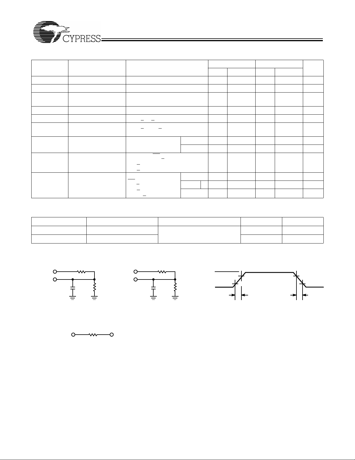
AC Test Loads and Waveforms
ALL INPUT PULSES
90%
10%
30 pF
R1 481Ω
(a)
THÉ
167Ω
R2
255Ω
5V
OUTPUT
INCLUDING
JIG AND
SCOPE
1.73V
5V
OUTPUT
INCLUDING
JIG AND
SCOPE
Equivalent to: VENIN EQUIVALENT
OUTPUT
Note:
3. Tested initially and after any design or process changes that may affect these parameters.
5 pF
R1 481Ω
(b)
R2
255Ω
1041B–3
3.0V
GND
≤ 3 ns ≤ 3
90%
10%
ns
1041B–4
3

CY7C1041B
Switching Characteristics
[4]
Over the Operating Range
7C1041B-12 7C1041B-15 7C1041B-17
Parameter Description M in. Max. Min. Max. Min. Max. Unit
READ CYCLE
t
power
t
RC
t
AA
t
OHA
t
ACE
t
DOE
t
LZOE
t
HZOE
t
LZCE
t
HZCE
t
PU
t
PD
t
DBE
t
LZBE
t
HZBE
WRITE CYCLE
t
WC
t
SCE
t
AW
t
HA
t
SA
t
PWE
t
SD
t
HD
t
LZWE
t
HZWE
t
BW
Notes:
4. Test conditions assume signal transition time of 3 ns or less, timing reference levels of 1.5V, input pulse levels of 0 to 3.0V, and output loading of the specified
I
OL/IOH
5. This part has a voltage regulator which steps down the voltage from 5V to 3.3V internally. t
is started.
6. t
HZOE
7. At any given temperature and voltage condition, t
8. The internal write time of the memory is defined by the overlap of CE
these signals can terminate the write. The i nput da ta set- up and ho ld t iming sh ould be ref e renced to the l eading e dge of the s ignal t hat te rminates t he write .
9. The minimum write cycle time for Write Cycle no. 3 (WE
VCC(typical) to the First Access
Read Cycle Time 12 15 17 ns
Address to Data Valid 12 15 17 ns
Data Hold from Address Change 3 3 3 ns
CE LOW to Data Valid 12 15 17 ns
OE LOW to Data Valid 6 7 7 ns
OE LOW to Low Z 0 0 0 ns
OE HIGH to High Z
CE LOW to Low Z
CE HIGH to High Z
[6, 7]
[7]
[6, 7]
CE LOW to Power-Up 0 0 0 ns
CE HIGH to Power-Down 12 15 17 ns
Byte Enable to Data Valid 6 7 7 ns
Byte Enable to Low Z 0 0 0 ns
Byte Disable to High Z 6 7 7 ns
[8, 9]
Write Cycle Time 12 15 17 ns
CE LOW to Write End 10 12 14 ns
Address Set-Up to Write End 10 12 14 ns
Address Hold from Write End 0 0 0 ns
Address Set-Up to Write Start 0 0 0 ns
WE Pulse Width 10 12 14 ns
Data Set-Up to Write End 7 8 8 ns
Data Hold from Write End 0 0 0 ns
WE HIGH to Low Z
WE LOW to High Z
[7]
[6, 7]
Byte Enable to End of Write 10 12 12 ns
and 30-pF load ca pacitanc e.
, t
HZCE
, and t
are specified with a loa d capaci tance of 5 pF as in part (b) of A C Test Loads. Transition is measured ±500 mV from steady-state voltage .
HZWE
[5]
is less than t
HZCE
controlled, OE LOW) is the sum of t
, t
LZCE
HZOE
LOW , and WE LO W . CE and WE m ust be L O W to initia te a writ e, and t he trans ition of ei ther of
111ms
677ns
333ns
677ns
333ns
677ns
time has to be provided initially before a read/write operation
power
is less than t
LZOE
, and t
HZWE
is less than t
HZWE
and tSD.
for any giv en device.
LZWE
4

CY7C1041B
Switching Characteristics
[4]
Over the Operating Range (continued)
Parameter Description
READ CYCLE
t
power
t
RC
t
AA
t
OHA
t
ACE
t
DOE
t
LZOE
t
HZOE
t
LZCE
t
HZCE
t
PU
t
PD
t
DBE
t
LZBE
t
HZBE
WRITE CYCLE
t
WC
t
SCE
t
AW
t
HA
t
SA
t
PWE
t
SD
t
HD
t
LZWE
t
HZWE
t
BW
VCC(typical) to the First Access
Read Cycle Time 20 25 ns
Address to Data Valid 20 25 ns
Data Hold from Address Change 3 5 ns
CE LOW to Data Valid 20 25 ns
OE LOW to Data Valid 8 10 ns
OE LOW to Low Z 0 0 ns
OE HIGH to High Z
CE LOW to Low Z
CE HIGH to High Z
[6, 7]
[7]
[6, 7]
CE LOW to Power-Up 0 0 ns
CE HIGH to Power- Do wn 20 25 ns
Byte Enable to Data Valid 8 10 ns
Byte Enable to Low Z 0 0 ns
Byte Disable to High Z 8 10 ns
[8, 9]
Write Cycle Time 20 25 ns
CE LOW to Write End 13 15 ns
Address Set-Up to Write End 13 15 ns
Address Hold from Write End 0 0 ns
Address Set-Up to Write Start 0 0 ns
WE Pulse Width 13 15 ns
Data Set-Up to Write End 9 10 ns
Data Hold from Write End 0 0 ns
WE HIGH to Low Z
WE LOW to High Z
[7]
[6, 7]
Byte Enable to End of Write 13 15 ns
[5]
7C1041B-20 7C1041B-25
UnitMin. Max. Min. Max.
111
810ns
35ns
810ns
35ns
810ns
Data Retention Characteristics
Over the Operating Range (L versio n only )
Parameter Description Conditions
V
DR
I
CCDR
[3]
t
CDR
[10]
t
R
Notes:
< 3 ns for the -12 and -15 s peeds. tr < 5 ns for the -2 0 and s low er s peeds.
10. t
r
11. No input may exceed V
VCC for Data Retention 2.0 V
Data Retention Current Com’l L VCC = VDR = 3.0V ,
> VCC – 0.3V,
Chip Deselect to Data Retention Time 0 ns
CE
> VCC – 0.3V or VIN < 0.3V
V
IN
Operation Recovery Time t
+ 0.5V.
CC
5
[11]
Min. Max. Unit
200 µA
RC
ns

Data Retention Waveform
V
CC
CE
Switching Waveforms
t
CDR
CY7C1041B
DATA RETENTION MODE
VDR> 2V
3.0V3.0V
t
R
1041B–5
Read Cycle No. 1
[12, 13]
ADDRESS
DATA OUT
PREVIOUS DATA VALID DATA VALID
Read Cycle No. 2 (OEControlled)
ADDRESS
CE
OE
BHE, BLE
DATA OUT
V
CC
SUPPLY
CURRENT
HIGH IMPEDANCE
t
LZCE
t
PU
[13, 14]
t
ACE
t
t
DBE
t
LZBE
t
t
DOE
LZOE
50%
OHA
t
RC
t
AA
1041B-6
t
RC
t
HZOE
t
HZCE
t
DATA VALID
HZBE
t
PD
HIGH
IMPEDANCE
ICC
50%
ISB
1041B-7
Notes:
12. Device is continuously selected. OE
is HIGH f or read cycle .
13. WE
14. Address valid prior to or coincident with CE tran sition LO W.
, CE, BHE, and/or BH E = VIL.
6

CY7C1041B
Switching Waveforms
Write Cycle No. 1 (CE
ADDRESS
CE
WE
BHE, BLE
DATAI/O
Controlled)
(continued)
[15, 16]
t
SA
t
AW
t
WC
t
SCE
t
PWE
t
BW
t
HA
t
SD
t
HD
1041B-8
Write Cycle No. 2 (BLEorBHE Controlled)
ADDRESS
t
,BLE
BHE
WE
CE
DATAI/O
Notes:
15. Data I/O is high impedance if OE
16. If CE
goes HIGH simultaneous ly with WE going HIGH , the out put re mains in a hi gh-imp edance st ate .
SA
or BHE and/or BLE= VIH.
t
AW
t
WC
t
BW
t
t
PWE
SCE
t
HA
t
SD
t
HD
1041B-9
7

CY7C1041B
Switching Waveforms
(continued)
Write Cycle No. 3 (WE Controlled, LOW)OE
ADDRESS
CE
t
SA
WE
BHE
, BLE
DATA I/O
t
WC
t
SCE
t
AW
t
BW
t
HZWE
t
PWE
t
SD
t
HA
t
HD
t
LZWE
1041B-10
Truth Table
CE OE WE BLE BHE I/O0–I/O
7
H X X X X High Z High Z Power Down Standby (ISB)
L L H L L Data Out Data Out Read All bits Active (ICC)
L L H L H Data Out High Z Read Lower bits only Active (ICC)
L L H H L High Z Data Out Read Upper bits only Active (ICC)
L X L L L Data In Data In Write All bits Active (ICC)
L X L L H Data In High Z Writ e Lower bits only Active (ICC)
L X L H L High Z Data In Write Upper bits only Active (ICC)
L H H X X High Z High Z Selected, Outputs Disabled Active (ICC)
I/O8–I/O
15
Mode Power
8

Ordering Information
CY7C1041B
Speed
(ns) Ordering Code
12 CY7C1041B-12VC V34 44-Lead (400-Mil) Molded SOJ Commercial
CY7C1041B-12ZC Z44 44-Lead TSOP Type II
15 CY7C1041B-15VC V34 44-Lead (400-Mil) Molded SOJ
CY7C1041BL-15VC V34 44-Lead (400-Mil) Molded SOJ
CY7C1041B-15ZC Z44 44-Lead TSOP Type II
CY7C1041BL-15ZC Z44 44-Lead TSOP Type II
17 CY7C1041B-17VC V34 44-Lead (400-Mil) Molded SOJ
CY7C1041BL-17VC V34 44-Lead (400-Mil) Molded SOJ
CY7C1041B-17ZC Z44 44-Lead TSOP Type II
CY7C1041BL-17ZC Z44 44-Lead TSOP Type II
20 CY7C1041B-20VC V34 44-Lead (400-Mil) Molded SOJ
CY7C1041BL-20VC V34 44-Lead (400-Mil) Molded SOJ
CY7C1041B-20ZC Z44 44-Lead TSOP Type II
CY7C1041BL-20ZC Z44 44-Lead TSOP Type II
25 CY7C1041B-25VC V34 44-Lead (400-Mil) Molded SOJ
CY7C1041BL-25VC V34 44-Lead (400-Mil) Molded SOJ
CY7C1041B-25ZC Z44 44-Lead TSOP Type II
CY7C1041BL-25ZC Z44 44-Lead TSOP Type II
15 CY7C1041B-15ZI Z44 44-Lead TSOP Type II Industrial
CY7C1041B-15VI V34 44-Lead (400-Mil) Molded SOJ
17 CY7C1041B-17ZI V34 44-Lead TSOP Type II
CY7C1041B-17VI Z44 44-Lead (400-Mil) Molded SOJ
20 CY7C1041B-20ZI Z44 44-Lead TSOP Type II
CY7C1041B-20VI Z44 44-Lead (400-Mil) Molded SOJ
25 CY7C1041B-25ZI Z44 44-Lead TSOP Type II
CY7C1041B-25VI Z44 44-Lead (400-Mil) Molded SOJ
Package
Name Package Type
Operating
Range
Document #: 38-00938-*B
9

Package Diagrams
CY7C1041B
44-Lead (400-Mil) Mo lded SOJ V3 4
44-Pin TSOP II Z44
51-85082-B
51-85087-A
© Cypress Semiconductor Corporation, 2001. The information contained herein is subject to change without notice. Cypress Semiconductor Corporation assumes no responsibility for the use
of any circuitry other than circui try embodied in a Cypress S emiconductor p roduct. Nor does it conv ey or imply an y license under pa tent or other rights. Cypre ss Semiconductor doe s not authorize
its products for use as critical components in life-support systems where a malfunction or failure may reasonably be expected to result in significant injury to the user. The inclusion of Cypress
Semiconductor products in life-support systems application implies that the manufacturer assumes all risk of such use and in doing so indemnifies Cypress Semiconductor against all charges.
 Loading...