

Datasheet CY7C1024AV33-15BGI, CY7C1024AV33-15BGC, CY7C1024AV33-15AC, CY7C1024AV33-12BGI, CY7C1024AV33-12BGC Datasheet (Cypress Semiconductor)
...
PRELIMINARY
32K x 16 Static RAM
CY7C1022
Cypress Semiconductor Corporation • 3901 North First Street • San Jose • CA 95134 • 408-943-2600
Document #: 38-05090 Rev. ** Revised September 18, 2001
022CY7C10
Features
• 5.0V operation (± 10%)
• High speed
—t
AA
= 12 ns
• Low active power
—825 mW (max., 10 ns, “L” version)
• Very Low stan dby pow er
—500 µW (max., “L” version)
• Automatic power-down when deselected
• Independent Control of Upper and Lower bytes
• Available in 400-mil SOJ
Functional Description
The CY7C1022 is a high-performance CMOS static RAM organized as 32,768 word s by 16 bits . Thi s de vi ce has an au tomatic power-down feature that significantly reduces power
consumption when deselected.
Writing to the device is accomplished by taking chip enable
(CE) input HIGH and write enable (WE
) input LOW . If byte low
enable (BLE
) is LOW, then data from I/O pins (I/O1 through
I/O
8
), is written into the locat ion spe ci fie d on th e ad dress pins
(A
0
through A14). If byte high en abl e (BH E) i s LO W, then da ta
from I/O pins (I/O
9
through I/O16) is written into the location
specified on the address pins (A
0
through A14).
Reading from the device is accomplished by taking chip enable (CE) HIGH and output enable (OE
) LOW while forcing the
write enable (WE) HIGH . If byte low enable (BLE) is LOW , then
data from the memory location specified by the address pins
will appear on I/O
1
to I/O8. If byte high enable (BHE) is LOW,
then data from memory will appear on I/O9 to I/O16. See the
truth table at the back of th is data sheet for a com plete description of read and write modes.
The input/output pins (I/O
1
through I/O16) are placed in a
high-impedance state when the device is deselected (CE
LOW), the outputs are dis abled (OE
HIGH), the BHE and BLE
are disabled (BHE, BLE HIGH), or during a write operation (CE
HIGH, and WE
LOW).
The CY7C1022 is available in standard 400-mil-wide SOJ
packages.
2CY7C1022
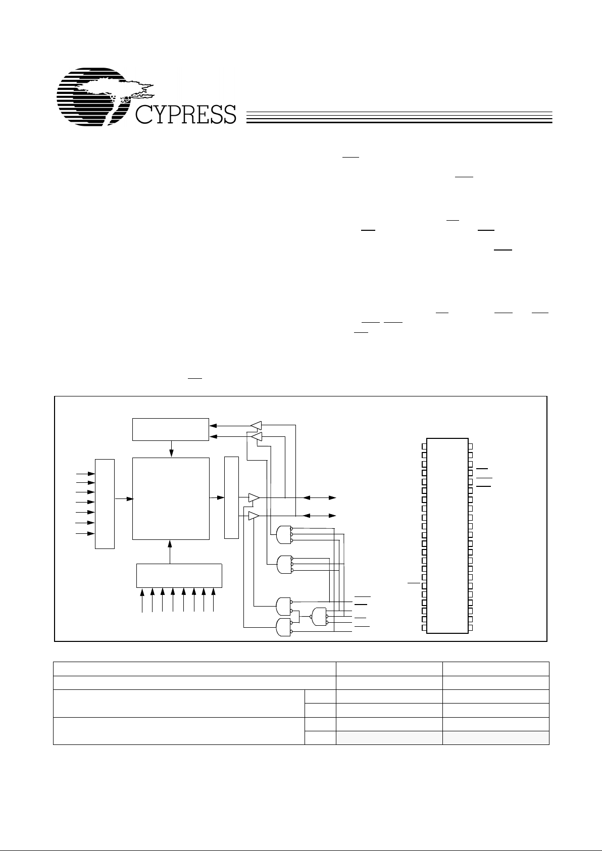
WE
Logic Block Diagram
Pin Configuration
1
2
3
4
5
6
7
8
9
10
11
14
31
32
36
35
34
33
37
40
39
38
Top View
SOJ
12
13
41
44
43
42
16
15
29
30
V
CC
A
10
A
9
A
8
A
7
NC
NC
A
14
OE
V
SS
A
0
I/O
16
A
13
I/O
3
I/O
1
I/O
2
BHE
NC
A
12
A
11
1022-2
18
17
20
19
I/O
4
27
28
25
26
22
21
23
24
NC
V
SS
I/O
7
I/O
5
I/O
6
I/O
8
A
1
A
2
BLE
V
CC
I/O
15
I/O
14
I/O
13
I/O
12
I/O
11
I/O
10
I/O
9
A
3
A
4
A
5
A
6
32K x 16
RAM Array
I/O
1
– I/O
8
ROW DECODER
A
6
A
5
A
4
A
3
A
0
COLUMN DECODER
A
9
A10A11A
12
A13A
14
SENSE AMPS
DATA IN DRIVERS
OE
A
2
A
1
I/O9 – I/O
16
CE
WE
BLE
BHE
A
8
A
7
CE
Selection Guide
7C1022-12 7C1022-15
Maximum Access Time (ns) 12 15
Maximum Operating Current (mA) 170 160
L 140 130
Maximum CMOS Standby Current (mA) 3 3
L 0.1 0.1
Shaded areas contain advance information.
CY7C1022
PRELIMINARY
Document #: 38-05090 Rev. ** Page 2 of 8
Maximum Ratings
(Above which the useful life may be im pai red. For user guidelines, not tested.)
Storage Temperature ................................–65×C to +150×C
Ambient Temperature with
Power Applied............................................–55×C to +125×C
Supply Voltage on V
CC
to Relative GND
[1]
....–0.5V to +7.0V
DC Voltage Applied to Outputs
in High Z State
[1]
....................................–0.5V to VCC + 0.5V
DC Input Voltage
[1]
................................–0.5V to VCC + 0.5V
Current into Outputs (LOW)........................................20 mA
Operating Range
Range
Ambient
Temperature
[2]
V
CC
Commercial 0°C to +70°C 4.5V–5.5V
Electrical Characteristics Ov er the Op erat ing Ran ge
Parameter Description Test Conditions
7C1022-12 7C1022-15
UnitMin. Max. Min. Max.
V
OH
Output HIGH Voltage VCC = Min., IOH = –4.0 mA 2.4 2.4 V
V
OL
Output LOW Vo ltage VCC = Min., IOL = 8.0 mA 0.4 0.4 V
V
IH
Input HIGH Voltage 2.2 6.0 2.2 6.0 V
V
IL
Input LOW Voltage
[1]
–0.5 0.8 –0.5 0.8 V
I
IX
Input Load Current GND < VI < V
CC
–1 +1 –1 +1 µA
I
OZ
Output Leakage
Current
GND < VI < VCC,
Output Disabled
–2 +2 –2 +2 µA
I
CC
VCC Operating
Supply Current
VCC = Max.
,
I
OUT
= 0 mA,
f = f
MAX
= 1/t
RC
170 160 mA
L 140 130
I
SB1
Automatic CE
Power-Down Current
—TTL Inputs
Max. VCC, CE > V
IH
VIN > VIH or
VIN < VIL, f = f
MAX
20 20 mA
L 10 10
I
SB2
Automatic CE
Power-Down Current
—CMOS Inputs
Max. VCC,
CE >
VCC – 0.3V,
V
IN
> VCC – 0.3V,
or VIN < 0.3V, f=0
3 3 mA
L 0.1 0.1 mA
Shaded area contains advance information.
Capacitance
[3]
Parameter Description Test Conditions Max. Unit
C
IN
Input Capacitance TA = 25°C, f = 1 MHz,
VCC = 5.0V
8 pF
C
OUT
Output Capacitance 8 pF
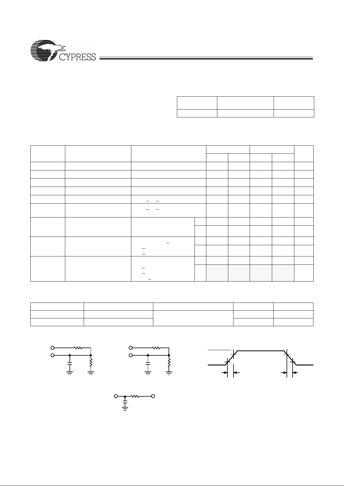
AC Test Loads and Waveforms
Notes:
1. V
IL
(min.) = –2.0V for pulse durations of less than 20 ns.
2. T
A
is the “instant on” case temp erature.
3. Tested initially and after any design or process changes that may affect these parameters.
1022-3
1022-4
90%
10%
3.0V
GND
90%
10%
ALL INPUT PULSES
5V
OUTPUT
30 pF
INCLUDING
JIG AND
SCOPE
5V
OUTPUT
5 pF
INCLUDING
JIG AND
SCOPE
(a)
(b)
<3ns <3ns
OUTPUT
R 481
Ω
R 481Ω
R2
255
Ω
R2
255
Ω
167Ω
Equivalent to:
THÉVENIN
EQUIVALENT
1.73V
30 pF
CY7C1022
PRELIMINARY
Document #: 38-05090 Rev. ** Page 3 of 8
Switching Characteristics
[4]
Over the Operating Range
Parameter Description
7C1022-12 7C1022-15
UnitMin. Max. Min. Max.
READ CYCLE
t
RC
Read Cycle Tim e 12 15 ns
t
AA
Address to Data V a lid 12 15 ns
t
OHA
Data Hold from Address Change 3 3 ns
t
ACE
CE HIGH to D ata Valid 12 15 ns
t
DOE
OE LOW to Data Valid 6 7 ns
t
LZOE
OE LOW to Low Z 0 0 ns
t
HZOE
OE HIGH to High Z
[5, 6]
6 7 ns
t
LZCE
CE HIGH to Low Z
[6]
3 3 ns
t
HZCE
CE LOW to High Z
[5, 6]
6 7 ns
t
PU
CE HIGH to Power-Up 0 0 ns
t
PD
CE LOW to Power-Down 12 15 ns
t
DBE
Byte enable to Data Valid 6 7 ns
t
LZBE
Byte enable to Low Z 0 0 ns
t
HZBE
Byte disable to High Z 6 7 ns
WRITE CYCLE
[7]
t
WC
Write Cycle Time 12 15 ns
t
SCE
CE HIGH to Write End 9 10 ns
t
AW
Address Set-Up to Write End 8 10 ns
t
HA
Address Hold from Write End 0 0 ns
t
SA
Address Set-Up to Write Start 0 0 ns
t
PWE
WE Pulse Width 8 10 ns
t
SD
Data Set-Up to Write End 6 10 ns
t
HD
Data Hold from Write End 0 0 ns
t
LZWE
WE HIGH to Low Z
[6]
3 3 ns
t
HZWE
WE LOW to High Z
[5, 6]
6 7 ns
t
BW
Byte enable to end of write 8 9 ns
Notes:
4. Test conditions assume signal transition time of 3 ns or less, timing reference levels of 1.5V, input pulse levels of 0 to 3.0V, and output loading of the specified
I
OL/IOH
and 30-pF load c apacitan ce.
5. t
HZOE
, t
HZBE
, t
HZCE
, and t
HZWE
are specified w ith a load ca pacitanc e of 5 pF as in part (b ) of AC Test Loads . T ran sition is m easured ±500 mV from steady-state voltag e.
6. At any given temperature and voltage condition, t
HZCE
is less than t
LZCE
, t
HZOE
is less than t
LZOE
, and t
HZWE
is less than t
LZWE
for any given dev ice.
7. The internal write time of the memory is defined by the overlap of CE HIG H, WE
LOW and BHE / BLE LOW. CE HIGH, WE and BHE / BLE must be LOW to initia te
a write, and the tra nsition of these si gnals can t erminate the write. The input data set-up an d hold ti ming should be referen ced to the leading edge of the s ignal that terminates
the write.

CY7C1022
PRELIMINARY
Document #: 38-05090 Rev. ** Page 4 of 8
Switching Waveforms
Notes:
8. Device is continuously selected. OE
, CE, BHE and/or BHE = V
IL
9. WE is HIGH for read cycle .
10. Address valid prior to or coinci dent with CE transition HIGH.
Read Cycle No.1
PREVIOUS DATA VALID DATA VALID
t
RC
t
AA
t
OHA
1022-5
ADDRESS
DATA OUT
[8, 9]
Read Cycle No.2 (OE Controlled)
1022-6
50%
50%
DATA VALID
t
ACE
t
DOE
t
LZOE
t
LZCE
t
PU
HIGH IMPEDANCE
t
HZOE
t
HZBE
t
PD
HIGH
OE
ICC
ISB
IMPEDANCE
ADDRESS
DATA OUT
V
CC
SUPPLY
t
DBE
t
LZBE
t
HZCE
BHE, BLE
[9, 10]
CURRENT
I
CC
I
SB
t
RC
CE

CY7C1022
PRELIMINARY
Document #: 38-05090 Rev. ** Page 5 of 8
Notes:
11. Data I/O is high impedance if OE
or BHE and/or BLE= VIH.
12. If CE goes LOW simult aneousl y wit h WE
going HIGH, the out put rema ins in a hi gh-impedanc e sta te.
Switching Waveforms (continued)
Write Cycle No. 1 (CE Controlled)
1022-7
t
HD
t
SD
t
SCE
t
SA
t
HA
t
AW
t
PWE
t
WC
BW
DATAI/O
ADDRESS
CE
WE
BHE, BLE
[11, 12]
t
Write Cycle No. 2 (BLEorBHE Controlled)
t
HD
t
SD
t
BW
t
SA
t
HA
t
AW
t
PWE
t
WC
t
SCE
DATAI/O
ADDRESS
BHE
,BLE
WE
CE
1022-8

CY7C1022
PRELIMINARY
Document #: 38-05090 Rev. ** Page 6 of 8
Switching Waveforms (continued)
Write Cycle No.3
(WE
Controlled, OE LOW)
1022-10
t
HD
t
SD
t
SCE
t
HA
t
AW
t
PWE
t
WC
t
BW
DATA I/O
ADDRESS
CE
WE
BHE
, BLE
t
SA
t
LZWE
t
HZWE
Tr uth Table
CE OE WE BLE BHE I/O1 - I/O
8
I/O9 - I/O
16
Mode Power
L X X X X High Z High Z Power-Down Standby (ISB)
H L H L L Data Out Data Out Read - All bits Active (ICC)
L H Data Out High Z Read - Lower bits only Active (ICC)
H L High Z Data Out Read - Upper bits only Active (ICC)
H X L L L Data In Data In Write - All b its Active (ICC)
L H Data In High Z Write - Lower bits only Active (ICC)
H L High Z Data In Write - Upper bits only Active (ICC)
H H H X X High Z High Z Selected, Outputs Disable d Active (ICC)
H X X H H High Z High Z Selected, Outputs Disabled Active (ICC)
Ordering Information
Speed
(ns) Ordering Code
Package
Name Package Type
Operating
Range
12 CY7C1022-12VC V34 44-Lead (400-Mil) Molded SOJ Commercial

CY7C1022
PRELIMINARY
Document #: 38-05090 Rev. ** Page 7 of 8
© Cypress Semiconductor Corporation, 2001. The information contained herein is subject to change without notice. Cypress Semiconductor Corporation assumes no responsibility for the use
of any circuitry other than circuitry embodied in a Cypress Semiconductor product. Nor does it convey or imply any license under patent or other rights. Cypress Semiconductor does not autho rize
its products for use as critical components in life-support systems where a malfunction or failure may reasonably be expected to result in significant injury to the user. The inclusion of Cypress
Semiconductor products in life-support systems application implies that the manufacturer assume s all risk of such use and in doi
ng so indemnifies Cypress Semiconductor against all charges.
Package Diagram
44-Lead (400-Mil) Molded SOJ V34

CY7C1022
PRELIMINARY
Document #: 38-05090 Rev. ** Page 8 of 8
Document Title: CY7C1022 32k x 16 Static RAM Data Sheet
Document Number: 38-05090
REV. ECN NO.
Issue
Date
Orig. of
Change Description of Change
** 110184 09/29/01 SZV Change from Spec number: 38-00636 to 38-05090
 Loading...