

Datasheet CY7C1021BV33L-15BAC, CY7C1021BV33L-12ZC, CY7C1021BV33L-12VC, CY7C1021BV33L-10ZC, CY7C1021BV33L-10VC Datasheet (Cypress Semiconductor)
...
021BV33
Features
• 3.3V operation (3.0V–3.6V)
• High speed
—t
= 10/12/15 ns
AA
• CMOS for optimum speed/power
• Low Active Power (L version)
—576 mW (max.)
• Low CMOS Standby Power (L version)
—1.80 mW (max.)
• Automatic power-down when deselected
• Independent control of upper and lower bits
• Available in 44-pin TSOP II and 400-mil SOJ
• Available in a 48-Ball Mini BGA package
Functional Description
The CY7C1021BV is a high-performance CMOS static RAM
organized as 65,5 36 wo rds by 16 b its. This device has an a utomatic power-down feature that significantly reduces power
consumption when deselected.
[1]
CY7C1021BV33
64K x 16 Static RAM
Writing to the device is accomplished by taking Chip Enable
) and Write Enable (WE) inputs LOW. If Byte Low Enable
(CE
) is LOW, then data from I/O pins (I/O1 through I/O8), is
(BLE
written into the location specified on the address pins (A
through A15). If Byte High Enable (BHE) is LOW, then data
from I/O pins (I/O
specified on the address pins (A
Reading from the device is accomplished by taking Chip Enable (CE
) and Output Enable (OE) LOW while f orcing the Write
Enable (WE
data from the memory location specified by the address pins
will appear on I/O
then data from memory will appear on I/O
truth table at the back of this data sheet for a complete description of read and write modes.
The input/output pins (I/O
high-impedance state when the device is deselected
HIGH), the outputs are disabled (OE HIGH), the BHE and
(CE
are disabled (BHE, BLE HIGH), or d uri ng a wri te o pera -
BLE
tion (CE
LOW, and WE LOW).
The CY7C1021BV is ava ilable in 400-mil-wide SOJ, st a nda rd
44-pin TSOP Type II, and 48-ball mini BGA packages.
through I/O
9
) is written into the location
16
through A
0
).
15
) HIGH. If Byte Low Enable (BLE) is LOW, then
to I/O
1
. If Byte High Enable (BHE) is L OW,
8
through I/O
1
to I/O16. See the
9
) are placed in a
16
0
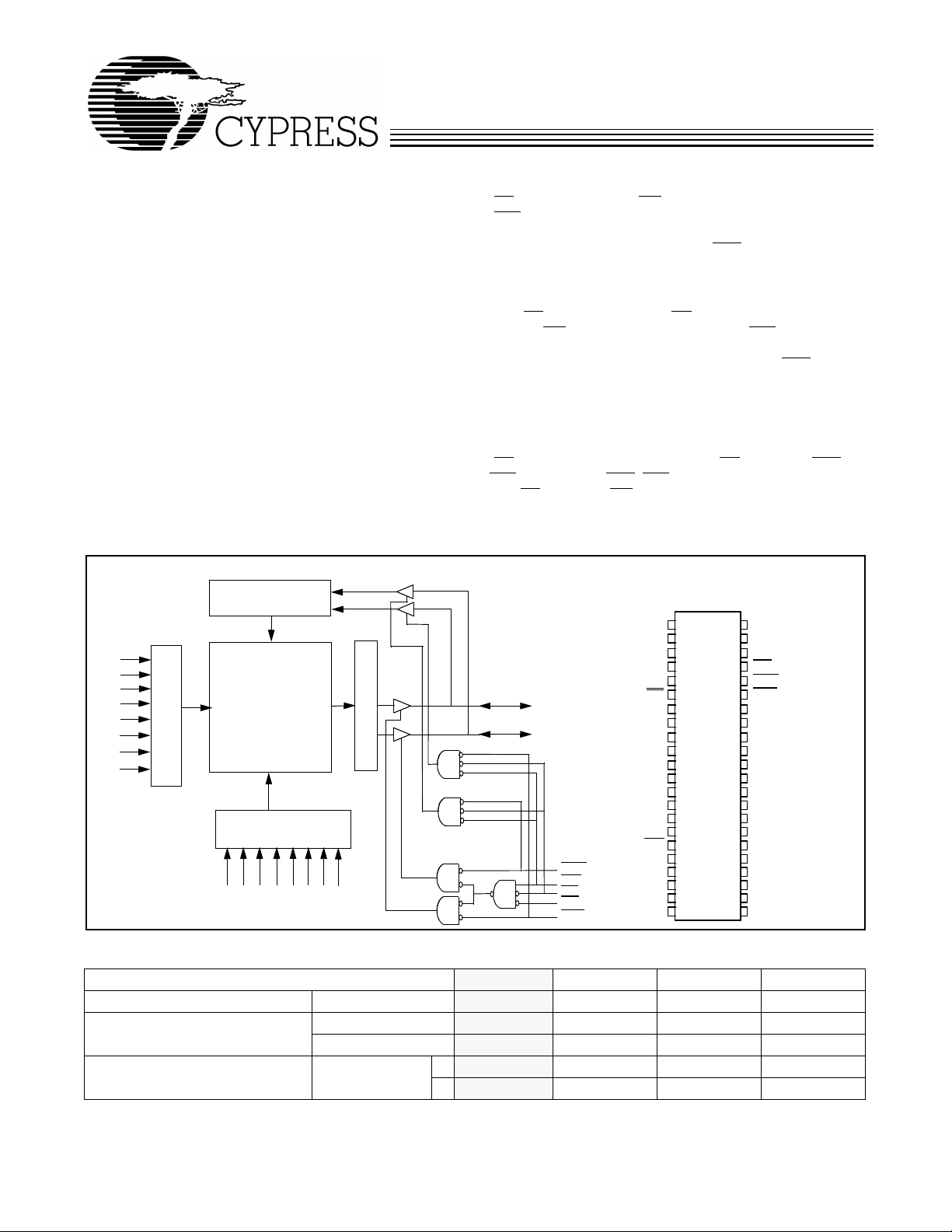
Logic Block Diagram
DATA IN DRIVERS
A
7
A
6
A
5
A
4
A
3
A
2
A
1
A
0
ROW DECODER
64K x 16
RAM Array
512 X 2048
COLUMN DECODER
8
A
A
9
A10A11A
I/O
–I/O
1
8
SENSE AMPS
I/O9–I/O
16
BHE
WE
12
14
15
A13A
A
CE
OE
BLE
Pin Configurations
SOJ / TSOP II
Top View
44
I/O
I/O
I/O
I/O
V
V
I/O
I/O
I/O
I/O
WE
A
A
A
A
A
A
A
A
A
CE
CC
NC
SS
15
14
13
12
1
4
2
3
3
2
4
1
5
0
6
7
1
8
2
9
3
10
4
11
12
13
5
14
6
15
7
16
8
17
18
19
20
21
22
A
5
43
A
6
42
A
7
41
OE
40
BHE
39
BLE
38
I/O
16
37
I/O
15
36
I/O
14
35
I/O
13
34
V
SS
33
V
CC
32
I/O
12
I/O
31
11
30
I/O
10
29
I/O
9
28
NC
27
A
8
26
A
9
A
25
10
A
24
11
23
NC
Selection Guide
7C1021BV-8 7C1021BV-10 7C1021BV-12 7C1021BV-15
Maximum Access Time (ns) 81012 15
Maximum Operating Current (mA) Commercial 170 160 150 140
Industrial 190 180 170 160
Maximum CMOS Standby Current
(mA)
Shaded areas contain advance information.
Note:
1. For guidelines on SRAM system design, please refer to the ‘System Design Guidelines’ Cypress application note, available on the internet at www.cypress.com.
Commercial 555 5
L 0.500 0.500 0.500 0.500
Cypress Semiconductor Corporation • 3901 North First Street • San Jose • CA 95134 • 408-943-2600
Document #: 38-05148 Rev. *A Revised September 13, 2002
Pin Configurations
CY7C1021BV33
Mini BGA
(Top View)
123456
BLE
I/O
I/O
V
V
I/O
I/O
NC
A
A
NC
A
A
A
A
A
15
13
10
1
4
6
7
A
2
CE
I/O
2
I/O
V
4
V
I/O
5
I/O6I/O
WE
I/O
A
11
NC
I/O
I/O
CC
SS
NC
A
OE
0
A
BHE
I/O
I/O
I/O
I/O
NC
A
3
A
5
11
NC
12
NC
13
A
14
14
A
12
A
9
8
9
10
SS
CC
15
16
A
B
1
C
3
D
E
F
7
G
8
H
Maximum Ratings
(Above which the useful life may be impaired. For user guidelines, not tested.)
Storage Temperature .................................–65°C to +150°C
Ambient Temperature with
Power Applied.............................................–55°C to +125°C
Supply Voltage on V
DC Voltage Applied to Outputs
in High Z State
[2]
DC Input Voltage
to Relative GND
CC
......................................–0.5V to VCC+0.5V
[2]
...................................–0.5V to VCC+0.5V
Note:
2. Mimimum v oltage is–2.0V for pulse durations of less than 20 ns.
[2]
....–0.5V to +4.6V
Current into Outputs (LOW) ........................................20 mA
Stat ic Disc ha rge Voltage............................................>2001V
(per MIL-STD-883, Method 3015)
Latch-Up Current.....................................................>200 mA
Operating Range
Range Ambient Temperature V
Commercial 0°C to +70°C 3.3V ± 10%
Industrial –40°C to +85°C 3.3V ± 10%
CC
Document #: 38-05148 Rev. *A Page 2 of 11
Electrical Characteristics Ov er the Op erat ing Range
7C1021BV-8 7C1021BV-10 7C1021BV-12 7C1021BV-15
Parameter Description Test Conditions
V
OH
V
OL
V
IH
V
IL
I
IX
I
OZ
I
CC
I
SB1
I
SB2
Shaded areas contain advance information.
Output HIGH
Voltage
Output LOW
Voltage
Input HIGH
Voltage
Input LOW
[2]
Voltage
Input Load
Current
Output Leakage
Current
VCC Operating
Supply Current
Automatic CE
Power-Down
Current
—TTL Inputs
Automatic CE
Power-Down
Current
—CMOS Inputs
VCC = Min.,
I
= –4.0 mA
OH
2.4 2.4 2.4 2.4 V
VCC = Min., IOL = 8.0 mA 0.4 0.4 0.4 0.4 V
2.2 VCC+
−0.3 0.8 −0.3 0.8 –0.3 0.8 –0.3 0.8 V
GND < VI < V
CC
GND < VI < VCC,
Output Disabled
VCC = Max.,
I
= 0 mA,
OUT
MAX
= 1/t
f = f
Com 170 160 150 140 mA
Ind 190 120 170 160 mA
RC
Max. VCC,
> V
CE
IH
VIN > VIH or
VIN < VIL, f = f
MAX
Max. VCC,
CE > VCC – 0.3V,
> VCC – 0.3V,
V
IN
< 0.3V,
or V
IN
f = 0
L 500 500 500 500 µA
CY7C1021BV33
UnitMin. Max. Min. Max. Min. Max. Min. Max.
2.2 VCC+
0.3V
0.3V
−1 +1 −1+1–1 +1 –1 +1 µA
−1 +1 −1+1–1 +1 –1 +1 µA
40 40 40 40 mA
55 5 5 mA
2.2 VCC+
0.3V
2.2 VCC+
0.3V
V
Capacitance
[3]
Parameter Description Test Conditions Max. Unit
C
IN
C
OUT
Note:
3. Tested initially and after any design or process changes that may affect these parameters.
Input Capacitance TA = 25°C, f = 1 MHz 6 pF
Output Capacitance 8 pF
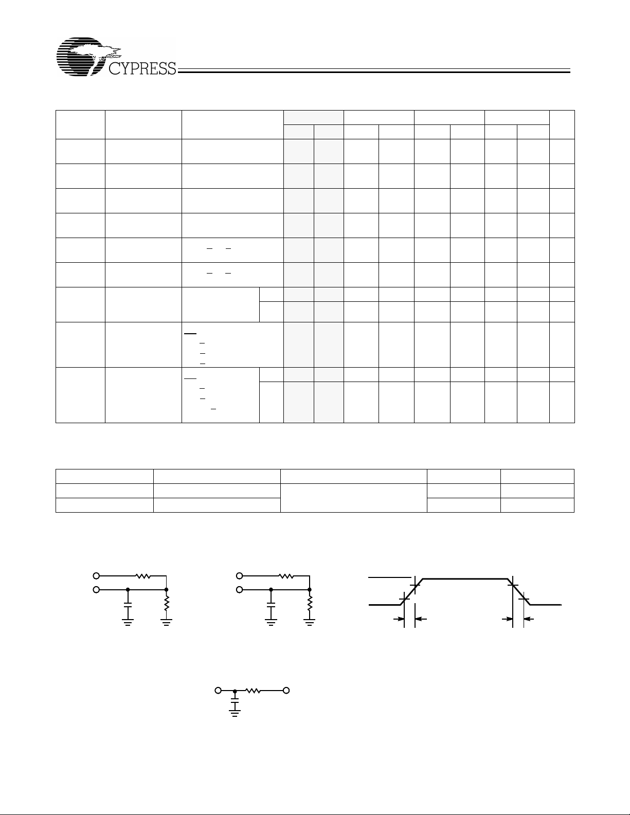
AC Test Loads and Waveforms
(b)
R 317Ω
1.73V
R2
351Ω
3.0V
GND
Rise Time: 1 V/ns
ALL INPUT PULSES
90%
10%
3.3V
OUTPUT
INCLUDING
JIG AND
SCOPE
Equivalent to:
30 pF
R 317Ω
(a)
THÉVENIN
EQUIVALENT
OUTPUT
R2
351Ω
OUTPUT
3.3V
5 pF
INCLUDING
JIG AND
SCOPE
167
30 pF
90%
10%
Fall Time: 1 V/ns
Document #: 38-05148 Rev. *A Page 3 of 11
CY7C1021BV33
Switching Characteristics
Parameter Description
READ CYCLE
t
RC
t
AA
t
OHA
t
ACE
t
DOE
t
LZOE
t
HZOE
t
LZCE
t
HZCE
t
PU
t
PD
t
DBE
t
LZBE
t
HZBE
WRITE CYCLE
t
WC
t
SCE
t
AW
t
HA
t
SA
t
PWE
t
SD
t
HD
t
LZWE
t
HZWE
t
BW
Shaded areas contain advance information.
Read Cycle Time 8 10 12 15 ns
Address to Data Valid 81012 15 ns
Data Hold from Address Change 3 3 3 3 ns
CE LOW to Data Valid 81012 15 ns
OE LOW to Data Valid 446 7 ns
OE LOW to Low Z 0 0 0 0 ns
OE HIGH to High Z
CE LOW to Low Z
CE HIGH to High Z
CE LOW to Power-Up 0 0 0 0 ns
CE HIGH to Power-Down 12 12 12 15 ns
Byte Enable to Data Valid 4 5 6 7 ns
Byte Enable to Low Z 0 0 0 0 ns
Byte Disable to High Z 456 7 ns
[7]
Write Cycle Time 8 10 12 15 ns
CE LOW to Write End 7 8 9 10 ns
Address Set-Up to Write End 6 7 8 10 ns
Address Hold from Write End 0 0 0 0 ns
Address Set-Up to Write Start 0 0 0 0 ns
WE Pulse Width 6 8 8 10 ns
Data Set-Up to Write End 4 6 6 8 ns
Data Hold from Write End 0 0 0 0 ns
WE HIGH to Low Z
WE LOW to High Z
Byte Enable to End of Write 8 8 8 9 ns
[4]
Over the Operating Range
7C1021BV-8 7C1021BV-10 7C1021BV-12 7C1021BV-15
[5, 6]
[6]
[5, 6]
[6]
[5, 6]
3 3 3 3 ns
3 3 3 3 ns
UnitMin. Max. Min. Max. Min. Max. Min. Max.
456 7 ns
456 7 ns
456 7 ns
Data Retention Characte ristics Over the Operating Range (L version only)
LZOE
[8]
, and t
HZWE
Min. Max. Unit
100 µA
RC
is less than t
for any given device.
LZWE
ns
Parameter Description Conditions
V
DR
I
CCDR
[9]
t
CDR
[10]
t
R
Notes:
4. T est conditions assume signal transition time of 3 ns or less, timing reference levels of 1.5V, input pulse levels of 0 to 3.0V, and output loading of the specified
I
and 30-pF load cap aci tance.
OL/IOH
5. t
6. At any given temperature and voltage condition, t
7. The in ter na l wr i t e ti m e of th e me mo ry is de fi ne d by t h e ov er la p of CE LOW , WE LOW and BHE / BLE LOW. CE, WE an d BHE / BLE must be LOW to initiate a wr ite,
8. No input may exceed V
9. Tested initially and after any design or process changes that may affect these parameters.
10. t
, t
HZOE
HZBE
and the transition of these s ignals can te rminate the wri te. The input data set- up and hold t iming should be referenced to the leadin g edge of the signal that terminates t he write.
< 3 ns for the -12 and -15 s peeds. tr < 5 ns for the -2 0 and s lower s peeds.
r
VCC for Data Retention 2.0 V
Data Retention Current Com’l VCC = VDR = 2.0V,
> VCC – 0.3V ,
CE
> VCC – 0.3V or VIN < 0.3V
V
IN
Chip Deselect to Data Retention Time 0 ns
Operation Recovery Time t
, t
HZCE
, and t
are specified with a load cap acitance of 5 pF as in part (b) of AC Test Loads. Trans ition is measure d ±50 0 mV from stead y-st ate vol tag e.
HZWE
+ 0.5V.
CC
HZCE
is less than t
LZCE
, t
HZOE
is less than t
Document #: 38-05148 Rev. *A Page 4 of 11

Data Retention Waveform
V
CC
CE
Switching Waveforms
t
CDR
CY7C1021BV33
DATA RETENTION MODE
V
> 2V
DR
3.0V3.0V
t
R
Read Cycle No. 1
ADDRESS
DATA OUT
Read Cycle No. 2
ADDRESS
CE
OE
BHE, BLE
DATA OUT
V
CC
SUPPLY
CURRENT
[11, 12]
t
RC
t
t
OHA
AA
PREVIOUS DATA VALID DATA VALID
t
LZCE
t
PU
[12, 13]
t
ACE
t
DOE
t
LZOE
t
DBE
t
LZBE
t
RC
t
HZOE
DATA VALID
(OEControlled)
HIGH IMPEDANCE
50%
t
HZCE
t
HZBE
t
PD
50%
HIGH
IMPEDANCE
I
ICC
CC
I
ISB
SB
Notes:
11. Device is continuously selected. OE
is HIGH for read cycle .
12. WE
13. Address valid prior to or coincident with CE
, CE, BHE and/or BHE = VIL.
transition LOW .
Document #: 38-05148 Rev. *A Page 5 of 11

Switching Waveforms (continued)
CY7C1021BV33
Write Cycle No. 1 (CE
ADDRESS
CE
WE
BHE, BLE
DATA I/O
Controlled)
t
SA
[14, 15]
t
AW
t
WC
t
SCE
t
PWE
t
BW
t
HA
t
SD
t
HD
Write Cycle No. 2 (BLEor BHE Controlled)
ADDRESS
t
,BLE
BHE
WE
CE
DATA I/O
Notes:
14. Data I/O is high impedance if OE
15. If C E
goes HIGH simultaneous ly with WE going HIGH , the outpu t remains in a high-im pedance state .
SA
or BHE and/or BLE = VIH.
t
WC
t
BW
t
AW
t
PWE
t
SCE
t
SD
t
HA
t
HD
Document #: 38-05148 Rev. *A Page 6 of 11

Switching Waveforms (continued)
CY7C1021BV33
Write Cycle No. 3
ADDRESS
CE
WE
BHE
, BLE
DATA I/O
Truth Table
Controlled, LOW)
(WE
t
SA
t
WC
t
SCE
t
AW
t
BW
t
HZWE
t
PWE
t
SD
t
HA
t
HD
t
LZWE
CE OE WE BLE BHE I/O1–I/O
8
I/O9–I/O
16
Mode Power
H X X X X High Z High Z Power-Down Standb y (ISB)
L L H L L Data Out Data Out Read - All bits Active (ICC)
L H Data Out High Z Read - Lower bits only Active (ICC)
H L High Z Data Out Read - Upper bits only Active (ICC)
L X L L L Data In Data In Write - All bits Active (ICC)
L H Data In High Z Write - Lower bits only Active (ICC)
H L High Z Data In Write - Upper bits only Active (ICC)
L H H X X High Z High Z Selected, Output s Disabled Active (ICC)
L X X H H High Z High Z Selected, Outputs Disabled Active (ICC)
Document #: 38-05148 Rev. *A Page 7 of 11

CY7C1021BV33
Ordering Information
Speed (ns) Ordering Code
8 CY7C1021BV33-8BAC BA48A 48-Ball Mini Ball Grid Array (7.00 mm x 7.00 mm) Commercial
CY7C1021BV33-8VC V34 44-Lead (400-Mil) Molded SOJ
CY7C1021BV33L-8VC V34 44-Lead (400-Mil) Molded SOJ
CY7C1021BV33-8ZC Z44 44-Lead TSOP Type II
CY7C1021BV33L-8ZC Z44 44-Lead TSOP Type II
10 CY7C1021BV33-10BAC BA48A 48-Ball Mini Ball Grid Array (7.00 mm x 7.00 mm) Commercial
CY7C1021BV33-10VC V34 44-Lead (400-Mil) Molded SOJ
CY7C1021BV33L-10VC V34 44-Lead (400-Mil) Molded SOJ
CY7C1021BV33-10ZC Z44 44-Lead TSOP Type II
CY7C1021BV33L-10ZC Z44 4 4-Lead TSOP Type II
12 CY7C1021BV33-12BAC BA48A 48-Ball Mini Ball Grid Array (7.00 mm x 7.00 mm) Commercial
CY7C1021BV33-12VC V34 44-Lead (400-Mil) Molded SOJ
CY7C1021BV33L-12VC V34 44-Lead (400-Mil) Molded SOJ
CY7C1021BV33-12ZC Z44 44-Lead TSOP Type II
CY7C1021BV33L-12ZC Z44 4 4-Lead TSOP Type II
CY7C1021BV33-12BAI BA48A 48-Ball Mini Ball Grid Array (7.00 mm x 7.00 mm) Industrial
CY7C1021BV33-12VI V34 44-Lead (400-Mil) Molded SOJ
15 CY7C1021BV33-15BAC BA48A 48-Ball Mini Ball Grid Array (7.00 mm x 7.00 mm) Commercial
CY7C1021BV33L-15BAC BA48A 48-Ball Mini Ball Grid Array (7.00 mm x 7.00 mm)
CY7C1021BV33-15VC V34 44-Lead (400-Mil) Molded SOJ
CY7C1021BV33L-15VC V34 44-Lead (400-Mil) Molded SOJ
CY7C1021BV33-15ZC Z44 44-Lead TSOP Type II
CY7C1021BV33L-15VC Z44 44-Lead TSOP Type II
CY7C1021BV33-15BAI BA48A 48-Ball Mini Ball Grid Array (7.00 mm x 7.00 mm) Industrial
CY7C1021BV33L-15BAI BA48A 48-Ball Mini Ball Grid Array (7.00 mm x 7.00 mm)
CY7C1021BV33-15VI V34 44-Lead (400-Mil) Molded SOJ
CY7C1021BV33L-15ZI Z44 44-Lead TSOP Type II
Shaded areas contain advance information.
Package
Name Package Type
Operating
Range
Document #: 38-05148 Rev. *A Page 8 of 11

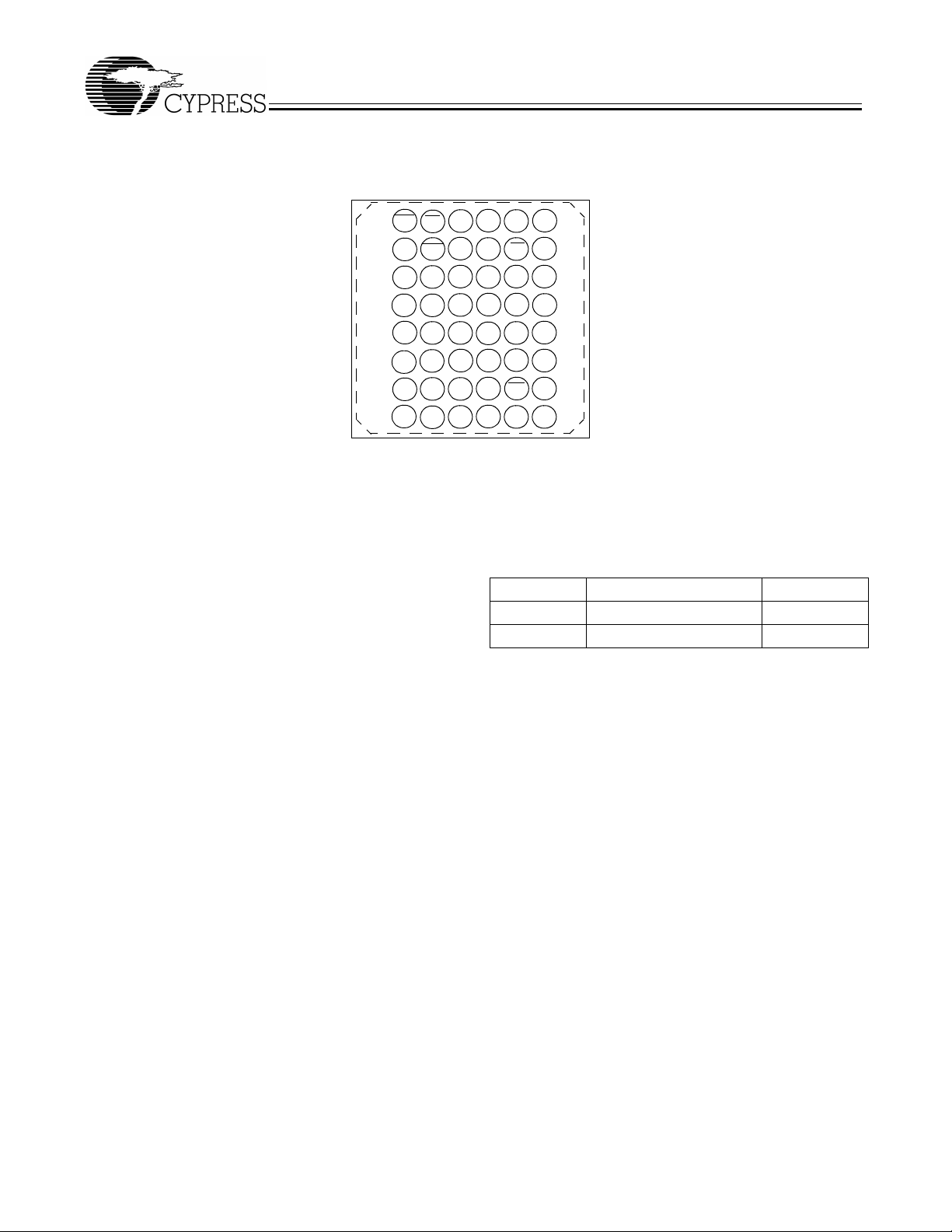
Package Diagrams
48-Ball (7.00 mm x 7.00 mm x 1.2 mm) FBGA BA48A
CY7C1021BV33
51-85096-*E
Document #: 38-05148 Rev. *A Page 9 of 11

Package Diagrams (continued)
CY7C1021BV33
44-Lead (400-Mil) Mo lded SOJ V3 4
44-Pin TSOP II Z44
51-85082-*B
51-85087-A
All product and company names mentioned in this document may be the trademarks of their respective holders.
Document #: 38-05148 Rev. *A Page 10 of 11
© Cypress Semiconductor Corporation, 2002. The information contained herein is subject to change without notice. Cypress Semiconductor Corporation assumes no responsibility for the use
of any circuitry other than cir cuitry embodi ed in a Cypress S emiconductor product . Nor does it convey or imply any license un der patent or other righ ts. Cypre ss Semiconductor does not autho rize
its products for use as critical components in life-support systems where a malfunction or failure may reasonably be expected to result in significant injury to the user. The inclusion of Cypress
Semiconductor products in life-support systems application implies that the manufacturer assumes all risk of such use and in doing so indemnifies Cypress Semiconductor against all charges.

Document History Page
Document Title: CY7C1021BV33 64K x 16 Static RAM
Document Number: 38-05148
REV. ECN NO.
** 109892 09/22/01 SZV Change from Spec number: 38-00954 to 38-05148
*A 116474 09/16/02 CEA Add applications foot note to data sheet, page 1.
Issue
Date
Orig. of
Change Description of Change
CY7C1021BV33
Document #: 38-05148 Rev. *A Page 11 of 11
 Loading...