

Datasheet CY7C056V-15AC, CY7C056V-12BAC, CY7C056V-12AC, CY7C057V-20BAI, CY7C057V-20BAC Datasheet (Cypress Semiconductor)
...
3.3V 16K/32K x 36
FLEx36™ Asynchronous Dual-Port Static RAM
CY7C056V
CY7C057V
PRELIMINARY
Cypress Semiconductor Corporation
• 3901 North First Street • San Jose • CA 95134 • 408-943-2600
April 27, 2000
1
Features
• True dual-ported memory cells which allow simultaneous access of the same memory locat ion
• 16K x 36 organizat ion (CY7C056V)
• 32K x 36 organizat ion (CY7C057V)
• 0.25-micron CMOS for optimum speed/power
• High-speed access: 10/12/15/20 ns
• Low op e ratin g po w er
—
Active: I
CC
= 260 mA (typical)
—Standby: I
SB3
= 10 µA (typical)
• Fully asy nchronous operation
• Automatic power-down
• Expandable data bus to 72 bits or more using Master/Slave Chip Sel ect when using more th an one device
• On-Chip arbitration logic
• Semaphor es included to permit software handshak ing
between ports
•INT
flag for port-to-port communication
• Byte Select on Left Port
• Bus Matching on Right Port
• Depth Expansion via dual chip enables
• Pin select for Master or Slave
• Commercial and Industrial Temperature Ranges
• Compact pac kage
—144-Pin TQFP (20 x 20 x 1.4 mm)
—
172-Ball BGA (1.0 mm pitch) (15 x 15 x .51 mm)
Notes:
1. A
0–A13
for 16K; A0–A14 for 32K devices.
2. BUSY
is an output in Master mode and an input in Slave mode.
R/W
L
CE
0L
CE
1L
OE
L
I/O
Control
Address
Decode
BUSY
L
CE
L
Interrupt
Semaphore
Arbitration
SEM
L
INT
L
M/S
R/W
R
CE
0R
CE
1R
OE
R
CE
R
Logic Block Dia gram
A0L–A
13/14L
True Dual-Ported
RAM Array
BUSY
R
SEM
R
INT
R
Address
Decode
A
0R–A13/14R
[2]
[2]
[1] [1]
14/15 14/15
14/15 14/15
Left
Port
Control
Logic
I/O
18L
–I/O
26L
9
I/O
27L
–I/O
35L
9
I/O0L–I/O
8L
9
I/O9L–I/O
17L
9
Right
Port
Control
Logic
I/O
Control
9
9
I/O
R
9
9
Bus
Match
9/18/36
BA
BM
SIZE
WA
B
0–B3
For the most recent information, visit the Cypress web site at www.cypress.com

CY7C056V
CY7C057V
2
PRELIMINARY
Functional Description
The CY7C056V and CY7C057V are low-power CMOS 16K
and 32K x 36 dual-port static RAMs. Various arbitration
schemes are included on the devices to handle situations
when multipl e proces sor s access t he s ame piece of data. Tw o
ports are provided , pe rmitting i ndep endent, asyn chronous access for reads and writes to any location in memory. The devices can be utilized as standalone 36-bit dual-port static
RAMs or multip le devi ces can b e combined in o rder to fu nction
as a 7 2-bit o r wider master /sla v e d ual -port stati c RAM. An M/S
pin is prov ided f or impl ementi ng 72-bi t or wide r memory applications without the need for separate master and s lave devices or additional discrete logi c. Application areas include interprocessor/multiprocessor designs, communications status
buffering, and dual-port video/graphics memory.
Each port has independent control pins: Chip Enable (CE
)
[3]
,
Read or Write Enable (R/W
), and Output Enable (OE). Two
flags are provided on each port (BUSY
and INT). BUSY signals that the port is trying to access t he same location cur rently
being accessed b y the other port. TheInterrupt Flag (INT
) permits communicati on between ports or systems by means of a
mail box. The semaphores are used to pass a flag, or token,
from one port to the oth er to i ndicat e that a shared resource i s
in use. The semaphore logic is comprised of eight shared
latches. Only one side can control the latch (semaphore) at
any time. Control of a semaphore indicates that a shared resource is in use. An automatic Power-Down feature is controlled independently on each port by Chip Select (CE
0
and
CE
1
) pins.
The CY7C056V and CY7C057V are available in 144-Pin Thin
Quad Plastic Flatpack (TQFP) and 172-Ball Ball Grid Array
(BGA) packages.
Note:
3. CE
is LOW when CE0 ≤ VIL and CE1 ≥ VIH.

CY7C056V
CY7C057V
3
PRELIMINARY
Pin Configurations
Notes:
4. This pin is A14L for CY7C057V.
5. This pin is A14R for CY7C057V.
144-PinThin Quad Flatpack(TQFP)
Top View
I/O32L
I/O33R
I/O23L
I/O33L
2
3
4
I/O34L I/O34R
5
I/O35L I/O35R
6
A0L
A0R
7
A1L A1R
8
A2L
A2R
9
A3L
A3R
10
A4L
A4R
11
A5L
A5R
12
A6L
A6R
13
A7L
108
A7R
14
B0
107
BM
15
B1
106
SIZE
16
B2
105
WA
17
B3
104
BA
18
OEL
103
OER
19
R/WL
102
R/WR
20
VDD
101
VDD
21
VSS
100
VSS
22
VSS
99
VDD
23
CE0L
98
CE0R
24
CE1L
97
CE1R
25
M/S
96
VDD
26
SEML
95
SEMR
27
INTL
94
INTR
28
BUSYL
93
BUSYR
29
A8L
92
A8R
30
A9L
91
A9R
31
A10L
90
A10R
32
A11L
89
A11R
33
A12L
88
A12R
34
A13L
87
A13R
35
NC
86
NC
36
I/O26L
85
I/O26R
I/O25L
84
I/O25R
I/O24L
83
I/O24R
82
81
414243
44
I/O22L
I/O31L
45
VSS
VSS
46
I/O21L
I/O30L
47
I/O20L
I/O29L
48
I/O19L
I/O28L
49
I/O18L
I/O27L
50
VDD
VDD
51
I/O8L
I/O17L
52
I/O7L
I/O16L
53
I/O6L
I/O15L
54
I/O5L
I/O14L
55
VSS
VSS
56
I/O4L
I/O13L
57
I/O3L
I/O12L
58
I/O2L
143
I/O11L
59
I/O1L
142
I/O10L
60
I/O0L
141
I/O9L
61
I/O0R
140
I/O9R
62
I/O1R
139
I/O10R
63
I/O2R
138
I/O11R
64
I/O3R
137
I/O12R
65
I/O4R
136
I/O13R
66
VSS
135
VSS
67
I/O5R
134
I/O14R
68
I/O6R
133
I/O15R
69
I/O7R
132
I/O16R
70
I/O8R
131
I/O17R
71
VDD
130
VDD
72
I/O18R
129
I/O27R
123
I/O19R
128
I/O28R
122
I/O20R
127
I/O29R
121
I/O21R
126
I/O30R
120
VSS
125
VSS
119
I/O22R
124
I/O31R
118
I/O23R
I/O32R
117
116
373839
40
80
79
78
77
76
75
74
73
115
114
113
112
111
110
109
144
1
CY7C056V (16K x 36)
CY7C057V (32K x 36)
[4]
[5]
CY7C056V
CY7C057V
4
PRELIMINARY
Pin Configurations
(continued)
172-Ba ll B a ll G r id Ar ray (BG A )
T op View
1 23 4567891011121314
A
I/O32L I/O30L NC VSS I/O13L VDD I/O11L I/O11R VDD I/O13R VSS NC I/O30R I/O32R
B
A0L I/O33L I/O29 I/O17L I/O14L I/O12L I/O9L I/O9R I/O12R I/O14R I/O17R I/O29R I/O33R A0R
C
NC A1L I/O31L I/O27L NC I/O15L I/O10L I/O10R I/O15R NC I/O27R I/O31R A1R NC
D
A2L A3L I/O35L I/O34L I/O28L I/O16L VSS VSS I/O16R I/O28R I/O34R I/O35R A3R A2R
E
A4L A5L NC B0L NC NC NC NC BM NC A5R A4R
F
VDD A6L A7L B1L NC NC SIZE A7R A6R VDD
G
OEL B2L B3L CE0L CE0R BA WA OER
H
VSS R/WL A8L CE1L CE1R A8R R/WRVSS
J
A9L A10L VSS M/S NC NC VDD VDD A10R A9R
K
A11L A12L NC SEML NC NC NC NC SEMR NC A12R A11R
L
BUSYL A13L INTL I/O26L I/O25L I/O19L VSS VSS I/O19R I/O25R I/O26R INTR A13R BUSYR
M
NC NC I/O22L I/O18L NC I/O7L I/O2L I/O2R I/O7R NC I/O18R I/O22R NC NC
N
I/O24L I/O20L I/O8L I/O6L I/O5L I/O3L I/O0L I/O0R I/3R I/O5R I/O6R I/O8R I/O20R I/O24R
P
I/O23L I/O21L NC VSS I/O4L VDD I/O1L I/O1R VDD I/O4R VSS NC I/O21R I/O23R
[5]
[4]
CY7C056V
CY7C057V
5
PRELIMINARY
Maximum Ratings
(Above which the useful life m ay be impaired. F or user guidelines, not tested.)
Storage Tem perature ........................... .. ....–65
°
C to +150°C
Ambient Temperature with
Power Applied.............................................–55
°
C to +125°C
Supply Voltage to Ground Potential............... –0.5V to +4.6V
DC V oltage Applied to
Outputs in High Z State ...........................–0.5V to V
DD
+0.5V
DC Input Voltage...................................–0. 5V to V
DD
+0.5V
[6]
Output Current into Outputs (LOW)............................. 20 mA
Static Discharge Voltage.................... ...................... >2001V
Latch-Up Current............. .. .............. ....................... >200 mA
Shaded areas contain advance information.
Note:
6. Pulse width < 20 ns.
Selectio n Guide
CY7C056V
CY7C057V
-10
CY7C056V
CY7C057V
-12
CY7C056V
CY7C057V
-15
CY7C056V
CY7C057V
-20
Maximum Access Time (ns) 10 12 15 20
Typical Operat ing Current (mA) 260 250 240 230
Typical Standb y Current for I
SB1
(mA) (Both Ports TTL Level) 60 55 50 45
Typical Standb y Current for I
SB3
(µA) (Both Ports CMOS
Level)
10 µA10 µA 10 µA 10 µA
Pin Definitions
Left Port Right Port Description
A0L–A
13/14L
A0R–A
13/14R
Address (A0–A13 for 16K ; A0–A14 for 32K devices)
SEML SEM
R
Semaphore Enable
CE0L, CE
1L
CE0R, CE
1R
Chip Enable (CE is LOW when CE0 ≤ VIL and CE1 ≥ VIH)
INT
L
INT
R
Interrupt Flag
BUSY
L
BUSY
R
Busy Flag
I/O0L–I/O
35L
I/O0R–I/O
35R
Data Bus Input/Output
OE
L
OE
R
Output Enable
R/W
L
R/W
R
Read/Write Enable
B0–B
3
Byte Select Inputs. Asserting these signals enables read and write oper-
ations to the corresponding bytes of the memory array.
BM, SIZE See Bus Matching for detai ls.
WA, B A See Bus Matching for detai ls.
M/S Master or Slave Select
V
SS
Ground
V
DD
Power
Operating Range
Range
Ambient
Temperature
V
DD
Commercial 0°C to +70°C 3.3V ± 165 mV
Industrial –40°C to +85°C 3.3V ± 165 mV
CY7C056V
CY7C057V
6
PRELIMINARY
Shaded areas contain advance information.
Notes:
7. Cross Levels are V
DD
– 0.2V< VZ<0.2V.
8. Deselection for a port occurs if CE
0
is HIGH or if CE1 is LOW.
9. f
MAX
= 1/tRC = All inputs cycling at f = 1/tRC (except Output Enable). f = 0 means no address or control lines change. This applies only to inputs at CMOS level
standby I
SB3
.
10. Tested initially and after any design or process changes that may affect these parameters.
Electrical Characteristics
Over the Operating Range
[7, 8]
Parameter Description
CY7C056V
CY7C057V
Unit
-10 -12 -15 -20
Min.
Typ.
Max.
Min.
Typ.
Max.
Min.
Typ.
Max.
Min.
Typ.
Max.
V
OH
Output HIGH Voltage
(V
DD
= Min. , I
OH
= –4.0 mA) 2.4 2.4 2.4 2.4 V
V
OL
Output LO W Voltage
(V
DD
= Min. , I
OL
= +4.0 mA) 0.4 0.4 0.4 0.4 V
V
IH
Input HIGH Voltage 2.0 2.0 2.0 2.0 V
V
IL
Input LOW Voltage 0.8 0.8 0.8 0.8 V
I
OZ
Output Leakage Curr ent -10 10 –10 10 –10 10 –10 10 µA
I
CC
Operating Cur rent (V
DD
=
Max., I
OUT
= 0 mA) Outputs
Disabled
Com’l. 260 410 250 385 240 360 230 340 mA
Indust.
265 385 mA
I
SB1
Standby Cur rent (Both P orts
TTL Lev el and Deselected)
f = f
MAX
Com’l. 60 80 55 75 50 70 45 65 mA
Indust.
65 95 mA
I
SB2
Standby Current (One Port
TTL Lev el and Deselected)
f = f
MAX
Com’l. 185 250 180 240 175 230 165 210 mA
Indust.
190 255 mA
I
SB3
Standby Cur rent (Both P orts
CMOS Level and Deselected) f =0
Com’l. 0.01 1 0.01 1 0.01 1 0.01 1 mA
Indust.
0.01 1 mA
I
SB4
Standby Current (One Port
CMOS Level and Deselected) f = f
MAX
[9]
Com’l. 170 220 160 210 155 200 145 180 mA
Indust.
170 215 mA
Capacitance
[10]
Parameter Description Test Conditions Max. Unit
C
IN
Input Capacitance TA = 25°C, f = 1 MHz,
V
DD
= 3.3V
10 pF
C
OUT
Output Capacitance 10 pF
CY7C056V
CY7C057V
7
PRELIMINARY
Notes:
11. External AC Test Load Capacitance = 10 pF.
12. (Internal I/O pad Capacitance = 10 pF) + AC Test Load.
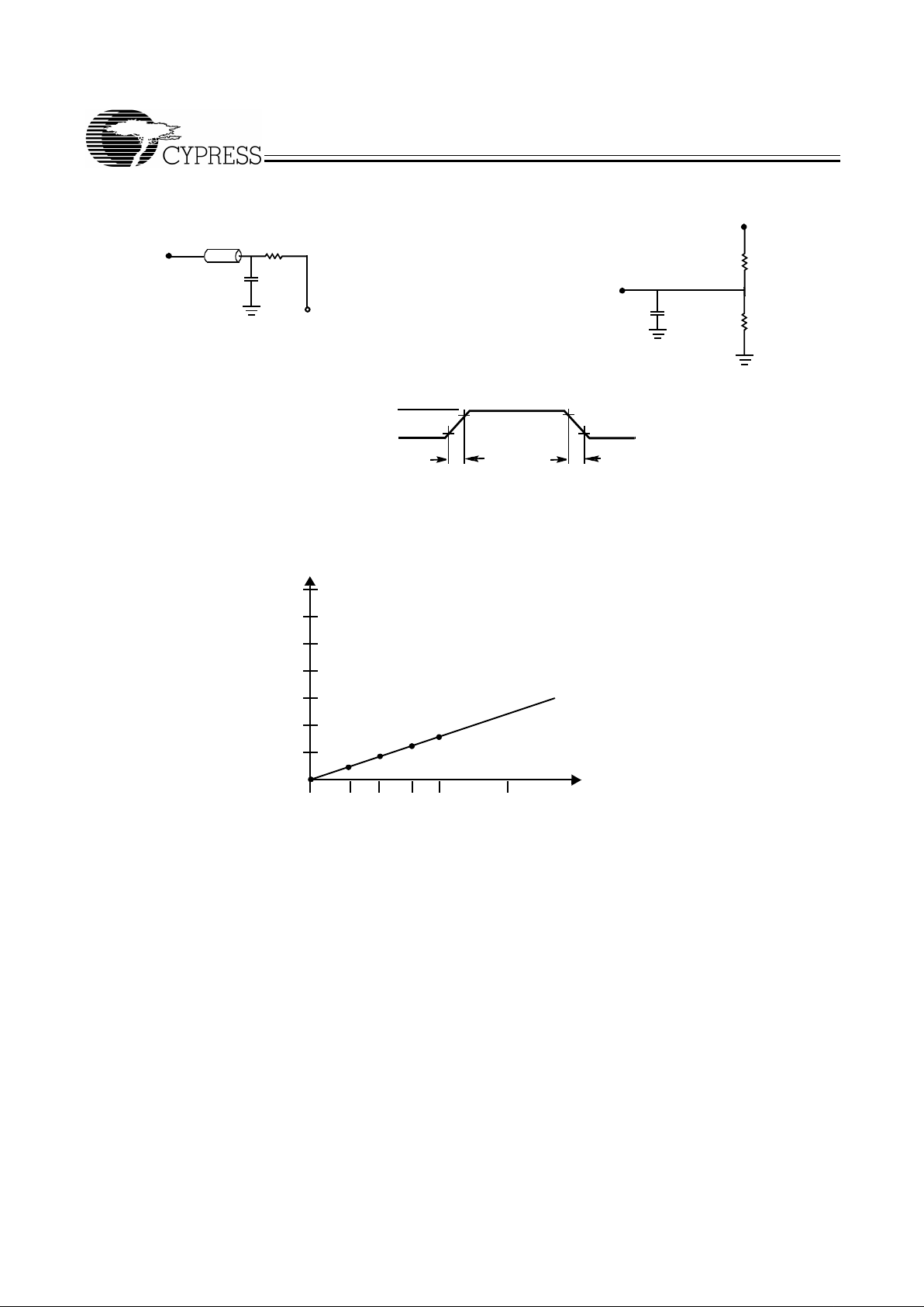
AC Test Load and Waveforms
VTH=1.5V
OUTPUT
C
(a) Normal Load (Load 1)
R = 50
Ω
Z0 = 50
Ω
[11]
3.0V
V
SS
90%
90%
10%
3ns
3
ns
10%
≤
≤
ALL INPUT PULSES
3.3V
OUTPUT
C = 5 pF
(b) Three-State Delay (Load 2)
R2 = 435
Ω
R1 = 590
Ω
(b) Load Derating Curve
1
2
3
4
5
6
7
30 60 80 100 200
∆
(ns) for access time
Capacitance (pF)
20
[12]

CY7C056V
CY7C057V
8
PRELIMINARY
Switching Characteristics
Over the Operating Range
[13]
Parameter Description
CY7C056V
CY7C057V
Unit
-10 -12
-15 -20
Min. Max. Min. Max.
Min. Max. Min. Max.
Read Cycle
t
RC
Read Cycle Time 10 12 15 20 ns
t
AA
Address to Dat a Valid 10 12 15 20 ns
t
OHA
Output Hold From Address
Change
333 3 ns
t
ACE
[3, 14]
CE LOW to Data Valid 10 12 15 20 ns
t
DOE
OE LOW to Data Valid 6 8 10 12 ns
t
LZOE
[3, 15, 16, 17]
OE Low to Low Z 0 0 0 0 ns
t
HZOE
[3, 15, 16, 17]
OE HIGH to High Z 8 10 10 12 ns
t
LZCE
[3, 13, 16, 17]
CE LOW to Low Z 3 3 3 3 ns
t
HZCE
[3, 15, 16, 17]
CE HIGH to High Z 8 10 10 12 ns
t
LZBE
Byte Enable to Low Z 3 3 3 3 ns
t
HZBE
Byte Enable to High Z 8 10 10 12 ns
t
PU
[3, 17]
CE LOW to Power-Up 0 0 0 0 ns
t
PD
[3, 17]
CE HIGH to Power-Down 10 12 15 20 ns
t
ABE
[14]
Byte Enable Access Time 10 12 15 20 ns
Write Cycle
t
WC
Write Cycle Time 10 12 15 20 ns
t
SCE
[3, 14]
CE LOW to Write End 7.5 10 12 15 ns
t
AW
Address Valid to Write End 7.5 10 12 15 ns
t
HA
Address Hold From Write
End
000 0 ns
t
SA
[14]
Address Set-Up to Write
Start
000 0 ns
t
PWE
Write Pulse Width 7.5 10 12 15 ns
t
SD
Data Set-Up to Writ e E n d 7.5 10 10 15 ns
t
HD
Data Hold From Write End 0 0 0 0 ns
t
HZWE
[16, 17]
R/W LO W to High Z 8 10 10 12 ns
t
LZWE
[16, 17]
R/W HIGH to Low Z 3 3 3 3 ns
t
WDD
[18]
Write Pulse to Data Delay 20 25 30 45 ns
t
DDD
[18]
Write Data Valid to Read
Data Valid
16 20 25 30 ns
Busy Timing
[19]
t
BLA
BUSY LOW from Address
Match
10 12 15 20 ns
t
BHA
BUSY HIGH from Address
Mismatch
10 12 15 20 ns
t
BLC
BUSY LOW from CE LOW 10 12 15 20 ns
Notes:
13. Tes t conditions assume signal transition time of 3 ns or less, timing reference levels of 1.5V, input pulse levels of 0 to 3.0V, and output loading of the specified
I
OI/IOH
and 10-pF load ca pacitance.
14. To access RAM, CE
= L and SEM = H. To acces s semaphor e, CE = H and SEM = L. Either conditi on m ust be v al id f or the enti re t
SCE
time.
15. At any given temperature and voltage condition for any given device, t
HZCE
is less than t
LZCE
and t
HZOE
is less than t
LZOE
.
16. Tes t conditions used are Load 2.
17. This parameter is guaranteed by design, but it is not production tested. For information on port-to-port delay through RAM cells from writing port to reading
port, refer to Read Timing with Busy waveform.
18. For information on port-to-port delay through RAM cells from writing port to reading port, refer to Read Timing with Busy waveform.
19. Tes t conditions used are Load 1.

CY7C056V
CY7C057V
9
PRELIMINARY
Data Retention Mode
The CY7C056V and CY7C057V are designed with battery
backup in mind. Data retention vo lt age and supply current are
guaranteed o v er te mper ature . The following rul es ens ure dat a
retention:
1. Chip Enable (CE
)
[3]
must be held HIGH during data retention,
within V
DD
to VDD – 0.2V.
2. CE
must be kept between VDD – 0.2V and 70% of VDD
during the power-up and power-down transitions.
3. The RAM can begin operati on >t
RC
after VDD reaches the
minimum operating voltage (3.15 volts).
Notes:
20. t
BDD
is a calculate d paramet er and is the gr eater of t
WDD–tPWE
(actual) or t
DDD–tSD
(actual).
21. CE
= VDD, Vin = VSS to VDD, TA = 25°C. This parameter is guar ant eed b ut not te sted.
Busy Timing
[19]
t
BHC
BUSY HIGH from CE HIGH 10 12 15 20 ns
t
PS
Port Set-Up for Priority 5 5 5 5 ns
t
WB
R/W LO W after BUSY (Slav e) 0 0 0 0 ns
t
WH
R/W HIGH after BUSY HIGH
(Slav e)
81113 15 ns
t
BDD
[19]
BUSY HIGH to Data Valid 10 12 15 20 ns
Interrupt Timing
[19]
t
INS
INT Set Time 10 12 15 20 ns
t
INR
INT Reset Time 10 12 15 20 ns
Semaphore Timing
t
SOP
SEM Flag Update Pulse (OE
or SEM
)
10 10
10 10 ns
t
SWRD
SEM Flag Write to Read
Time
555 5 ns
t
SPS
SEM Flag Contention Window
555 5 ns
t
SAA
SEM Address Access Time 10 12 15 20 ns
Switching Characteristics
Over the Operating Range
[13]
(continued)
Parameter Description
CY7C056V
CY7C057V
Unit
-10 -12
-15 -20
Min. Max. Min. Max.
Min. Max. Min. Max.
Timing
Parameter Test Conditions
[21]
Max. Unit
ICC
DR1
@ VDDDR = 2V 50
µA
Data Rete ntion Mode
3.15V
3.15V
V
CC
>
2.0V
V
CC
to VCC– 0.2V
V
CC
CE
t
RC
V
IH

CY7C056V
CY7C057V
10
PRELIMINARY
Switching Waveforms
Notes:
22. R/W
is HIGH for read cycles.
23. Device is continuously selected. CE0 = VIL, CE1=VIH, and B0, B1, B2, B3, WA, BA are va lid. This w a vef orm cannot be us ed for semapho re reads .
24. OE
= VIL.
25. Address valid prior to or coinciding with CE
0
transition LO W and C E1 transition HIGH.
26. To access RAM, CE
0
= VIL, CE1=VIH, B0, B1, B2, B3, WA, BA are va lid, and SEM = VIH. T o access semaphor e, CE0 = VIH, CE1=VIL and SEM = VIL or CE0 and SEM=VIL,
and CE
1
= B0 = B1 = B2 = B3, =VIH.
t
RC
t
AA
t
OHA
DATA VALI DPREVIOUS DATA VALID
DATA O UT
ADDRESS
t
OHA
Read Cycle No. 1 (Either P ort Ad dress Access)
[22, 23, 24]
t
ACE
t
LZOE
t
DOE
t
HZOE
t
HZCE
DATA VALID
t
LZCE
t
PU
t
PD
I
SB
I
CC
DATA OUT
B
2
, B3, WA, BA
CE
0
, CE1, B0, B1,
CURRENT
Read Cycle No. 2 (Either Port CE/OE Access)
[22, 25, 26]
SELECT VALID
OE
DAT A OUT
t
RC
ADDRESS
t
AA
t
OHA
CE0, CE
1
t
LZCE
t
ABE
t
HZCE
t
HZCE
t
ACE
t
LZCE
Read Cycle No. 3 (Either Port)
[22, 24, 25, 26]
B0, B1, B2,
B
3
, WA, BA
BYTE SELECT VALID
CHIP SELECT VALID

CY7C056V
CY7C057V
11
PRELIMINARY
Notes:
27. R/W
must be HIGH dur ing all address trans itions .
28. A write occurs during the overlap (t
SCE
or t
PWE
) of CE0=VIL and CE1=VIH or SEM=VIL and B
0–3
LOW .
29. t
HA
is measured from the ea rlier of CE0/CE1 or R/W or (SEM or R/W) going HI GH at th e end of Write C ycle .
30. If OE
is LOW during a R/W controll ed write cycle, the write pulse widt h must be the larger of t
PWE
or (t
HZWE
+ tSD) to allow the I/O driver s to turn off and data to be placed on
the bus f or the requ ired t
SD
. If OE is HI GH during an R/W contro lled write cycl e, this re quireme nt does n ot app ly and the write p ulse can be as s hort as t he speci fied t
PWE
.
31. To access RAM, CE
0
= VIL, CE1=SEM = VIH.
32. To access byte B
0
, CE0 = VIL, B0 = VIL, CE1=SEM = VIH.
To access byte B
1
, CE0 = VIL, B1 = VIL, CE1=SEM = VIH.
To access byte B
2
, CE0 = VIL, B2 = VIL, CE1=SEM = VIH.
To access byte B
3
, CE0 = VIL, B3 = VIL, CE1=SEM = VIH.
33. Transition is measured ±150 mV from steady state with a 5-pF loa d (incl uding scope and jig) . Thi s parameter is sampled a nd not 100% tes ted.
34. During this period, the I/O pins are in the output state, and input signals must not be applied.
35. If the CE
0
LOW and CE1 HIGH or SEM LOW tr ansiti on occurs s imulta neousl y with or af ter the R / W LOW transition, t he out puts remai n in t he high- impedance s ta te.
Switching Waveforms
(continued )
t
AW
t
WC
t
PWE
t
HD
t
SD
t
HA
CE0, CE
1
R/W
OE
DA TA OUT
DATA I N
ADDRESS
t
HZOE
t
SA
t
HZWE
t
LZWE
Write Cycle No. 1: R/W Control led Timing
[27, 28, 29, 30]
[33]
[33]
[30]
[31, 32]
NOTE 34
NOTE 34
CHIP SELECT VALID
t
AW
t
WC
t
SCE
t
HD
t
SD
t
HA
R/W
DATA I N
ADDRESS
t
SA
Write Cycle No. 2: CE Controlled Timing
[27, 28, 29, 35]
CE0, CE
1
[31, 32]
CHIP SELECT VALID

CY7C056V
CY7C057V
12
PRELIMINARY
Notes:
36. CE
0
= HIGH and CE1 = LOW for the duration of the above timing (both write and read cycle).
37. I/O
0R
= I/O0L = LOW (reques t semaph ore); CE
0R
= CE
0L
= HIGH an d CE
1R
= CE1L=LOW.
38. Semaphores are reset (available to both ports) at cycle start.
39. If t
SPS
is violated, the s emaphore w ill de fini tely be obt ained b y one side or the ot her , b ut whic h side will get the semaphore is unpredictable .
Switching Waveforms
(continued )
t
SOP
t
SAA
VALID ADRESS VALID ADRESS
t
HD
DAT AINVALID
DA TA
OUT
VALID
t
OHA
t
AW
t
HA
t
ACE
t
SOP
t
SCE
t
SD
t
SA
t
PWE
t
SWRD
t
DOE
WRITE CYCLE READ CYCLE
OE
R/W
I/O
0
SEM
A0–A
2
Semaphore Read After Write Timing, Either Side
[36]
MATCH
t
SPS
A0L–A
2L
MATCH
R/W
L
SEM
L
A0R–A
2R
R/W
R
SEM
R
Timing Diagram of Semaphore Contenti on
[37, 38, 39 ]

CY7C056V
CY7C057V
13
PRELIMINARY
Note:
40. CE
0L
= CE0R = LOW; CE1L = CE
1R
= HIGH.
Switching Waveforms
(continued )
VALID
t
DDD
t
WDD
MATCH
MATCH
R/W
R
DATA IN
R
DAT A
OUTL
t
WC
ADDRESS
R
t
PWE
VALID
t
SD
t
HD
ADDRESS
L
t
PS
t
BLA
t
BHA
t
BDD
BUSY
L
Timing Diagram of Write with BUSY (M/S=HIGH)
[40]
t
PWE
R/W
BUSY
t
WB
t
WH
Write Timing with Busy Input (M/S=LOW)

CY7C056V
CY7C057V
14
PRELIMINARY
Note:
41. If t
PS
is violated, the b us y s ignal will be asserted on one side or the other, but ther e is no guar a ntee t o which s ide BU SY will be asserted.
Switching Waveforms
(continued )
ADDRESS MATCH
t
PS
t
BLC
t
BHC
ADDRESS MATCH
t
PS
t
BLC
t
BHC
CERValid First:
ADDRESS
L, R
BUSY
R
CE0L, CE
1L
CE0R, CE
1R
BUSY
L
ADDRESS
L, R
Busy Timing Diagram No. 1 (CE Arbitration)
[41]
CELVal id First:
CHIP SELECT VALID
CHIP SELECT VALID
CE
0L
, CE
1L
CE0R, CE
1R
CHIP SELECT VALID
CHIP SELECT VALID
ADDRESS MATCH
t
PS
ADDRESS
L
BUSY
R
ADDRESS MISMATCH
t
RC
or t
WC
t
BLA
t
BHA
ADDRESS
R
ADDRESS MATCH ADDRESS MISMATCH
t
PS
ADDRESS
L
BUSY
L
tRCor t
WC
t
BLA
t
BHA
ADDRESS
R
Right AddressValid First:
Busy Timing Diagram No. 2 (Address Arbitration)
[41]
Left Address Valid First:

CY7C056V
CY7C057V
15
PRELIMINARY
Notes:
42. t
HA
depends on which enab le pin ( CE0L/CE1L or R/WL) is deasserted first.
43. t
INS
or t
INR
depends on which ena ble p in (CE0L/CE1L or R/WL) is asserted last.
Switching Waveforms
(continued )
Interrupt Timing Diagrams
WRITE 3FFF (7FFF for CY7C057V)
t
WC
Right SideClears INTR:
t
HA
READ 3FFF
t
RC
t
INR
WRITE 3FFE (7FFE for CY7C057V)
t
WC
Right SideSets INT
L
:
Left Side Sets INT
R
:
Left SideClears INT
L
:
READ 3FFE
t
INR
t
RC
ADDRESS
L
R/W
L
INT
L
OE
L
ADDRESS
R
R/W
R
INT
L
ADDRESS
R
R/W
R
INT
R
OE
R
ADDRESS
L
R/W
L
INT
R
t
INS
t
HA
t
INS
(7FFF for CY7C057V)
(7FFF for CY7C057V)
[42]
[43]
[43]
[43]
[42]
[43]
CE0L, CE
1L
CE0R, CE
1R
CE0R, CE
1R
CE0L,CE
1L
CHIP SELECT VALID
CHIP SELECT VALID
CHIP SELECT VALID
CHIP SELECT VALID

CY7C056V
CY7C057V
16
PRELIMINARY
Architecture
The CY7C056V and CY7C057V consis t of an arr ay o f 16K and
32K words of 36 bits each of dual-port RAM cells, I/O and
address lines, and control signals (CE
0
/CE1, OE, R/W). These
control pins permit independent access for reads or writes to any location in memory . To handle simultaneous writes/reads to the same
location, a BUSY
pin is provided on each port. Two Interrupt (INT)
pins can be utilized for port-to-port communication. Two
Semaphore (SEM
) control pins are used for allocating shared
resources. With the M/S
pin, the devices can function as a
master (BUSY
pins are outputs) or as a slave (BUSY pins are
inputs). The devices also have an automati c power-down feature controlled by CE
0
/CE1. Each port is provided with its own
Output Enabl e cont rol ( OE
), which allows data to be read from
the device.
Functional Description
Write Operation
Data must be set up for a duration of t
SD
before the rising edge
of R/W
in order to guarantee a valid write. A write operation is con-
trolled by either the R/W
pin (see Write Cycle No. 1 waveform) or the
CE
0
and CE1 pins (see Write Cycle No. 2 waveform). Required inputs
for non-contention operations are summarized in Table 1.
If a location is being written to by one port and the opposite
port attempts to read that location, a port-to-port flowthrough
delay m ust occur before the data is read on the output; othe rwise the data read is not det erministic. Data will be v alid on the
port t
DDD
after the data is presented on the other port.
Read Operation
When reading the device, the user must assert both the OE
and CE
[3]
pins. Data will be available t
ACE
after CE or t
DOE
after OE
is asserted. If the user wishes to access a semaphore flag, then the
SEM
pin must be asserted instead of the CE
[3]
pin, and OE must also
be asserted.
Interrupts
The upper two memory locations may be used for message
passing. The highest memory location (3FFF for the
CY7C056V, 7FFF for the CY7C057V) is the mailbox for the
right port and the second-highest memory location (3FFE for
the CY7C056V, 7FFE for the CY7C05 7V) is the mai lbox f or th e
left port. When one port writes to the other port’s mailbox, an
interrupt is gener ated to the owner . The interrupt is reset when
the owner reads the contents of the mailbox. The message is
user defined.
Each port can read the other port’s mailbox without resetting
the interrupt. The active state of the busy signal (to a port)
preve nts the port from setti ng the in terrupt to the winni ng port.
Also, an active busy to a port prevents that port from reading
its own mailbox and, thus, resetting the interrupt to it.
If an application does not require message passing, do not
connect the interrupt pin to the processor’s interrupt request
input pin.
The operation of the interrupts and their interaction with Busy
are summarized in Table 2.
Busy
The CY7C056V and CY7C057V provide on-chip arbitration to
resolve si m ultaneous memory locati on access (contention ). If
both ports’ Chip Enables
[3]
are asserted and an add ress match
occurs within t
PS
of each other, the busy logic will determine which
port has access. If t
PS
is violated, one port will definitely gain permission to the location, but it is not predictable which port will get that
permission. BU SY
will be asserted t
BLA
after an addre ss m atch or
t
BLC
after CE is taken LOW.
Master/Slave
A M/S
pin is provided in order to expand the word width by configuring
the device as either a master or a slave. The BUSY
output of the
master is connected to the BUSY
input of the slave. This will allow the
device to interface to a master device with no external components.
Writing to slave devices must be delayed until after the BUSY
input
has settled (t
BLC
or t
BLA
), otherwise, the slave chip may begin a write
cycle during a contention situation. When tied HIGH, the M/S
pin al-
lows the device to be used as a master and, therefore, the BUSY
line
is an o utp ut. B USY
can then be used to send the arbitration outcome
to a slave.
Semaphore Operation
The CY7C056V and CY7C057V provide eight semaphore
latches, which are separate from the dual-port memory locations. Semaphores are used to reserve resources that are
shared between the two ports. The state of the semaphore
indicates that a resource i s in use. For example, if the left port
wants to request a given resource, it sets a latch by writing a
zero to a semaphore location. The left port then verifies its
success in setting the latch by reading it. After writing to the
semaphore, SEM
or OE must be deasser ted for t
SOP
before attempting to read the semaphore. The semaphore value will be available t
SWRD
+ t
DOE
after the rising edge of the semaphore write. If the
left port was successful (reads a 0), it assumes control of the shared
resource, otherwise (reads a 1) it assumes the right port has control
and continues to poll the semaphore. When the right side has relinquished control of t he semaphore (by writing a 1), the left side will
succeed in gaining control of the semaphore. If the left side no longer
requires the semaphore, a one is written to cancel its request.
Semaphores are accessed by asserting SEM
LOW. The SEM
pin functions as a chip select for the semaphore latches. For normal
semaphore access, CE
[3]
must remain HIGH during SE M LOW. A
CE
active semaphore access is also available. The semaphore may
be accessed through the right port with CE
0R
/CE1R active by asserting the Bus Match Select (BM) pin LOW and asserting the Bus Size
Select (SIZE) pin HIGH. The semaphore may be accessed through
the left port with CE
0L
/CE1L active by asserting all B
0–3
Byte Select
pins HIGH. A
0–2
represents the semaphore address. OE and R/W
are used in the same ma nner as a normal memor y access. Wh en
writing or reading a semaphore, the other address pins have no effect.
When writing to the semaphore, only I/O
0
is used. If a zero is
written to the left port of an availabl e semaphore, a 1 will appear at the
same semaphore addr ess on the ri ght por t. That semaphore can
now only be modified by the port showing 0 (the left port in this case).
If the left por t now r elinquishes con trol by writing a 1 to the semaphore, the semaphore will be set to 1 for both ports. However, if the
right port had requested the semaphore (written a 0) while the left port
had control, the right port would immediately own the semaphore as
soon as the left port release d it. Table 3 shows sample sema phore
operations.
When reading a sem aphore, data lines 0 through 8 output the
semaphore value. The read value is latched in an output register to prevent the semaphore from changing state during a
write from the other port. If both por ts attempt to access the
semaphore within t
SPS
of each other, the semaphore will definitely
be obtained b y o ne side or t he ot her, but there is no g uarant ee
which side will control the semaphore.

CY7C056V
CY7C057V
17
PRELIMINARY
Table 1. Non-Contending Read/Write
[3]
Inputs Outputs
CE R/W OE B0, B1, B2, B
3
SEM I/O
0
–
I/O
35
Operation
H X X X H High Z Deselected: Power-Down
X X X All H H High Z Deselected: Power-Down
L L X H/L H Data In and High Z Wr ite to Selected Bytes O nly
L L X All L H Data In Write to All Bytes
L H L H/L H Data Out and High Z Read Selected Bytes Only
L H L All L H Data Out Read All Bytes
X X H X X High Z Outputs Disabled
H H L X L Data Out Read Data in Semaphore Flag
X H L All H L Data Out Read Data in Semaphore Flag
H X X L Data In Write D
IN0
into Semaphore Flag
X X All H L Data In Write D
IN0
into Semaphore Flag
L X X Any L L Not Allowed
T able 2. Interrupt Operation Example (assumes BUSY
L
= BUSYR = HIGH)
[3, 44]
Left Port Right Port
Function R/WLCELOE
L
A
0L–13
L
INTLR/WRCEROE
R
A
0R–13R
INT
R
Set Right INTR Flag L L X 3FFF X X X X X L
[46]
Reset Right INTR Flag X X X X X X L L 3FFF H
[45]
Set Left INTL Flag X X X X L
[45]
L L X 3FFE X
Reset Le f t INTL Flag X L L 3FFE H
[46]
X X X X X
T able 3. Semaphore Operation Example
Function I/O
0
–
I/O
8
Left I/O
0
–
I/O
8
Right Status
No Action 1 1 Semaphore Free
Left Po rt Writes 0 to Semaphore 0 1 Left Port Has Semaphore Token
Right Port Writes 0 to
Semaphore
0 1 No Change. Right Side Has No Write Access to
Semaphore
Left Po rt Writes 1 to Semaphore 1 0 Right Port Obtains Semaphore Token
Left Po rt Writes 0 to Semaphore 1 0 No Change. Left P ort Has No Write Access to Se maphore
Right Port Writes 1 to
Semaphore
0 1 Left Port Obtains Semaphore Token
Left Port Writes 1 to Semaphore 1 1 Semaphore Free
Right Port Writes 0 to
Semaphore
1 0 Right Por t H a s S emaphore Token
Right Port Writes 1 to
Semaphore
1 1 Semaphore Free
Left Port Writes 0 to Semaphore 0 1 Left Port Has Semaphore Token
Left Port Writes 1 to Semaphore 1 1 Semaphore Free
Notes:
44. A
0L–14L
and A
0R–14R
, 7FFF/7FFE for th e CY 7C057V.
45. If BUSY
R
=L, then no change .
46. If BUSY
L
=L, then no change .

CY7C056V
CY7C057V
18
PRELIMINARY
Right Port Configuration
[47, 48, 49]
Right Port Operation
Left Port Operation
BM SIZE Configuration I/O Pins Used
0 0 x36 (Standard) I/O
0–35
0 1 x36 (CE Active SEM Mode) I/O
0–35
10x18I/O
0–17
11x9I/O
0–8
Configuration WA BA Data Accessed
[50]
I/O Pins Used
x36 X X DQ
0–35
I/O
0–35
x18 0 X DQ
0–17
I/O
0–17
x18 1 X DQ
18–35
I/O
0–17
x9 0 0 DQ
0–8
I/O
0–8
x9 0 1 DQ
9–17
I/O
0–8
x9 1 0 DQ
18–26
I/O
0–8
x9 1 1 DQ
27–35
I/O
0–8
Control Pin Effect
B0
I/O
0–8
Byte Control
B1
I/O
9–17
Byte Control
B2
I/O
18–26
Byte Control
B3
I/O
27–35
Byte Control
Notes:
47. BM and SIZE must be configured one cloc k cycl e bef o re oper ation is guar anteed.
48. In x36 mode WA and BA pins are “Don’t Care.”
49. In x18 mode BA pin is a “Don’t Care.”
50. DQ represents data output of the chip.

CY7C056V
CY7C057V
19
PRELIMINARY
Bus Match Operation
The right port of the CY7C057V 32Kx36 dual-port SRAM can
be configured in a 36-bit long-word, 18-bit word, or 9-bit byte
format for data I/O. The data lines are divided into four lanes,
each consisti ng of 9 bi ts (byte-size data lines).
The Bus Match Select (BM) pin works with Bus Size Select
(SIZE) to select bus width (long-word, word, or byte) for the
right port of the dual-port device. The data sequencing arrangement is selec ted using t he W ord Ad dres s (W A) and Byte
Addr ess (BA ) inp ut pins . A logi c “0” applied to both the Bus
Match Select (BM) pin and to the Bus Size Select (SIZE) pin
will select long-wor d (36-bit) o peratio n. A logic “1” le v el a ppl ied
to the Bus Match Select (BM) pin will enable either byte or
word bus width operation on the right port I/Os depending on
the logic level applied to th e SIZE pin. The level of Bus Ma tch
Select (BM) must be st atic throughout device operation.
Normally, the Bus Size Select (SIZE) pin would have no standard-cycle application when BM = LOW and the device is in
long-word (36-bi t) operation. A “special” mode has been added however to disable ALL right port I/Os while the chip is
active. This I/O disable mode is implemented when SIZE is
forced t o a lo gic “1” while BM is at a logic “0”. It all ows th e b usmatched port to support a chip enable “Don’t Car e” semaphore read/write a ccess simil ar to that pro vided on th e left port
of the device when all Byte Select (B
0–3
) control inputs are
deselected.
The Bus Size Select (SIZE) pin selects either a byte or word
data arrangemen t on the right port when the Bus Match Sel ect
(BM) pin is HIGH. A logic “1” on the SIZE pin when the BM pin
is HIGH selects a byte bus (9-bit) data arrangement). A logic
“0” on the SIZE pin when the BM pin is HIGH selects a word
bus (18-bit) dat a arrangement. The le vel of the Bus Size Select
(SIZE) must also be static thr oughout normal de vice oper ation.
Long-W ord (36-bit) Operation
Bus Match Select (BM) and Bus Size Select (SIZE) set to a
logic “0” will enable standard cycle long-word (36-bit) operation. In this mode, the right port’s I/O oper ates e ssenti ally in an
identical fashion as does the left port of the dual-port SRAM.
However no Byte Select control is available. All 36 bits of the
long-word are shifted into and out of the right port’s I/O buffer
stages. All read and write timing parameters may be identical
with respect to the two data ports. Whe n the rig ht port is configured for a long-word size, Word Address (WA), and Byte
Address (BA) pins have no application and their inputs are
“Don’t Care”
[51]
for the external user.
Word (18-bit) Operation
Word (18-bi t) b us sizi ng oper at ion is enabl ed when Bus M atch
Select (BM) is set to a logic “1” and the Bus SIze Sel ect (SIZE)
pin is set to a logic “0”. In this mode, 18 bits of dat a are ported
through I/O
0R–17R
. The level applied to the Word Address
(WA) pin during word bus size operation determines whether
the most-significant or least-significant data bits are ported
through the I/O
0R–17R
pins in an Upper Word/Lower Word select fashion ( note that when the right port is configur ed for word
size oper ation, the Byt e Addre ss pin has no app licati on and its
input is “Don’t Care ”
[51]
).
Device o per at ion i s a ccompl ish ed b y tre ati ng the W A pin as an
additio nal addre ss input and using st andar d cycle add ress and
data se t u p/hold t im es. Whe n tr an s fer r i ng data in word (18-bit )
bus match format, the unused I/O
18R–35R
pins are three-stated.
Byte (9-bit) Operation
Byte (9-bit) bus sizing operation is enabled when Bus Match
Select (BM) i s set t o a lo gic “1” and the Bus Size Select ( SIZE)
pin is set to a logic “1”. In this mode, data is ported through
I/O
0R–8R
in four groups of 9-bit bytes. A particular 9-bit byte
group is selected according to the levels applied to the Word
Address (WA) and Byte Address (BA) input pins.
Device operation is accomplished by treating the Word Address (WA) pin and the Byte Address (BA) pins as additional
address inputs having standard cycle address and data setup/hold times . When trans ferring dat a in b yte (9-bit) bus match
format, the unused I/O
9R–35R
pins are three-stated.
9
/
BA WA
CY7C056V
CY7C057V
16K/32Kx36
Dual Port
BM SIZE
9
/
9
/
9
/
x9, x18, x36
/
BUS MODE
x36
/
I/Os Rank WA BA
I/O
27R–35R
Upper-MSB 1 1
I/O
18R–26R
Lower-MSB 1 0
I/O
9R–17R
Upper-MSB 0 1
I/O
0R–8R
Lower-MSB 0 0
Note:
51. Even though a logic level applied to a “Don’t Care” input will not change the logical operation of the dual-port, inputs that are temporarily a “Don’t Care” (along
with unused inputs) must not be allowed to float. They must be forced either HIGH or LOW.

CY7C056V
CY7C057V
20
PRELIMINARY
Ordering Information
Shaded areas contain advance information.
Document #: 38–00742–B
Speed
(ns) Ordering Code
Package
Name Package Type
Operating
Range
10 CY7C056V–10AC A144 144-Pin Thin Quad Flat Pack Commercial
CY7C056V–10BAC
BB172 172-B a ll B a ll Grid Array (BGA) Commercial
12 CY7C056V–12AC A144 144-Pin Thin Quad Flat Pack Commercial
CY7C056V–12BAC
BB172 172-B a ll B a ll Grid Array (BGA) Commercial
15 CY7C056V–15AC A144 144-Pin Thin Quad Flat Pack Co mme rcial
CY7C056V–15AI A144 144-Pin Thin Quad Flat Pack Industrial
CY7C056V–15BAC BB172 1 7 2- B a ll Ba ll G r id Ar ray (BG A) Commercial
CY7C056V–15BAI BB172 1 7 2- B a ll Ba ll G r id Ar ray (BG A) Industrial
20 CY7C056V–20AC A144 144-Pin Thin Quad Flat Pack Co mme rcial
CY7C056V–20BAC BB172 1 7 2- B a ll Ba ll G r id Ar ray (BG A) Commercial
Speed
(ns)
Ordering Code
Package
Name
Pac kage Type
Operating
Range
10 CY7C057V–10AC A144 144-Pin Thin Quad Flat Pack Commercial
CY7C057V–10BAC
BB172 172-B a ll B a ll Grid Array (BGA) Commercial
12 CY7C057V–12AC A144 144-Pin Thin Quad Flat Pack Commercial
CY7C057V–12BAC
BB172 172-B a ll B a ll Grid Array (BGA) Commercial
15 CY7C057V–15AC A144 144-Pin Thin Quad Flat Pack Co mme rcial
CY7C057V–15AI A144 144-Pin Thin Quad Flat Pack Industrial
CY7C057V–15BAC BB172 1 7 2- B a ll Ba ll G r id Ar ray (BG A) Commercial
CY7C057V–15BAI BB172 1 7 2- B a ll Ba ll G r id Ar ray (BG A) Industrial
20 CY7C057V–20AC A144 144-Pin Thin Quad Flat Pack Co mme rcial
CY7C057V–20BAC BB172 1 7 2- B a ll Ba ll G r id Ar ray (BG A) Commercial

CY7C056V
CY7C057V
21
PRELIMINARY
Package Diagrams
144-Pin Plastic Thin Quad Flat Pack (TQFP) A144
51-85047-A

CY7C056V
CY7C057V
PRELIMINARY
© Cypress Semiconductor Corporation, 2000 The information contained herein is subject to change without notice. Cypress Semiconductor Corporation assumes no responsibility for the use
of any circuitry other than circuitry embodied in a Cypress Semiconductor product. Nor does it con vey or imply any license under patent or other rights. Cypress Semiconductor does not authorize
its products for use as critical components in life-support systems where a malfunction or failure may reasonably be expected to result in significant injury to the user. The inclusion of Cypress
Semiconductor products in life-support systems application implies that the manufacturer assumes all risk of such use and in doing so indemnifies Cypress Semiconductor against all charges.
Package Diagrams
(continued)
172-Ball BGA BB172
51-85114
 Loading...