

Cypress Semiconductor CY7C056V-15AC, CY7C056V-12BAC, CY7C056V-12AC, CY7C057V-20BAI, CY7C057V-20BAC Datasheet
...
3.3V 16K/32K x 36
FLEx36™ Asynchronous Dual-Port Static RAM
CY7C056V
CY7C057V
PRELIMINARY
Cypress Semiconductor Corporation
• 3901 North First Street • San Jose • CA 95134 • 408-943-2600
April 27, 2000
1
Features
• True dual-ported memory cells which allow simultaneous access of the same memory locat ion
• 16K x 36 organizat ion (CY7C056V)
• 32K x 36 organizat ion (CY7C057V)
• 0.25-micron CMOS for optimum speed/power
• High-speed access: 10/12/15/20 ns
• Low op e ratin g po w er
—
Active: I
CC
= 260 mA (typical)
—Standby: I
SB3
= 10 µA (typical)
• Fully asy nchronous operation
• Automatic power-down
• Expandable data bus to 72 bits or more using Master/Slave Chip Sel ect when using more th an one device
• On-Chip arbitration logic
• Semaphor es included to permit software handshak ing
between ports
•INT
flag for port-to-port communication
• Byte Select on Left Port
• Bus Matching on Right Port
• Depth Expansion via dual chip enables
• Pin select for Master or Slave
• Commercial and Industrial Temperature Ranges
• Compact pac kage
—144-Pin TQFP (20 x 20 x 1.4 mm)
—
172-Ball BGA (1.0 mm pitch) (15 x 15 x .51 mm)
Notes:
1. A
0–A13
for 16K; A0–A14 for 32K devices.
2. BUSY
is an output in Master mode and an input in Slave mode.
R/W
L
CE
0L
CE
1L
OE
L
I/O
Control
Address
Decode
BUSY
L
CE
L
Interrupt
Semaphore
Arbitration
SEM
L
INT
L
M/S
R/W
R
CE
0R
CE
1R
OE
R
CE
R
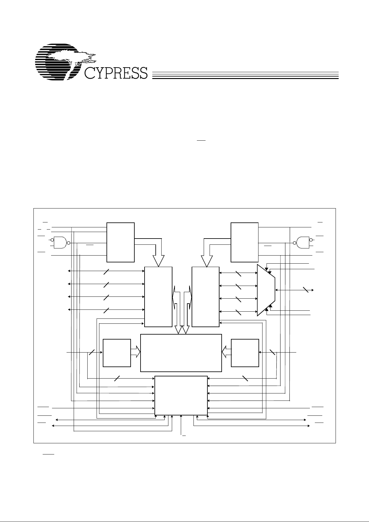
Logic Block Dia gram
A0L–A
13/14L
True Dual-Ported
RAM Array
BUSY
R
SEM
R
INT
R
Address
Decode
A
0R–A13/14R
[2]
[2]
[1] [1]
14/15 14/15
14/15 14/15
Left
Port
Control
Logic
I/O
18L
–I/O
26L
9
I/O
27L
–I/O
35L
9
I/O0L–I/O
8L
9
I/O9L–I/O
17L
9
Right
Port
Control
Logic
I/O
Control
9
9
I/O
R
9
9
Bus
Match
9/18/36
BA
BM
SIZE
WA
B
0–B3
For the most recent information, visit the Cypress web site at www.cypress.com

CY7C056V
CY7C057V
2
PRELIMINARY
Functional Description
The CY7C056V and CY7C057V are low-power CMOS 16K
and 32K x 36 dual-port static RAMs. Various arbitration
schemes are included on the devices to handle situations
when multipl e proces sor s access t he s ame piece of data. Tw o
ports are provided , pe rmitting i ndep endent, asyn chronous access for reads and writes to any location in memory. The devices can be utilized as standalone 36-bit dual-port static
RAMs or multip le devi ces can b e combined in o rder to fu nction
as a 7 2-bit o r wider master /sla v e d ual -port stati c RAM. An M/S
pin is prov ided f or impl ementi ng 72-bi t or wide r memory applications without the need for separate master and s lave devices or additional discrete logi c. Application areas include interprocessor/multiprocessor designs, communications status
buffering, and dual-port video/graphics memory.
Each port has independent control pins: Chip Enable (CE
)
[3]
,
Read or Write Enable (R/W
), and Output Enable (OE). Two
flags are provided on each port (BUSY
and INT). BUSY signals that the port is trying to access t he same location cur rently
being accessed b y the other port. TheInterrupt Flag (INT
) permits communicati on between ports or systems by means of a
mail box. The semaphores are used to pass a flag, or token,
from one port to the oth er to i ndicat e that a shared resource i s
in use. The semaphore logic is comprised of eight shared
latches. Only one side can control the latch (semaphore) at
any time. Control of a semaphore indicates that a shared resource is in use. An automatic Power-Down feature is controlled independently on each port by Chip Select (CE
0
and
CE
1
) pins.
The CY7C056V and CY7C057V are available in 144-Pin Thin
Quad Plastic Flatpack (TQFP) and 172-Ball Ball Grid Array
(BGA) packages.
Note:
3. CE
is LOW when CE0 ≤ VIL and CE1 ≥ VIH.

CY7C056V
CY7C057V
3
PRELIMINARY
Pin Configurations
Notes:
4. This pin is A14L for CY7C057V.
5. This pin is A14R for CY7C057V.
144-PinThin Quad Flatpack(TQFP)
Top View
I/O32L
I/O33R
I/O23L
I/O33L
2
3
4
I/O34L I/O34R
5
I/O35L I/O35R
6
A0L
A0R
7
A1L A1R
8
A2L
A2R
9
A3L
A3R
10
A4L
A4R
11
A5L
A5R
12
A6L
A6R
13
A7L
108
A7R
14
B0
107
BM
15
B1
106
SIZE
16
B2
105
WA
17
B3
104
BA
18
OEL
103
OER
19
R/WL
102
R/WR
20
VDD
101
VDD
21
VSS
100
VSS
22
VSS
99
VDD
23
CE0L
98
CE0R
24
CE1L
97
CE1R
25
M/S
96
VDD
26
SEML
95
SEMR
27
INTL
94
INTR
28
BUSYL
93
BUSYR
29
A8L
92
A8R
30
A9L
91
A9R
31
A10L
90
A10R
32
A11L
89
A11R
33
A12L
88
A12R
34
A13L
87
A13R
35
NC
86
NC
36
I/O26L
85
I/O26R
I/O25L
84
I/O25R
I/O24L
83
I/O24R
82
81
414243
44
I/O22L
I/O31L
45
VSS
VSS
46
I/O21L
I/O30L
47
I/O20L
I/O29L
48
I/O19L
I/O28L
49
I/O18L
I/O27L
50
VDD
VDD
51
I/O8L
I/O17L
52
I/O7L
I/O16L
53
I/O6L
I/O15L
54
I/O5L
I/O14L
55
VSS
VSS
56
I/O4L
I/O13L
57
I/O3L
I/O12L
58
I/O2L
143
I/O11L
59
I/O1L
142
I/O10L
60
I/O0L
141
I/O9L
61
I/O0R
140
I/O9R
62
I/O1R
139
I/O10R
63
I/O2R
138
I/O11R
64
I/O3R
137
I/O12R
65
I/O4R
136
I/O13R
66
VSS
135
VSS
67
I/O5R
134
I/O14R
68
I/O6R
133
I/O15R
69
I/O7R
132
I/O16R
70
I/O8R
131
I/O17R
71
VDD
130
VDD
72
I/O18R
129
I/O27R
123
I/O19R
128
I/O28R
122
I/O20R
127
I/O29R
121
I/O21R
126
I/O30R
120
VSS
125
VSS
119
I/O22R
124
I/O31R
118
I/O23R
I/O32R
117
116
373839
40
80
79
78
77
76
75
74
73
115
114
113
112
111
110
109
144
1
CY7C056V (16K x 36)
CY7C057V (32K x 36)
[4]
[5]
CY7C056V
CY7C057V
4
PRELIMINARY
Pin Configurations
(continued)
172-Ba ll B a ll G r id Ar ray (BG A )
T op View
1 23 4567891011121314
A
I/O32L I/O30L NC VSS I/O13L VDD I/O11L I/O11R VDD I/O13R VSS NC I/O30R I/O32R
B
A0L I/O33L I/O29 I/O17L I/O14L I/O12L I/O9L I/O9R I/O12R I/O14R I/O17R I/O29R I/O33R A0R
C
NC A1L I/O31L I/O27L NC I/O15L I/O10L I/O10R I/O15R NC I/O27R I/O31R A1R NC
D
A2L A3L I/O35L I/O34L I/O28L I/O16L VSS VSS I/O16R I/O28R I/O34R I/O35R A3R A2R
E
A4L A5L NC B0L NC NC NC NC BM NC A5R A4R
F
VDD A6L A7L B1L NC NC SIZE A7R A6R VDD
G
OEL B2L B3L CE0L CE0R BA WA OER
H
VSS R/WL A8L CE1L CE1R A8R R/WRVSS
J
A9L A10L VSS M/S NC NC VDD VDD A10R A9R
K
A11L A12L NC SEML NC NC NC NC SEMR NC A12R A11R
L
BUSYL A13L INTL I/O26L I/O25L I/O19L VSS VSS I/O19R I/O25R I/O26R INTR A13R BUSYR
M
NC NC I/O22L I/O18L NC I/O7L I/O2L I/O2R I/O7R NC I/O18R I/O22R NC NC
N
I/O24L I/O20L I/O8L I/O6L I/O5L I/O3L I/O0L I/O0R I/3R I/O5R I/O6R I/O8R I/O20R I/O24R
P
I/O23L I/O21L NC VSS I/O4L VDD I/O1L I/O1R VDD I/O4R VSS NC I/O21R I/O23R
[5]
[4]
CY7C056V
CY7C057V
5
PRELIMINARY
Maximum Ratings
(Above which the useful life m ay be impaired. F or user guidelines, not tested.)
Storage Tem perature ........................... .. ....–65
°
C to +150°C
Ambient Temperature with
Power Applied.............................................–55
°
C to +125°C
Supply Voltage to Ground Potential............... –0.5V to +4.6V
DC V oltage Applied to
Outputs in High Z State ...........................–0.5V to V
DD
+0.5V
DC Input Voltage...................................–0. 5V to V
DD
+0.5V
[6]
Output Current into Outputs (LOW)............................. 20 mA
Static Discharge Voltage.................... ...................... >2001V
Latch-Up Current............. .. .............. ....................... >200 mA
Shaded areas contain advance information.
Note:
6. Pulse width < 20 ns.
Selectio n Guide
CY7C056V
CY7C057V
-10
CY7C056V
CY7C057V
-12
CY7C056V
CY7C057V
-15
CY7C056V
CY7C057V
-20
Maximum Access Time (ns) 10 12 15 20
Typical Operat ing Current (mA) 260 250 240 230
Typical Standb y Current for I
SB1
(mA) (Both Ports TTL Level) 60 55 50 45
Typical Standb y Current for I
SB3
(µA) (Both Ports CMOS
Level)
10 µA10 µA 10 µA 10 µA
Pin Definitions
Left Port Right Port Description
A0L–A
13/14L
A0R–A
13/14R
Address (A0–A13 for 16K ; A0–A14 for 32K devices)
SEML SEM
R
Semaphore Enable
CE0L, CE
1L
CE0R, CE
1R
Chip Enable (CE is LOW when CE0 ≤ VIL and CE1 ≥ VIH)
INT
L
INT
R
Interrupt Flag
BUSY
L
BUSY
R
Busy Flag
I/O0L–I/O
35L
I/O0R–I/O
35R
Data Bus Input/Output
OE
L
OE
R
Output Enable
R/W
L
R/W
R
Read/Write Enable
B0–B
3
Byte Select Inputs. Asserting these signals enables read and write oper-
ations to the corresponding bytes of the memory array.
BM, SIZE See Bus Matching for detai ls.
WA, B A See Bus Matching for detai ls.
M/S Master or Slave Select
V
SS
Ground
V
DD
Power
Operating Range
Range
Ambient
Temperature
V
DD
Commercial 0°C to +70°C 3.3V ± 165 mV
Industrial –40°C to +85°C 3.3V ± 165 mV
CY7C056V
CY7C057V
6
PRELIMINARY
Shaded areas contain advance information.
Notes:
7. Cross Levels are V
DD
– 0.2V< VZ<0.2V.
8. Deselection for a port occurs if CE
0
is HIGH or if CE1 is LOW.
9. f
MAX
= 1/tRC = All inputs cycling at f = 1/tRC (except Output Enable). f = 0 means no address or control lines change. This applies only to inputs at CMOS level
standby I
SB3
.
10. Tested initially and after any design or process changes that may affect these parameters.
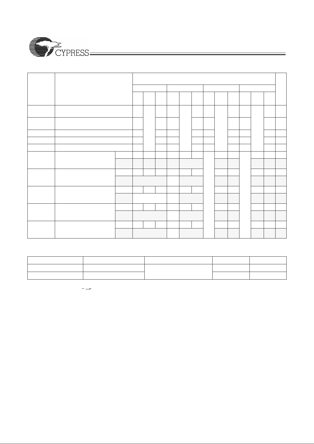
Electrical Characteristics
Over the Operating Range
[7, 8]
Parameter Description
CY7C056V
CY7C057V
Unit
-10 -12 -15 -20
Min.
Typ.
Max.
Min.
Typ.
Max.
Min.
Typ.
Max.
Min.
Typ.
Max.
V
OH
Output HIGH Voltage
(V
DD
= Min. , I
OH
= –4.0 mA) 2.4 2.4 2.4 2.4 V
V
OL
Output LO W Voltage
(V
DD
= Min. , I
OL
= +4.0 mA) 0.4 0.4 0.4 0.4 V
V
IH
Input HIGH Voltage 2.0 2.0 2.0 2.0 V
V
IL
Input LOW Voltage 0.8 0.8 0.8 0.8 V
I
OZ
Output Leakage Curr ent -10 10 –10 10 –10 10 –10 10 µA
I
CC
Operating Cur rent (V
DD
=
Max., I
OUT
= 0 mA) Outputs
Disabled
Com’l. 260 410 250 385 240 360 230 340 mA
Indust.
265 385 mA
I
SB1
Standby Cur rent (Both P orts
TTL Lev el and Deselected)
f = f
MAX
Com’l. 60 80 55 75 50 70 45 65 mA
Indust.
65 95 mA
I
SB2
Standby Current (One Port
TTL Lev el and Deselected)
f = f
MAX
Com’l. 185 250 180 240 175 230 165 210 mA
Indust.
190 255 mA
I
SB3
Standby Cur rent (Both P orts
CMOS Level and Deselected) f =0
Com’l. 0.01 1 0.01 1 0.01 1 0.01 1 mA
Indust.
0.01 1 mA
I
SB4
Standby Current (One Port
CMOS Level and Deselected) f = f
MAX
[9]
Com’l. 170 220 160 210 155 200 145 180 mA
Indust.
170 215 mA
Capacitance
[10]
Parameter Description Test Conditions Max. Unit
C
IN
Input Capacitance TA = 25°C, f = 1 MHz,
V
DD
= 3.3V
10 pF
C
OUT
Output Capacitance 10 pF
CY7C056V
CY7C057V
7
PRELIMINARY
Notes:
11. External AC Test Load Capacitance = 10 pF.
12. (Internal I/O pad Capacitance = 10 pF) + AC Test Load.
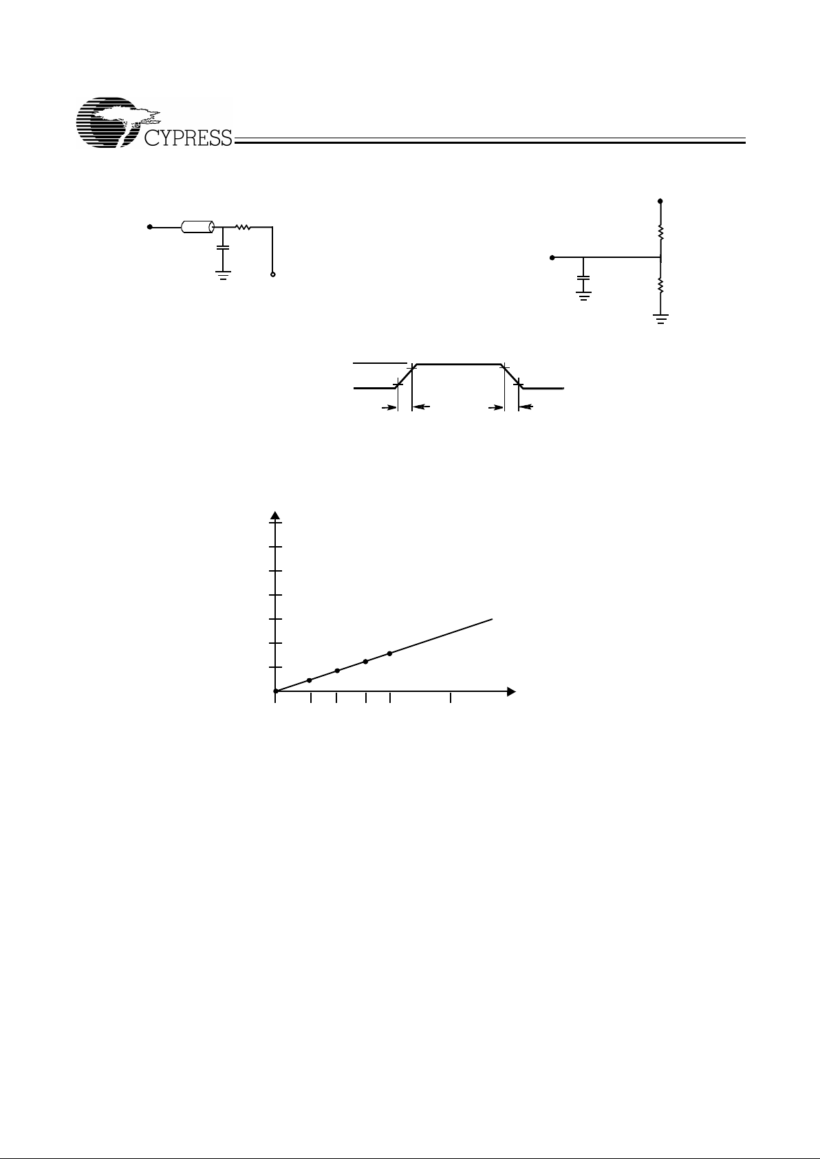
AC Test Load and Waveforms
VTH=1.5V
OUTPUT
C
(a) Normal Load (Load 1)
R = 50
Ω
Z0 = 50
Ω
[11]
3.0V
V
SS
90%
90%
10%
3ns
3
ns
10%
≤
≤
ALL INPUT PULSES
3.3V
OUTPUT
C = 5 pF
(b) Three-State Delay (Load 2)
R2 = 435
Ω
R1 = 590
Ω
(b) Load Derating Curve
1
2
3
4
5
6
7
30 60 80 100 200
∆
(ns) for access time
Capacitance (pF)
20
[12]
 Loading...