

Datasheet CY7C038-20AI, CY7C038-20AC, CY7C038-15AI, CY7C028-20AI, CY7C028-20AC Datasheet (Cypress Semiconductor)
...
PRELIMINARY
32K/64K x 16/18
Dual-Port Static RAM
CY7C027/028
CY7C037/038
Cypress Semiconductor Corporation
• 3901 North First Street • San Jose • CA 95134 • 408-943-2600
November 23
,
1998
5
1
Features
• T rue Dual-Ported memory cells which allow si m ultaneous access of the same memory locat ion
• 32K x 16 organization (CY7C027)
• 64K x 16 organization (CY7C028)
• 32K x 18 organization (CY7C037)
• 64K x 18 organization (CY7C038)
• 0.35-micron CMOS for optimum speed/power
• High-speed access: 12
[1]
/15/20 ns
• Low operat i n g power
—
Active: I
CC
= 180 mA (typical)
—Standby: I
SB3
= 0.05 mA (typical)
• Fully asynchronous operation
• Automatic power-down
• Expandabl e data bus to 32/36 bits or more using Master/Slave chip sel ect when using more than one device
• On-chip arbitration logic
• Semaphores inc luded to permit software handshak ing
between ports
•INT flags f or port-to-port communication
• Separate upper-byte and lower-byte cont rol
• Dual Chip Enables
• Pin select for Master or Slave
• Commercial and industrial temperature ranges
• Available in 100-pin TQFP
• Pin-compatible and functionally equivalent to IDT7027
Notes:
1. See page 6 for Load Conditions.
2. I/O
8
–I/O15 for x16 devices; I/O9–I/O17 for x18 devices.
3. I/O
0
–I/O7 for x16 devices; I/O0–I/O8 for x18 dev ices.
4. A
0–A14
for 32K; A0–A15 for 64K devices.
5. BUSY
is an output in master mode and an input in slave mode.
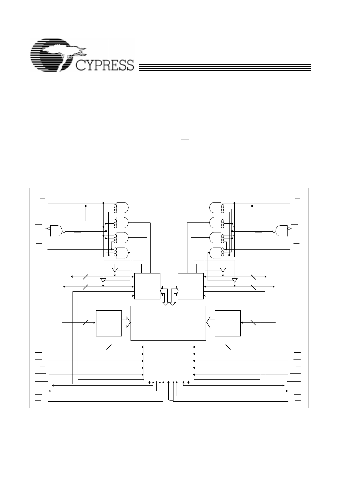
R/W
L
CE
0L
CE
1L
OE
L
I/O
8/9L
–I/O
15/17L
I/O
Control
Address
Decode
A
0L–A14/15L
CE
L
OE
L
R/W
L
BUSY
L
I/O
Control
CE
L
Interrupt
Semaphore
Arbitration
SEM
L
INT
L
M/S
UB
L
LB
L
I/O0L–I/O
7/8L
R/W
R
CE
0R
CE
1R
OE
R
I/O
8/9L
–I/O
15/17R
CE
R
UB
R
LB
R
I/O0L–I/O
7/8R
UB
L
LB
L
Logic Block Diagram
A0L–A
14/15L
True Dual-Ported
RAM Array
A0R–A
14/15R
CE
R
OE
R
R/W
R
BUSY
R
SEM
R
INT
R
UB
R
LB
R
Address
Decode
A
0R–A14/15R
[2]
[2]
[3]
[3]
[4]
[4]
[5]
[5]
[4] [4]
15/16
8/9
8/9
15/16
8/9
8/9
15/16 15/16
For the most recent information, visit the Cypress web site at www.cypress.com
CY7C027/028
CY7C037/038
PRELIMINARY
2
Functional Description
The CY7C027/028 and CY7C037/038 are low-power CMOS
32K, 64K x 16/18 dual-port static RAMs. Various arbitration
schemes are included on the devices to handle situations
when multipl e proces sors acc ess t he sam e piece of data. Two
ports are provided , pe rmitting i ndep endent, asynchr onous access for reads and writes to any location in m emory. The devices can be utilized as standalone 16/18-bit dual-port static
RAMs or multip le devi ces can b e combined in o rder to funct ion
as a 32/36-bit or wider master/slave dual-port static RAM. An
M/S
pin is provided for implementing 32/36-bit or wider memory applications without the need for separate master and
slave devices or additional discrete logic. Application areas
include interprocessor/multiprocessor designs, communications status buffering, and dual-port video/graphics memory.
Each port has independent control pins: dual chip enables
(CE
0
and CE1), read or write enable (R/W), and output enable
(OE
). Two flags are provided on each port (BUSY and INT). BUSY
signals that the port is tryi ng to access the same location currently
being accessed by the ot her port. Th e interrupt flag (INT
) permits
communication between ports or systems by means of a mail box.
The semaphores are used to pass a flag, or token, from one port to
the other to indicate that a shared resource is in use. The semaphore
logic is comprised of eight shared latches. Only one side can control
the latch (semaphore) at any time. Control of a semaphore indicates
that a shared resource is in use. An automatic power-down feature is
controlled independently on each port by the chip enable pins.
The CY7C027/028 and CY7C03 7/0 38 are a v ail abl e in 100 -pin
Thin Quad Plastic Flatpack (TQFP) packages.
Pin Configurations
100- Pin TQ FP (Top View)
Note:
6. This pin is NC for CY7C027.
1
3
2
92 91 90 848587 868889 83 82 81 7678 77798093949596979899100
59
60
61
67
66
64
65
63
62
68
69
70
75
73
74
72
71
A9R
A10R
A11R
A12R
A13R
A14R
UBR
NC
LBR
CE1R
SEMR
OER
GND
NC
A15R
GND
R/WR
GND
I/O15R
I/O14R
I/O13R
I/O12R
I/O11R
I/O10R
CE0R
58
57
56
55
54
53
52
51
CY7C02 7 (32K x 16)
A9L
A10L
A11L
A12L
A13L
A14L
UBL
NC
LBL
CE1L
SEML
OEL
GND
NC
A15L
VCC
R/WL
GND
I/O15L
I/O14L
I/O13L
I/O12L
I/O11L
I/O10L
CE0L
17
16
15
9
10
12
11
13
14
8
7
6
4
5
18
19
20
21
22
23
24
25
A8L
A7L
A6L
A5L
A4L
A3L
INTL
A1L
NC
GND
M/S
A0R
A1R
A0L
A2L
BUSYR
INTR
A2R
A3R
A4R
A5R
A6R
A7R
A8R
BUSYL
34 35 36 424139 403837 43 44 45 5048 494746
NC
I/O9R
I/O8R
I/O7R
VCC
I/O6R
I/01R
I/O4R
I/O2R
GND
I/O0L
I/O2L
I/O3L
I/O3R
I/O5R
I/O1L
GND
I/O4L
I/O5L
I/O6L
I/O7L
VCC
I/O8L
I/O9L
I/O0R
3332313029282726
CY7C02 8 (64K x 16)
[Note 6]
[Note 6]
CY7C027/028
CY7C037/038
PRELIMINARY
3
Pin Configurations
(continued)
100- Pin TQ FP (Top View)
Note:
7. This pin is NC for CY7C037.
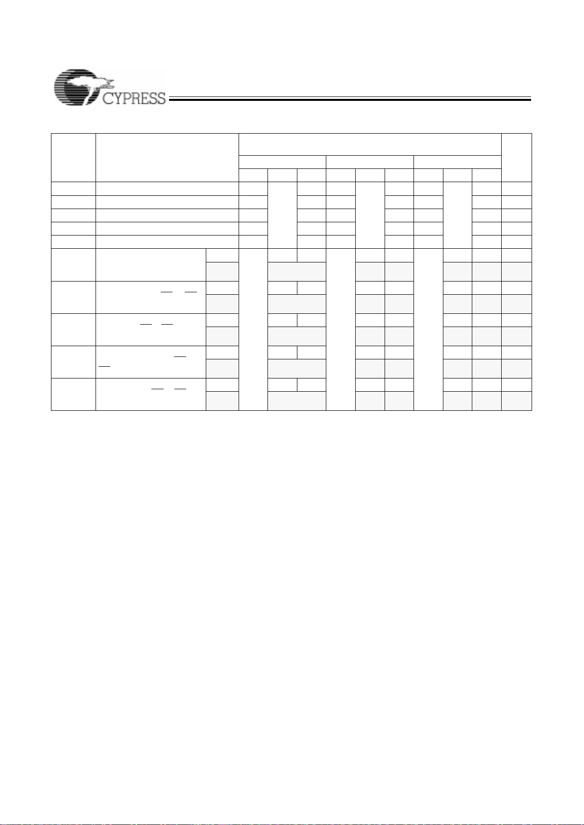
Selection Guide
CY7C027/028
CY7C037/038
-12
[1]
CY7C027/028
CY7C037/038
-15
CY7C027/028
CY7C037/038
-20
Maximum Access Time (ns) 12 15 20
Typical Operating Current (mA) 195 190 180
Typical Standby Current for I
SB1
(mA) (Both ports TTL lev el) 55 50 45
Typical Standby Curren t for I
SB3
(mA) (Both ports CMOS level) 0.05 0.05 0.05
1
3
2
92 91 90 848587 868889 83 82 81 7678 77798093949596979899100
59
60
61
67
66
64
65
63
62
68
69
70
75
73
74
72
71
A8R
A9R
A10R
A11R
A12R
A13R
CE0R
A15R
UBR
SEMR
R/WR
GND
I/O17R
LBR
A14R
GND
OER
GND
I/O16R
I/O15R
I/O14R
I/O13R
I/O12R
I/O11R
CE1R
58
57
56
55
54
53
52
51
CY7C03 7 (32K x 18)
A9L
A10L
A11L
A12L
A13L
A14L
CE1L
LBL
CE0L
R/WL
OEL
I/O17L
I/O16L
UBL
A15L
VCC
GND
GND
I/O15L
I/O14L
I/O13L
I/O12L
I/O11L
I/O10L
SEML
17
16
15
9
10
12
11
13
14
8
7
6
4
5
18
19
20
21
22
23
24
25
A8L
A7L
A6L
A5L
A4L
A3L
BUSYL
A1L
INTL
GND
VCC
INTR
A0R
A0L
A2L
M/S
BUSYR
A1R
A2R
A3R
A4R
A5R
A6R
A7R
GND
34 35 36 424139 403837 43 44 45 5048 494746
I/O10R
I/O9R
I/O8R
I/O7R
VCC
I/O6R
I/01R
I/O4R
I/O2R
GND
I/O0L
I/O2L
I/O3L
I/O3R
I/O5R
I/O1L
GND
I/O4L
I/O5L
I/O6L
I/O7L
VCC
I/O8L
I/O9L
I/O0R
3332313029282726
CY7C03 8 (64K x 18)
[Note 7]
[Note 7]
CY7C027/028
CY7C037/038
PRELIMINARY
4
Maximum Ratings
(Above which the useful life may be impaired. For user guidelines, not tested.)
Storage Temperat ure ............ ................. ....–65
°
C to +150°C
Ambient Temperature wit h
Power Applied.............................................–55
°
C to +125°C
Supply Voltage to Ground Potential...............–0. 3V to +7.0V
DC V oltage Applied to Outputs
in High Z State............................................ –0.5V to +7.0DC
Input Voltage
[8]
............................................... –0.5V to +7.0V
Output Current into Outputs (LOW)............................. 20 mA
Static Discharge Voltage ....................... ................... >1100V
Latch-Up Current............................. ................. ...... >200 mA
Note:
8. Pulse width < 20 ns.
Pin Definitions
Left Port Right Port Description
CE0L, CE
1L
CE0R, CE
1R
Chip Enable (CE is LOW when CE0 ≤ VIL and CE1 ≥ VIH)
R/W
L
R/W
R
Read/Write Enable
OE
L
OE
R
Output Enable
A0L–A
15L
A0R–A
15R
Address (A0–A14 for 32K ; A0–A15 for 64K devices)
I/O0L–I/O
17L
I/O0R–I/O
17R
Data Bus Input/Output (I/O0–I/O15 for x16 devices; I/O0–I/O17 for x18)
SEML SEM
R
Semaphore Enable
UB
L
UB
R
Upper Byte Select (I/ O8–I/O15 for x1 6 de v ices; I/O9–I/O17 for x18 devi ces)
LB
L
LB
R
Lower Byte Select (I/ O0–I/O7 for x16 devices; I/O0–I/O8 for x18 devices)
INT
L
INT
R
Interrupt Flag
BUSY
L
BUSY
R
Busy Flag
M/S Master or Slave Select
V
CC
Power
GND Ground
NC No Connect
Operating Range
Range
Ambient
Temperature
V
CC
Commercial 0°C to +70°C 5V ± 10%
Industrial –40°C to +85°C 5V ± 10%
Shaded area contains advance information.
CY7C027/028
CY7C037/038
PRELIMINARY
5
Shaded area contains advance information.
Note:
9. f
MAX
= 1/tRC = All inputs c ycling at f = 1/tRC (except output enab le) . f = 0 mea ns no add ress or contr ol li nes change . T his appl ies only to i nputs at C MOS le v el s tandb y I
SB3
.
Electrical Characteristics
Over the Ope rating Range
Symbol Parameter
CY7C027/028
CY7C037/038
Units
-12
[1]
-15 -20
Min Typ Max Min Typ Max Min Typ Max
V
OH
Output HIGH Voltage (VCC=5V) 2.4 2.4 2.4 V
V
OL
Output LOW Voltage 0.4 0.4 0.4 V
V
IH
Input HIGH Voltage 2. 2 2.2 2.2 V
V
IL
Input LOW Voltage 0.8 0.8 0.8 V
I
OZ
Output Leakage Current –10 10 –10 10 –10 10 µA
I
CC
Operating Curr ent
(V
CC
=Max, I
OUT
=0 mA)
Outputs Disabled
Com’l. 195 325 190 280 180 265 mA
Indust. 215 305 305 290 mA
I
SB1
Standby Current (Both
Ports TTL Le vel) CE
L
& CER
≥ V
IH
, f=f
MAX
Com’l. 55 75 50 70 45 65 mA
Indust. 65 95 60 80 mA
I
SB2
Standby Current (One Port
TTL Lev el) CE
L
| CER ≥ VIH,
f=f
MAX
Com’l. 125 205 120 180 110 160 mA
Indust. 135 205 125 175 mA
I
SB3
Standby Current (Both
Ports CMOS Level) CE
L
&
CE
R
≥ V
CC
– 0.2V, f=0
Com’l. 0.05 0.25 0.05 0.25 0.05 0.25 mA
Indust. 0.05 0.25 0.05 0.25 mA
I
SB4
Standby Current (One Port
CMOS Level) CE
L
| CER ≥
V
IH
, f=f
MAX
[9]
Com’l. 115 185 110 160 100 140 mA
Indust. 125 175 115 155 mA
CY7C027/028
CY7C037/038
PRELIMINARY
6
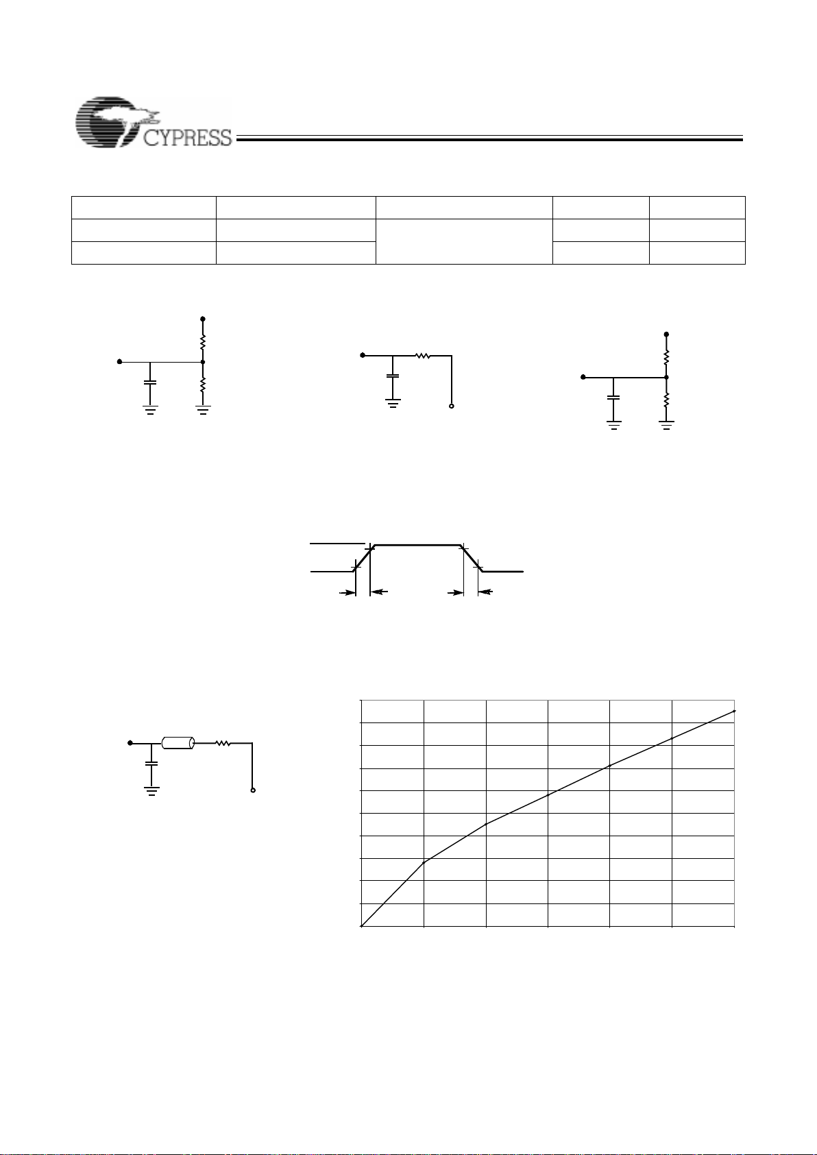
AC Test Loads (Applicable to -12 only)
[11]
Notes:
10. Tested initially and after any design or process changes that may affect these parameters.
11. Test Conditions: C = 0 pF.
Capacitance
[10]
Parameter Description Test Conditions Max. Unit
C
IN
Input Capacitance TA = 25°C, f = 1 MHz,
V
CC
= 5.0V
10 pF
C
OUT
Output Capacitance 10 pF
AC Test Loads and Waveforms
3.0V
GND
90%
90%
10%
3ns
3
ns
10%
ALL INPUT PULSES
(a) Normal Load( Load 1)
R1= 893
Ω
5V
OUTPUT
R2= 347
Ω
C= 30
pF
V
TH
=1.4V
OUTPUT
C=
30 pF
(b) Thévenin Equivalent (Load 1)
(c)Three-State Delay(Load 2)
R1= 893
Ω
R2= 347
Ω
5V
OUTPUT
C= 5pF
R
TH
=250
Ω
≤
≤
(Used for t
CKLZ
, t
OLZ
, & t
OHZ
including scope and jig)
VTH=1.4V
OUTPUT
C
(a) Load 1 (-12 only)
R = 50
Ω
(b) Load Derating Curve
Capacitance
(pF)
∆
(ns) for al l -12 access times
0.00
0.10
0.20
0.30
0.40
0.50
0.60
0.70
0.80
0.90
1.00
0 5 10 15 20 25 30
Z0 = 50
Ω

CY7C027/028
CY7C037/038
PRELIMINARY
7
Switching Characteristics
Over the Operating Range
[12]
Parameter Description
CY7C027/028
CY7C037/038
Unit
–12
[1]
–15 –20
Min. Max. Min. Max. Min. Max.
READ CYCLE
t
RC
Read Cycle Time 12 15 20 ns
t
AA
Address to Data Valid 12 15 20 ns
t
OHA
Output Hold From Address Change 3 3 3 ns
t
ACE
[13]
CE LOW to Data Valid 12 15 20 ns
t
DOE
OE LOW to Data Valid 8 10 12 ns
t
LZOE
[14, 15, 16]
OE LOW to Low Z 3 3 3 ns
t
HZOE
[14, 15, 16]
OE HIGH to High Z 10 10 12 ns
t
LZCE
[14, 15, 16]
CE LOW to Low Z 3 3 3 ns
t
HZCE
[14, 15, 16]
CE HIGH to High Z 10 10 12 ns
t
PU
[16]
CE LOW to Power-Up 0 0 0 ns
t
PD
[16]
CE HIGH to Power-Down 12 15 20 ns
t
ABE
[13]
Byte Enable Access Time 12 15 20 ns
WRITE CYCLE
t
WC
Wri te Cycl e Time 12 15 20 ns
t
SCE
[13]
CE LOW to Write End 10 12 15 ns
t
AW
Address Valid to Write End 10 12 15 ns
t
HA
Address Hold From Write End 0 0 0 ns
t
SA
[13]
Address Set-Up to Write Start 0 0 0 ns
t
PWE
Writ e Pu ls e Wid t h 10 12 15 ns
t
SD
Data Se t- U p to Wr ite End 10 10 15 ns
t
HD
Data Hold From Write End 0 0 0 ns
t
HZWE
[15, 16]
R/W LO W to High Z 10 10 12 ns
t
LZWE
[15, 16]
R/W HI GH to Low Z 3 3 3 ns
t
WDD
[17]
Write Pulse to Data Delay 25 30 45 ns
t
DDD
[17]
Write Data Valid to Read Data Valid 20 25 30 ns
Notes:
12. Tes t conditions assume signal transition time of 3 ns or less, timing reference levels of 1.5V , input pulse levels of 0 to 3.0V, and output loading of the specified
I
OI/IOH
and 30-pF load capac itance.
13. To access RAM, CE
=L, UB=L, SEM= H. To access semaph ore , CE=H and S EM=L. Either conditi on mu st be v al id f or the entir e t
SCE
time.
14. At any given temperature and voltage condition for any given device, t
HZCE
is less than t
LZCE
and t
HZOE
is less than t
LZOE
.
15. Test conditions used are Load 2.
16. This parameter is guaranteed by design, but it is not production tested.
17. For information on port-to-port delay through RAM cells from writing port to reading port, refer to Read Timing with Busy waveform.

CY7C027/028
CY7C037/038
PRELIMINARY
8
Data Retention Mode
The CY7C027/028 and CY7C037/038 are designed with battery backup in m ind. Data retent ion voltage and suppl y curr ent
are guaranteed over temperature. The following rules ensure
data retention:
1. Chip enabl e (CE
) must be held HIGH during data retention, with-
in V
CC
to VCC – 0.2V.
2. CE
must be kept between VCC – 0.2V and 70% of VCC
during the power-up and power-down transitions.
3. The RAM can begin operati on >t
RC
after VCC reaches the
minimum operating voltage (4.5 volts).
BUSY TIMING
[18]
t
BLA
BUSY LOW from Address Match 12 15 20 ns
t
BHA
BUSY HIGH from Address Mismatch 12 15 20 ns
t
BLC
BUSY LOW from CE LOW 12 15 20 ns
t
BHC
BUSY HIGH from CE HIGH 12 15 17 ns
t
PS
Port Set-Up for Priority 5 5 5 ns
t
WB
R/W HIGH after BUSY (Slave) 0 0 0 ns
t
WH
R/W HIGH after BUSY HIGH (Slave) 11 13 15 ns
t
BDD
[19]
BUSY HIGH to Data Valid 12 15 20 ns
INTERRUPT TIMING
[18]
t
INS
INT Set Time 12 15 20 ns
t
INR
INT Reset Time 12 15 20 ns
SEMAPHORE TIMING
t
SOP
SEM Flag Update Pulse (OE or SEM) 10 10 10 ns
t
SWRD
SEM Flag Write to Read Time 5 5 5 ns
t
SPS
SEM Flag Contention Window 5 5 5 ns
t
SAA
SEM Address Access Time 12 15 20 ns
Switching Characteristics
Over the Operating Range
[12]
(continued)
Parameter Description
CY7C027/028
CY7C037/038
Unit
–12
[1]
–15 –20
Min. Max. Min. Max. Mi n. Max.
Timing
Parameter Test Conditions
[20]
Max. Unit
ICC
DR1
@ VCCDR = 2V 1.5 mA
Data Retention Mode
4.5V
4.5V
V
CC
>
2.0V
V
CC
to VCC– 0.2V
V
CC
CE
t
RC
V
IH
Notes:
18. Test conditions used are Load 1.
19. t
BDD
is a calculated pa rameter and is t he gr eater o f t
WDD–tPWE
(actu al ) o r t
DDD–tSD
(actu al ).
20. CE
= VCC, Vin = GND to VCC, TA = 25°C. This parameter is guaranteed but not tested.

CY7C027/028
CY7C037/038
PRELIMINARY
9
Switching Waveforms
Notes:
21. R/W
is HIGH for read cycles.
22. Device is continuously selected CE = VIL and UB or LB = VIL. This wav ef orm cannot be used f or se maphore r eads.
23. OE
= VIL.
24. Address valid prior to or coincident with CE
transition LO W.
25. To access RAM, CE
= VIL, UB or LB = VIL, SEM = VIH. T o ac cess semaphore, CE = VIH, SEM = VIL.
t
RC
t
AA
t
OHA
DATA VA LI DPREVIOUS DATA VALID
DATA OU T
ADDRESS
t
OHA
Read Cycle No. 1 (Either P ort Address Access)
[21,22,2 3]
t
ACE
t
LZOE
t
DOE
t
HZOE
t
HZCE
DATA VALID
t
LZCE
t
PU
t
PD
I
SB
I
CC
DATA OUT
OE
CE and
LB
or UB
CURRENT
Read Cycle No. 2 (Eithe r Port CE/OE Access)
[21,24,25]
UB or LB
DAT A OUT
t
RC
ADDRESS
t
AA
t
OHA
CE
t
LZCE
t
ABE
t
HZCE
t
HZCE
t
ACE
t
LZCE
Read Cycle No. 3 (Eithe r Port)
[21,23,2 4,25]

CY7C027/028
CY7C037/038
PRELIMINARY
10
Notes:
26. R/W
must be HIGH during all addr ess transi tions.
27. A write occurs during the overlap (t
SCE
or t
PWE
) of a LO W CE or SEM and a LO W UB or LB.
28. t
HA
is measured from the ea rlier of CE or R /W or (SEM or R/W) going HIGH at t he end of wr ite cycle .
29. If OE
is LOW during a R/W controlled write cy cle, the write pulse widt h must be the larger of t
PWE
or (t
HZWE
+ tSD) to allow the I/O driver s to turn off and data to be placed on
the bus for the required t
SD
. If OE is HI GH during an R/W controlled write cyc le, this re quireme nt doe s not app ly and the write p ulse can be as s hort as the s pecifi ed t
PWE
.
30. To access RAM, CE
= VIL, SEM = VIH.
31. To access upper byte, CE
= VIL, UB = VIL, SEM = VIH.
To acce ss l ower by t e , C E
= VIL, LB = VIL, SEM = VIH.
32. Transition is measured ±500 mV from steady state with a 5- pF loa d (includi ng scope and ji g). T his par ameter i s sampl ed and not 100% tested.
33. During this period, the I/O pins are in the output state, and input signals must not be applied.
34. If the CE
or SEM LOW transi tion occ urs simu lt aneously with o r after the R/W LO W tr ansi tion, the out puts remai n in t he high- impedance sta te.
Switching Waveforms
(continued )
t
AW
t
WC
t
PWE
t
HD
t
SD
t
HA
CE
R/W
OE
DA TA OUT
DATA IN
ADDRESS
t
HZOE
t
SA
t
HZWE
t
LZWE
Write Cycle No. 1: R/W Controlled Timing
[26,27,28,29]
[32]
[32]
[29]
[30,31]
NOTE 33
NOTE 33
t
AW
t
WC
t
SCE
t
HD
t
SD
t
HA
CE
R/W
DATA IN
ADDRESS
t
SA
Write Cycle No. 2: CE Control led Timing
[26,27,2 8,34]
[30,31]

CY7C027/028
CY7C037/038
PRELIMINARY
11
Notes:
35. CE
= HIGH for the duration of the above timing (both write and read cycle).
36. I/O0R = I/O0L = LOW (reques t semaph ore); CER = CEL = HIGH.
37. Semaphores are reset (available to both ports) at cycle start.
38. If t
SPS
is violated, the s emaphore w ill de finitel y be obt ained b y one s ide or the ot her, but which side will get the semaphore is unpredictable.
Switching Waveforms
(continued )
t
SOP
t
SAA
VALID ADRESS VA LID ADRESS
t
HD
DAT AINVALID
DA TA
OUT
VALID
t
OHA
t
AW
t
HA
t
ACE
t
SOP
t
SCE
t
SD
t
SA
t
PWE
t
SWRD
t
DOE
WRITE CYCLE READ CYCLE
OE
R/W
I/O
0
SEM
A0–A
2
Semaphore Read After Write Timing, Either Side
[35]
MATCH
t
SPS
A0L–A
2L
MATCH
R/W
L
SEM
L
A0R–A
2R
R/W
R
SEM
R
Timing Diagram of Semaphore Contention
[36,37,38]

CY7C027/028
CY7C037/038
PRELIMINARY
12
Note:
39. CE
L
= CER = LOW.
Switching Waveforms
(continued )
VALID
t
DDD
t
WDD
MATCH
MATCH
R/W
R
DATA IN
R
DAT A
OUTL
t
WC
ADDRESS
R
t
PWE
VALID
t
SD
t
HD
ADDRESS
L
t
PS
t
BLA
t
BHA
t
BDD
BUSY
L
Timing Diagram of Read with BUSY (M/S=HIGH)
[39]
t
PWE
R/W
BUSY
t
WB
t
WH
Write Timing with Busy Input (M/S=LOW)

CY7C027/028
CY7C037/038
PRELIMINARY
13
Note:
40. If t
PS
is violated, the b us y s ignal will be asserted on one side or the other , b ut t her e is no guar a ntee t o which s ide BU SY will be asserted.
Switching Waveforms
(continued )
ADDRESS MA TCH
t
PS
t
BLC
t
BHC
ADDRESS MA TCH
t
PS
t
BLC
t
BHC
CERValid First:
ADDRESS
L,R
BUSY
R
CE
L
CE
R
BUSY
L
CE
R
CE
L
ADDRESS
L,R
Busy Timing Diagram No.1 (CE Arbitration)
[40]
CELVal id First :
ADDRESS MA TCH
t
PS
ADDRESS
L
BUSY
R
ADDRESS MISMATCH
t
RC
or t
WC
t
BLA
t
BHA
ADDRESS
R
ADDRESS MA TCH ADDRESS MISMATCH
t
PS
ADDRESS
L
BUSY
L
tRCor t
WC
t
BLA
t
BHA
ADDRESS
R
Right AddressValid First:
Busy Timing Diagram No. 2 (Address Arbitration)
[40]
Left Address Valid First:

CY7C027/028
CY7C037/038
PRELIMINARY
14
Notes:
41. t
HA
depends on which enab l e pin (CEL or R/WL) is deasserted first.
42. t
INS
or t
INR
depends on which enabl e p in (CEL or R/WL) is asserted last.
Switching Waveforms
(continued )
Interrupt Timing Diagrams
WRITE 7FFF (FFFF for CY7C028/38)
t
WC
Right SideClears INTR:
t
HA
READ 7FFF
t
RC
t
INR
WRITE 7FFE (FFFE for CY7C028/38)
t
WC
Right SideSets INT
L
:
Left Side Sets INT
R
:
Left SideClears INTL:
READ 7FFE
t
INR
t
RC
ADDRESS
R
CE
L
R/W
L
INT
L
OE
L
ADDRESS
R
R/W
R
CE
R
INT
L
ADDRESS
R
CE
R
R/W
R
INT
R
OE
R
ADDRESS
L
R/W
L
CE
L
INT
R
t
INS
t
HA
t
INS
(FFFF for CY7C028/38)
(FFFE for CY7C028/38)
[41]
[42]
[42]
[42]
[41]
[42]

CY7C027/028
CY7C037/038
PRELIMINARY
15
Architecture
The CY7C027/028 and CY7C037/038 consist of an array of
32K and 64K words of 16 and 18 bits each of dual-port RAM
cells, I/ O and add ress li nes, and c ontrol signal s (CE
, OE, R/W).
These control pins permit independent access for reads or writes to
any location in memory. To handle simultaneous writes/reads to the
same location, a BUSY
pin is provided on each port. Two interrupt
(INT
) pins can be utilized f or port-to-port communication. Two sema-
phore (SEM
) control pins are used for allocating sh are d resources.
With the M/S
pin, the devices can function as a master (BUSY pi ns
are outputs) or as a slave (BUSY
pins are inputs). The devices also
have an automatic power-down feature controlled by CE
. Each port
is provided with its own output enable control (OE
), which allows data
to be read from the device.
Functional Description
Write Operation
Data must be set up for a duration of t
SD
before the rising edge
of R/W
in order to guarantee a valid write. A write operation is con-
trolled by either the R/W
pin (see Write Cycle No. 1 wavef orm) or the
CE
pin (see Write Cycle No. 2 waveform). Required inputs for
non-contention operations are summarized in
Table 1
.
If a location is being written to by one port and the opposite
port attempts to read that location, a port-to-port flowthrough
delay m ust occur before the data is read on the output; otherwise the data read is not deterministi c. Data will be va lid on the
port t
DDD
after the data is presented on the other port.
Read Operation
When reading the device, the user must assert both the OE
and CE pins. Data will be available t
ACE
after CE or t
DOE
after OE is
asserted. If the user w ishes to access a semaph ore flag, then the
SEM
pin must be asserted instead of the CE pin, and OE must also
be asserted.
Interrupts
The upper two memory locations may be used for message
passing. The highest memory location (7FFF for the
CY7C027/37, FFFF f or the CY7C028/38) is the mail box f or the
right port and the second-highest memory location (7FFE for
the CY7C027/37, FFFE for the CY7C028/38) is the mailb ox f or
the left port. When one port writes t o the other port’s mailbox,
an interrupt is generated to the owner. The interrupt is reset
when the owner reads the contents of the mailbox. The message is user defined.
Each port can read the other port’s mailbox without resetting
the interrupt. The active state of the busy signal (to a port)
preve nts the port from sett ing th e inter rupt to t he winni ng port.
Also, an active busy to a port prevents that port from reading
its own mailbox and, thus, resetting the interrupt to it.
If an application does not require message passing, do not
connect the interrupt pin to the processor’s interrupt request
input pin.
The operation of the interrupts and their interaction with Busy
is summarized in
Table 2.
Busy
The CY7C027/028 an d CY7C03 7/038 pr o vide o n-chip arbitr ation to r esolv e sim ult aneous mem ory loca tion a cces s (cont en-
tion). If both ports’ CE
s are asserted and an address match occurs
within t
PS
of each other, the busy logic will determine which port has
access. If t
PS
is violated, one port will definitely gain permission to the
location, but it is not predictable which por t w ill get t hat permission.
BUSY
will be asserted t
BLA
after an address match or t
BLC
after CE
is taken LOW .
Master/Slave
A M/S
pin is provided in order to expand the word width by configuring
the device as either a master or a slave. The BUSY
output of the
master is connected to the BUSY
input of the slave. This will allow the
device to interface to a master device with no external components.
Writing to slave devices must be delayed until after the BUSY
input
has settled (t
BLC
or t
BLA
), otherwise, the slav e chip may begin a write
cycle during a contention situation. When tied HIGH, the M/S
pin al-
lows the device to be used as a master and, therefore, the BUSY
line
is an o utp ut. B USY
can then be used to send the arbitration outcome
to a slave.
Semaphore Operation
The CY7C027/028 and CY7C037/038 provide eight semaphore latches , whi ch are separate from the dual-port memory
locations. Se maphor es ar e used t o rese rve resour ces that are
shared between the two ports. The state of the semaphore indicates that a resource is in use. For example, if the left port
wants to request a given resource, it sets a latch by writing a
zero to a semaphore location. The left port then verifies its
success in setting the latch by reading it. After writing to the
semaphore, SEM
or OE must be deasser ted for t
SOP
before attempting to read the semaphore. The semaphore value will be available t
SWRD
+ t
DOE
after the rising edge of the semaphore write. If the
left port was successful (reads a zero), it assumes control of the
shared resource, otherwise (reads a one) it assum es th e right port
has control and continues to poll the semaphore. When the right side
has relinquished control of the semaphore (by writing a one), the left
side will succeed in gaining control of the semaphore. If the left side
no longer requires the semap hore, a one is wri tten to cancel its request.
Semaphores are accessed by asserting SEM
LOW. Th e SEM
pin functions as a chip select for the semaphore latches (CE must
remain HIGH during SEM
LOW). A
0–2
represents the semaphore
address. OE
and R/W are used in the same manner as a normal
memory access. When w riting or reading a semap hore, the other
address pins have no effect.
When writing to the semaphore, only I/O
0
is used. If a zero is
written to the left port of an available semaphore, a one will appear at
the same semaphore address on the right port. That semaphore can
now only be mo dified by the side showing zero (the left por t in t his
case). If the left port now relinquishes control by writing a one to the
semaphore, the semaphore will be set to one for both sides. However,
if the right port had requested the semaphore (written a zero) while
the left port ha d control, the right port would imm ediately own the
semaphore as soon as the left port released it.
Table 3
shows sam-
ple semaphore operations.
When reading a semaphore, all sixteen/eighteen data lines
output the semaphore value. The read value is latched in an
output register to prevent the semaphor e from changing state
during a write from the other port. If both ports attempt to access the semap hore with in t
SPS
of each other, the semaphore will
definitely be obtained by one side or the other, but there is no guarantee which side will control the semaphore.

CY7C027/028
CY7C037/038
PRELIMINARY
16
T able 1. Non-Contending Read/ Wr it e
Inputs Outputs
CE R/W OE UB LB SEM I/O
9
–
I/O
17
I/O
0
–
I/O
8
Operation
H X X X X H High Z High Z Deselected: Power-Down
X X X H H H High Z High Z Deselected: Pow er- Down
L L X L H H Data In High Z Write to Upper Byte Only
L L X H L H High Z Data In Write to Lower Byte Only
L L X L L H Data In Data In Write to Both Bytes
L H L L H H Data Out High Z Read Upper Byte Only
L H L H L H High Z Data Out Read Lower Byte Only
L H L L L H Data Out Dat a Out Read Both Bytes
X X H X X X High Z High Z Outputs Disabled
H H L X X L Data Out Data Out Read Data in Semaphore Flag
X H L H H L Data Out Data Out Read Data in Semaphore Flag
H X X X L Data In Data In Write D
IN0
into Semaphore Flag
X X H H L Data In Data In Write D
IN0
into Semaphore Flag
L X X L X L Not Allowed
L X X X L L Not Allowed
T able 2. Interrupt Operation Example (assumes BUSY
L
=BUSYR=HIGH)
[43]
Left Port Right Por t
Function R/WLCELOE
L
A
0L–14
L
INTLR/WRCEROE
R
A
0R–14R
INT
R
Set Right INTR Flag L L X 7FFF X X X X X L
[45]
Reset Right INTR Flag X X X X X X L L 7FFF H
[44]
Set Left I NTL Flag X X X X L
[44]
L L X 7FFE X
Reset Left INTL Flag X L L 7FFE H
[45]
X X X X X
T able 3. Semaphore Operation Exam ple
Function I/O
0
–
I/O
17
Left I/O
0
–
I/O
17
Right Status
No action 1 1 Semaphore free
Left port writes 0 to semaphore 0 1 Left Port has semaphore token
Right port writes 0 to semaphore 0 1 No change. Right side has no write acces s to semaphore
Left port writes 1 to semaphore 1 0 Ri ght port obtains semaphore token
Left port writes 0 to semaphore 1 0 No change. Left port has no write access to semaphore
Right port writes 1 to semaphore 0 1 Left port obtains semaphore token
Left port writes 1 to semaphore 1 1 Semaphore free
Right port writes 0 to semaphore 1 0 Right port has semaphore token
Right port writes 1 to semaphore 1 1 Semaphore free
Left port writes 0 to semaphore 0 1 Left port has semaphore token
Left port writes 1 to semaphore 1 1 Semaphore free
Notes:
43. A
0L–15L
and A
0R–15R
, FFFF/FFFE for the CY7C028/038.
44. If BUSY
R
=L, then no change .
45. If BUSY
L
=L, then no change .

CY7C027/028
CY7C037/038
PRELIMINARY
17
Ordering Information
Document #: 38–00666–D
32K x16 Asynchronous Dual-Port SRAM
Speed
(ns) Ordering Code
Package
Name Pac kage Type
Operating
Range
12
[1]
CY7C027-12AC A100 100-Pin Thin Quad Flat Pack Commercial
15 CY7C027-15AC A100 100-Pin Thin Quad Flat Pack Commercial
CY7C027-15AI A100 100-Pin Thin Quad Flat Pack Industrial
20 CY7C027-20AC A100 100-Pin Thin Quad Flat Pack Commercial
CY7C027-20AI A100 100-Pin Thin Quad Flat Pack Industrial
Shaded area contains advance information.
64K x16 Asynchronous Dual-Port SRAM
Speed
(ns) Ordering Code
Package
Name Pac kage Type
Operating
Range
12
[1]
CY7C028-12AC A100 100-Pin Thin Quad Flat Pack Commercial
15 CY7C028-15AC A100 100-Pin Thin Quad Flat Pack Commercial
CY7C028-15AI A100 100-Pin Thin Quad Flat Pack Industrial
20 CY7C028-20AC A100 100-Pin Thin Quad Flat Pack Commercial
CY7C028-20AI A100 100-Pin Thin Quad Flat Pack Industrial
Shaded area contains advance information.
32K x18 Asynchronous Dual-Port SRAM
Speed
(ns)
Ordering Code
Package
Name
Pac kage Type
Operating
Range
12
[1]
CY7C037-12AC A100 100-Pin Thin Quad Flat Pack Commercial
15 CY7C037-15AC A100 100-Pin Thin Quad Flat Pack Commercial
CY7C037-15AI A100 100-Pin Thin Quad Flat Pack Industrial
20 CY7C037-20AC A100 100-Pin Thin Quad Flat Pack Commercial
CY7C037-20AI A100 100-Pin Thin Quad Flat Pack Industrial
Shaded area contains advance information.
64K x18 Asynchronous Dual-Port SRAM
Speed
(ns)
Ordering Code
Package
Name
Pac kage Type
Operating
Range
12
[1]
CY7C038-12AC A100 100-Pin Thin Quad Flat Pack Commercial
15 CY7C038-15AC A100 100-Pin Thin Quad Flat Pack Commercial
CY7C038-15AI A100 100-Pin Thin Quad Flat Pack Industrial
20 CY7C038-20AC A100 100-Pin Thin Quad Flat Pack Commercial
CY7C038-20AI A100 100-Pin Thin Quad Flat Pack Industrial
Shaded area contains advance information.

CY7C027/028
CY7C037/038
PRELIMINARY
© Cypress Semiconductor Corporation, 1998. The information contained herein is subject to change without notice. Cypress Semiconductor Corporation assumes no responsibility for the use
of any circuitry other than circuitry embodied in a Cypress Semiconductor product. Nor does it con vey or imply any lice nse under patent or other rights. Cypress Semicondu ctor does not authorize
its products for use as critical components in life-support systems where a malfunction or failure may reasonably be expected to result in significant injury to the user. The inclusion of Cypress
Semiconductor products in life-support systems application implies that the manufacturer assumes all risk of such use and in doing so indemnifies Cypress Semiconductor against all charges.
Package Diagram
100-Pin Thin Plastic Quad Fl at Pack (TQFP) A100
51-85048-A
 Loading...