

Cypress Semiconductor CY7C026AV-25AI, CY7C026AV-25AC, CY7C026AV-20AI, CY7C026AV-20AC, CY7C026A-20AC Datasheet
...
3.3V 4K/8K/16K x 16/18 Dual-Port Static RAM
CY7C024AV/025AV/026AV
CY7C0241AV/0251AV/036AV
PRELIMINARY
Cypress Semiconductor Corporation
• 3901 North First Street • San Jose • CA 95134 • 408-943-2600
November 29, 1999
1
Features
• True dual-ported memory cells which allow simultaneous access of the same memory locat ion
• 4/8/16K x 16 organization (CY7C024AV/025AV/026AV)
• 4/8K x 18 organization (CY7C0241AV/0251AV)
• 16K x 18 organizat ion (CY7C036AV)
• 0.35-micron CMOS for optimum speed/power
• High-speed access: 15
[1]
/20/25 ns
• Low op e ratin g power
—
Active: I
CC
= 115 mA (typical)
—Standby: I
SB3
= 10 µA (typical)
• Fully asy nchronous operation
• Automatic power-down
• Expandabl e data bus to 32/36 bi ts or more using Master/
Slave chip select when using more than one device
• On-chip arbitration logic
• Semaphor es included to permit software handshak ing
between ports
•INT
flag for port-to-port communication
• Separate upper-byte and lower-byte control
• Pin select for Master or Slave
• Commercial and industrial temper ature ranges
• Available in 100-pin TQFP
• Pin-compatible and functionally equivalent to
IDT70V24, 70V25, and 7V0261.
Notes:
1. Call for availability.
2. I/O
8
–I/O15 for x16 devices; I/O9–I/O17 for x18 devices.
3. I/O
0
–I/O7 for x16 devices; I/O0–I/O8 for x18 devices.
4. A
0–A11
for 4K devices; A0–A12 for 8K devices; A0–A13 for 16K devices.
5. BUSY
is an output in master mode and an input in slave mode.
R/W
L
OE
L
I/O
8/9L
–I/O
15/17L
I/O
Control
Address
Decode
A
0L–A11/12/13L
CE
L
OE
L
R/W
L
BUSY
L
I/O
Control
CE
L
Interrupt
Semaphore
Arbitration
SEM
L
INT
L
M/S
UB
L
LB
L
I/O0L–I/O
7/8L
R/W
R
OE
R
I/O
8/9L
–I/O
15/17R
CE
R
UB
R
LB
R
I/O0L–I/O
7/8R
UB
L
LB
L
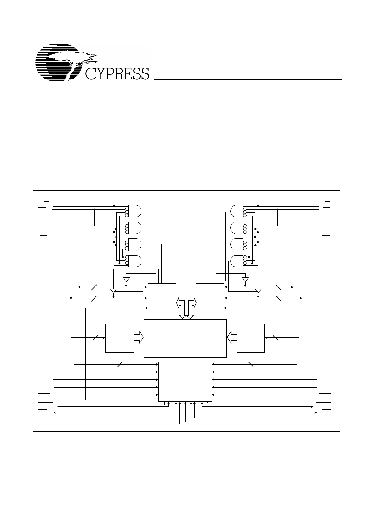
Logic Block Diagram
A0L–A
11/1213L
True Dual-Ported
RAM Array
A0R–A
11/12/13R
CE
R
OE
R
R/W
R
BUSY
R
SEM
R
INT
R
UB
R
LB
R
Address
Decode
A
0R–A11/12/13R
[2]
[2]
[3]
[3]
[5]
[5]
12/13/14
8/9
8/9
12/13/14
8/9
8/9
12/13/14 12/13/14
[4]
[4]
[4]
[4]
For the most recent information, visi t th e Cypress web site at www .cypress.com
CY7C024AV/025AV/026AV
CY7C0241AV/0251AV/036AV
2
PRELIMINARY
Functional Description
The CY7C024AV/025AV/026AV and CY7C0241AV/0251AV /
036AV are low-power CMOS 4K, 8K, and 16K x16/18 dualport static RAMs. Various arbitration schem es are incl uded o n
the devices to handle si tuations when multiple processors access the same piece of data. Two ports are provided, permitting independent, asynchronous access for reads and writes
to any location in memory. The devices can be utilized as standalone 16/18 -bit dual- port sta tic RAMs or m ult iple d e vices ca n
be combined in order to function as a 32/36-bit or wider master/slave dual-port static RAM. An M/S
pin is provided for implementing 32/ 36-bit or wi der memory applicati ons without th e
need for separate master and slave devices or additional discrete logic. Appl ication areas include in terprocessor/multiprocessor designs, communications status buffering, and dualport video/graphics memory .
Each port has independent control pins: Chip Enable (CE
),
Read or Write Enable (R/W
), and Output Enable (OE). Two
flags are provided on each port (BUSY
and INT). BUSY signals that the port is trying to access t he same location cur rently
being accessed by t he other port. The Int errupt fla g (INT
) permits communicati on between ports or systems by means of a
mail box. The semaphores are used to pass a flag, or token,
from one port to the other to indica te that a shar ed r esource i s
in use. The semaphore logic is comprised of eight shared
latches. Only one side can control the latch (semaphore) at
any time. Control of a semaphore indicates that a shared resource is in use. An automatic power-down feature is controlled independently on each port by a Chip Select (CE
) pin.
The CY7C024AV/025AV/026AV and CY7C0241AV/0251AV/
036AV are available in 100-pin Thin Quad Plastic Flatpacks
(TQFP).
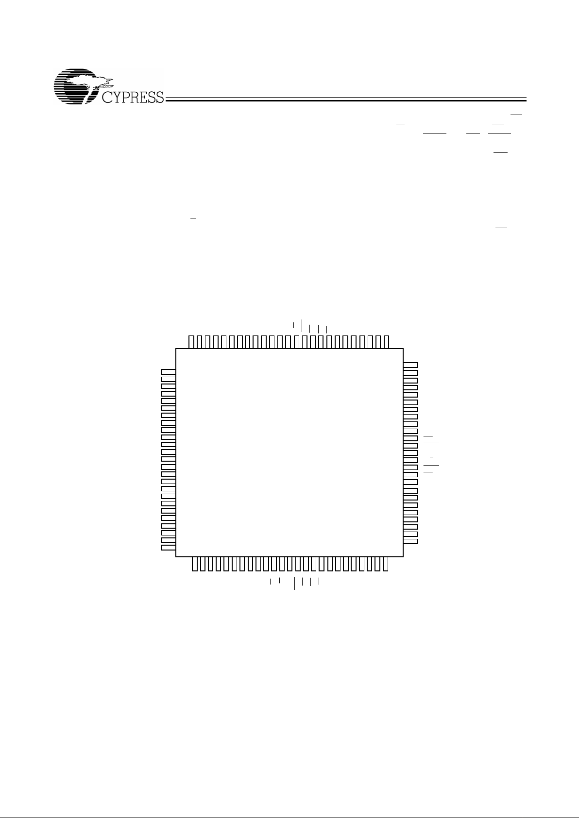
Pin Configurations
Notes:
6. A
12L
on the CY7C025AV.
7. A
12R
on the CY7C025AV.
Top Vie w
100-Pin TQFP
100 99 9798 96
2
3
1
4241
59
60
61
12
13
15
14
16
4
5
40
39
95 94
17
26
9
10
8
7
6
11
27 28 3029 31 32 3534 36 373833
67
66
64
65
63
62
68
69
70
75
73
74
72
71
89 88 8687 8593 92 84
NC
NC
NC
NC
A
5L
A
4L
INT
L
A
2L
A
0L
BUSY
L
GND
INT
R
A
0R
A
1L
NC
NC
NC
NC
I/O
10L
I/O
11L
I/O
15L
V
CC
GND
I/O
1R
I/O
2R
V
CC
9091
A
3L
M/S
BUSY
R
I/O
14L
GND
I/O
12L
I/O
13L
A
1R
A
2R
A
3R
A
4R
NC
NC
NC
NC
I/O
3R
I/O
4R
I/O
5R
I/O
6R
NC
NC
NC
NC
18
19
20
21
22
23
24
25
83 82 81 80 79 78 77 76
58
57
56
55
54
53
52
51
43 44 45 46 4748 49 50
I/O9LI/O8LI/O7LI/O6LI/O5LI/O4LI/O3LI/O
2L
GND
I/O1LI/O
0L
OE
L
SEM
L
V
CC
CE
L
UBLLBLNC
A
11LA10L
A9LA8LA7LA
6L
I/O
0R
I/O7RI/O8RI/O
9R
I/O
10R
I/O
11R
I/O
12R
I/O
13R
I/O
14R
GND
I/O
15R
Œ
R
R/W
R
GND
SEM
RCERUBRLBR
NC
A
11RA10R
A9RA8RA7RA6RA
5R
CY7C024AV (4K x 16)
R/W
L
[6]
[7]
CY7C025AV (8K x 16)
CY7C024AV/025AV/026AV
CY7C0241AV/0251AV/036AV
3
PRELIMINARY
Pin Configurations
(continued)
Notes:
8. A
12L
on the CY7C0251AV.
9. A
12R
on the CY7C0251AVC.
T op View
100- Pin TQFP
100 99 9798 96
2
3
1
4241
59
60
61
12
13
15
14
16
4
5
4039
95 94
17
26
9
10
8
7
6
11
27 28 3029 31 32 3534 36 37 3833
67
66
64
65
63
62
68
69
70
75
73
74
72
71
89 88 8687 8593 92 84
NC
NC
NC
NC
A
5L
A
4L
INT
L
A
2L
A
0L
BUSY
L
GND
INT
R
A
0R
A
1L
NC
NC
I/O
11L
I/O
12L
I/O
16L
V
CC
GND
I/O
1R
I/O
2R
V
CC
9091
A
3L
M/S
BUSY
R
I/O
15L
GND
I/O
13L
I/O
14L
A
1R
A
2R
A
3R
A
4R
NC
NC
NC
NC
I/O
3R
I/O
4R
I/O
5R
I/O
6R
NC
NC
18
19
20
21
22
23
24
25
83 82 81 80 79 78 77 76
58
57
56
55
54
53
52
51
43 44 45 46 4748 49 50
I/O9LI/O7LI/O6LI/O5LI/O4LI/O3LI/O
2L
I/O
10L
GND
I/O1LI/O
0L
OE
L
SEM
L
V
CC
CE
L
UBLLB
L
NC
A
11LA10L
A9LA8LA7LA
6L
I/O
0R
I/O
7R
I/O
16R
I/O
9R
I/O
10R
I/O
11R
I/O
12R
I/O
13R
I/O
14R
GND
I/O
15R
OE
R
R/W
R
GND
SEM
RCERUBRLBR
NC
A
11RA10R
A9RA8RA7RA6RA
5R
CY7C0241AV (4K x 18)
I/O
8L
I/O
17L
I/O
8R
I/O
17R
R/W
L
[9]
[8]
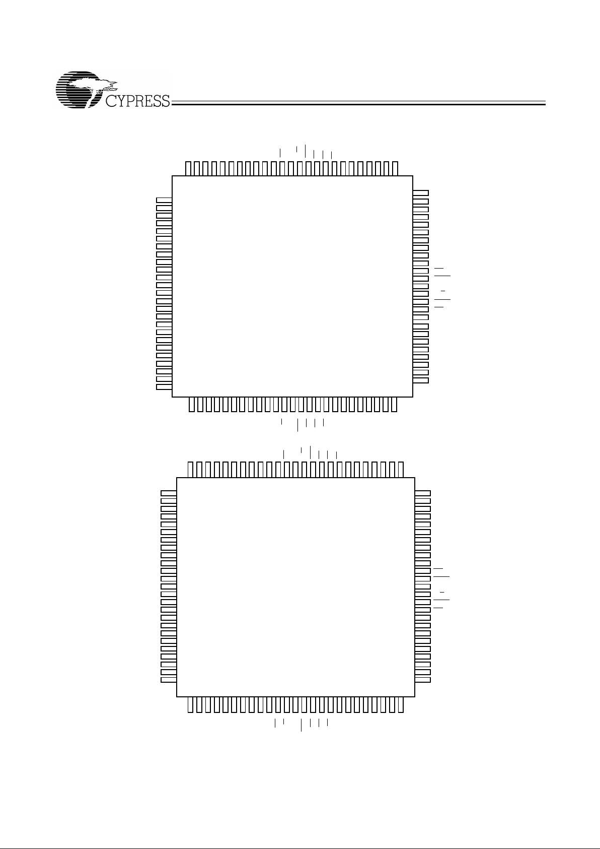
1
3
2
92 91 90 848587 868889 83 82 81 7678 77798093949596979899100
59
60
61
67
66
64
65
63
62
68
69
70
75
73
74
72
71
NC
NC
NC
A6L
A5L
A4L
INT
L
A2L
A0L
GND
M/S
A0R
A1R
A1L
A3L
BUSYR
INTR
A2R
A3R
A4R
A5R
NC
NC
NC
BUSYL
58
57
56
55
54
53
52
51
CY7C026AV (16K x 16)
NC
NC
NC
NC
I/O10L
I/O11L
I/O15L
I/O13L
I/O14L
GND
I/O0R
VCC
I/O3R
GND
I/O12L
I/O1R
I/O2R
I/O4R
I/O5R
I/O6R
NC
NC
NC
NC
VCC
17
16
15
9
10
12
11
13
14
8
7
6
4
5
18
19
20
21
22
23
24
25
I/O9L
I/O8L
I/O7L
I/O6L
I/O5L
I/O4L
I/O0L
I/O2L
I/O1L
VCC
R/WL
UBL
LBL
GND
I/O3L
SEML
CEL
A113L
A12L
A11L
A10L
A9L
A8L
A7L
OEL
34 35 36 424139 403837 43 44 45 5048 494746
A6R
A7R
A8R
A9R
A10R
A11R
CER
A13R
UBR
GND
R/WR
GND
I/O14R
LBR
A12R
OER
I/O15R
I/O13R
I/O12R
I/O11R
I/O10R
I/O9R
I/O8R
I/O7R
SEMR
3332313029282726
CY7C0251 AV (8K x 18)
CY7C024AV/025AV/026AV
CY7C0241AV/0251AV/036AV
4
PRELIMINARY
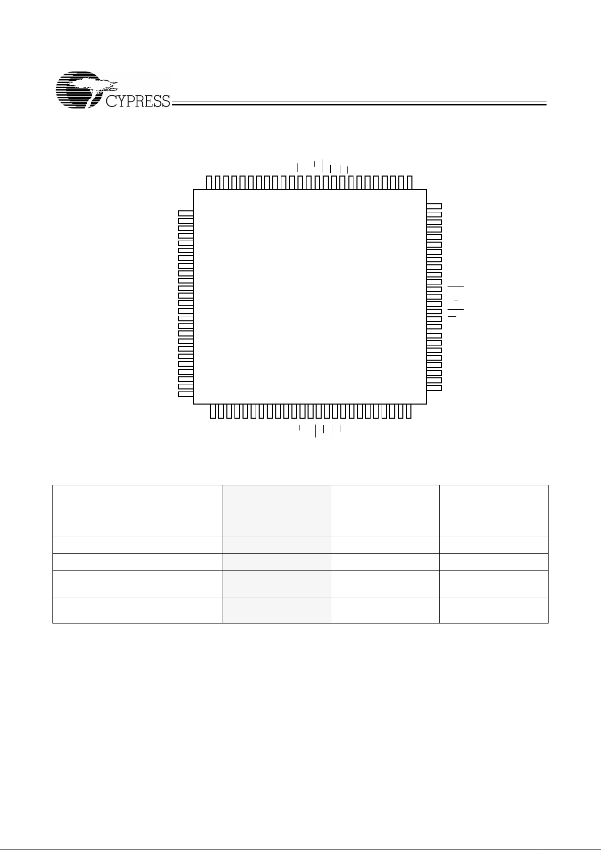
Pin Configurations
(continued)
Selection G uide
CY7C024AV/025AV/
026AV
CY7C0241AV/0251AV/
036AV
-15
[1]
CY7C024AV/025AV/
026AV
CY7C0241AV/0251AV/
036AV
-20
CY7C024AV/025AV/
026AV
CY7C0241AV/0251AV/
036AV
-25
Maximum Access Time (ns) 15 20 25
Typical Operat ing Current (mA) 125 120 115
Typical Standby Current for I
SB1
(mA)
(Both ports TTL Level)
35 35 30
Typical Standby Current for I
SB3
(µA)
(Both ports CMOS Level)
10 µA 10 µA 10 µA
Shaded areas contain advance information.
T op View
100-Pin TQFP
100 99 9798 96
2
3
1
4241
59
60
61
12
13
15
14
16
4
5
4039
95 94
17
26
9
10
8
7
6
11
27 28 3029 31 32 3534 36 37 3833
67
66
64
65
63
62
68
69
70
75
73
74
72
71
89 88 8687 8593 92 84
NC
NC
NC
A
5L
A
4L
INT
L
A
2L
A
0L
BUSY
L
GND
INT
R
A
0R
A
1L
NC
NC
I/O
11L
I/O
12L
I/O
16L
V
CC
GND
I/O
1R
I/O
2R
V
CC
9091
A
3L
M/S
BUSY
R
I/O
15L
GND
I/O
13L
I/O
14L
A
1R
A
2R
A
3R
A
4R
NC
NC
NC
I/O
3R
I/O
4R
I/O
5R
I/O
6R
NC
NC
18
19
20
21
22
23
24
25
83 82 81 80 79 78 77 76
58
57
56
55
54
53
52
51
43 44 45 46 47 48 49 50
I/O9LI/O7LI/O6LI/O5LI/O4LI/O3LI/O
2L
I/O
10L
GND
I/O1LI/O
0L
OE
L
SEM
L
V
CC
CE
L
UBLLB
L
A
11LA10L
A9LA8LA7LA
6L
I/O
0R
I/O
7R
I/O
16R
I/O
9R
I/O
10R
I/O
11R
I/O
12R
I/O
13R
I/O
14R
GND
I/O
15R
OE
R
R/W
R
GND
SEM
RCERUBRLBR
A
11RA10R
A9RA8RA7RA6RA
5R
I/O
8L
I/O
17L
I/O
8R
I/O
17R
R/W
L
CY7C036AV (16K x 18)
A
13L
A
13R
A
12L
A
12R
CY7C024AV/025AV/026AV
CY7C0241AV/0251AV/036AV
5
PRELIMINARY
Maximum Ratings
(Above which the useful lif e may be impaired. For user guidelines, not tested.)
Storage Temperature ........................ .........–65
°
C to +150°C
Ambient Temperature with
Power Applied.............................................–55
°
C to +125°C
Supply Voltage to Ground Potential...............–0.5V to +4.6V
DC V oltage Applied to
Outputs in High Z State ...........................–0.5V to V
CC
+0.5V
DC Input Voltage
[10]
.................................–0.5V to VCC+0.5V
Output Current into Outputs (LOW)............................. 20 mA
Static Discharge Voltage ........... .............. .. ............. .. >2001V
Latch-Up Current............. .. .............. ........... ............ >200 mA
Notes:
10. Pulse width < 20 ns.
11. Industrial parts are available in CY7C026AV and CY7C036AV only .
Pin Definitions
Left Port Right Por t Description
CE
L
CE
R
Chip Enable
R/W
L
R/W
R
Read/Write Enable
OE
L
OE
R
Output Enable
A0L–A
13L
A0R–A
13R
Address (A0–A11 for 4K devices; A0–A12 for 8K devices; A0–A13 for 16K)
I/O0L–I/O
17L
I/O0R–I/O
17R
Data Bus Input/Output
SEML SEM
R
Semaphore Enable
UB
L
UB
R
Upper Byte Select ( I/O8–I/O15 for x1 6 de v ices; I/O9–I/O17 for x 18 devices)
LB
L
LB
R
Lower Byte Select (I/O0–I/O7 for x16 devices; I/O0–I/O8 for x18 devices)
INT
L
INT
R
Interrupt Flag
BUSY
L
BUSY
R
Busy Flag
M/S Master or Slave Select
V
CC
Power
GND Ground
NC No Connect
Operating Range
Range
Ambient
Temperature
V
CC
Commercial 0°C to +70°C 3.3V ± 300 mV
Industrial
[11]
–40°C to +85°C 3.3V ± 300 mV
Shaded areas contain advance information.

CY7C024AV/025AV/026AV
CY7C0241AV/0251AV/036AV
6
PRELIMINARY
Notes:
12. f
MAX
= 1/tRC = All inputs c ycling at f = 1/tRC (except output enab le) . f = 0 mea ns no add ress or control lines change . T his appl ies onl y to inpu ts at CM OS level standby I
SB3
.
13. Tested initially and after any design or process changes that may affect these parameters.
Electrical Characteristics
Over the Operating Range
Parameter Description
CY7C024AV/025AV/026AV
CY7C0241AV/0251AV/036AV
Unit
-15
[1]
-20 -25
Min. Typ. Max. Min. Typ. Max. Mi n. Typ. Max.
V
OH
Output HIGH Voltage (VCC=3.3V) 2.4 2.4 2.4 V
V
OL
Output LO W Voltage 0.4 0.4 0.4 V
V
IH
Input HIGH Voltage 2.0 2.0 2.0 V
V
IL
Input LOW Voltage 0.8 0.8 0.8 V
I
OZ
Output Leakage Curr ent –10 10 –10 10 –10 10 µA
I
IX
Input Leakage Current –10 10 –10 10 –10 10 µA
I
CC
Operating Cur rent (V
CC
= Max.,
I
OUT
= 0 mA) Outputs Disabled
Com’l.
125 185 120 175 115 165 mA
Ind.
[11]
135 185 mA
I
SB1
Standby Current (Both Por ts TTL
Level) CE
L
& CER ≥ VIH, f = f
MAX
Com’l. 35 50 35 45 30 40 mA
Ind.
[11]
40 50 mA
I
SB2
Standby Current (One Port TTL
Level) CE
L
| CER ≥ VIH, f = f
MAX
Com’l. 80 120 75 110 65 95 mA
Ind.
[11]
75 105 mA
I
SB3
Standby Curre nt (Both Ports CMOS
Level) CE
L
& CER ≥ V
CC
−0.2V , f = 0
Com’l.
10 500 10 500 10 500 µA
Ind.
[11]
10 500
µA
I
SB4
Standby Current (One Port CMOS
Level) CE
L
| CER ≥ VIH, f = f
MAX
[12]
Com’l. 75 105 70 95 60 80 mA
Ind.
[11]
70 90 mA
Shaded areas contain advance information.
Capacitance
[13]
Parameter Description Test Conditions Max. Unit
C
IN
Input Capacitance TA = 25°C, f = 1 MHz,
V
CC
= 3.3V
10 pF
C
OUT
Output Capacitance 10 pF
AC Test Loads and Waveforms
3.0V
GND
90%
90%
10%
3ns
3
ns
10%
ALL INPUTPULSES
(a) Normal Load (Load
1)
R1= 590
Ω
3.3V
OUTPUT
R2= 435
Ω
C= 30
pF
V
TH
=1.4V
OUTPUT
C=
30pF
(b) Thévenin Equivalent (Load 1)
(c)Three-State Delay(Load2)
R1= 590
Ω
R2= 435
Ω
3.3V
OUTPUT
C= 5pF
R
TH
=250
Ω
≤
≤
including scope and jig)
(Used for t
LZ
, tHZ, t
HZWE
, & t
LZWE
 Loading...