

Cypress Semiconductor CY7C0251-35AC, CY7C0251-25AI, CY7C0251-25AC, CY7C0251-15AI, CY7C0251-15AC Datasheet
...
4K x 16/18 and 8K x 16/18 Dual-Port
Static RAM with Sem, Int, Bus
y
CY7C024/0241
CY7C025/0251
Cypress Semiconductor Corporation
• 3901 North First Street • San Jose • CA 95134 • 408-943-2600
Januar
y 8,
1999
5
1
Features
• True Dual-P orted memory cells which allow
simultaneous reads of the same memory location
• 4K x 16 organizatio n (CY7C024)
• 4K x 18 organizatio n (CY7C0241)
• 8K x 16 organizatio n (CY7C025)
• 8K x 18 organizatio n (CY7C0251)
• 0.65-micron CMOS for optimum speed/power
• High-speed access: 15 ns
• Low operating power: I
CC
= 150 mA (typ.)
• Fully asynchronous operation
• Automatic power-down
• Expandable data bus to 32/36 bits or more using
Master/Slave chip select when using more than one
device
• On-chip arbitration logic
• Semaphores inc luded to permit software handshaki ng
between ports
•INT
flag for port-to-po rt commu n ic a ti o n
• Separate upper-byte and lower-byte control
• Pin select for Master or Slave
• Av ailable in 84-pin PLCC and 100-pin TQFP
• Pin-compatibl e and functionally equivalent to
IDT7024/IDT7025
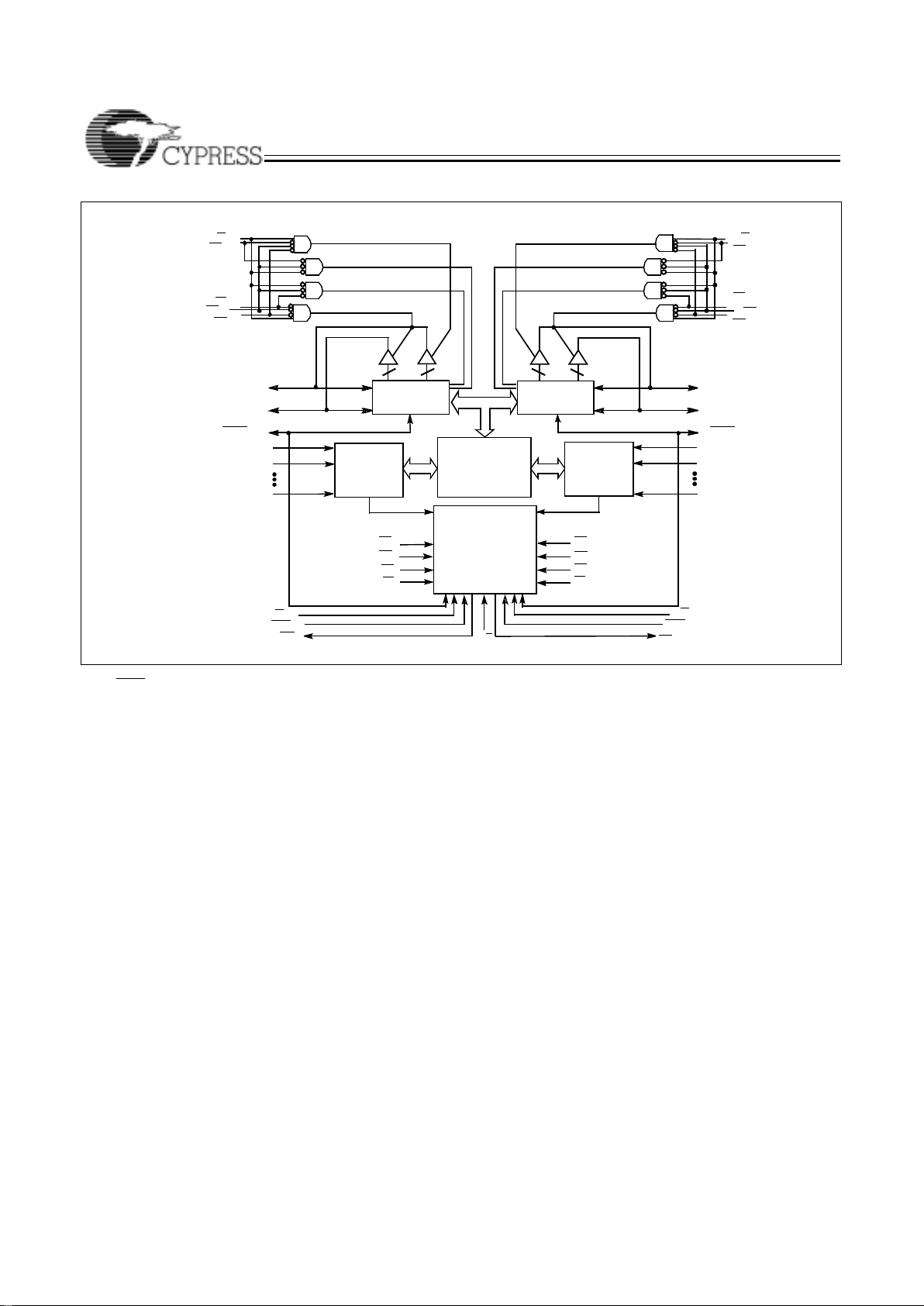
Functional Description
The CY7C024/0241 and CY7C025/0251 are low-power
CMOS 4K x 16/18 and 8K x 16/18 dual-port static RAM s. Various arbitration schemes are included on the CY7C024/0241
and CY7C025/0251 to handle situations when multiple processors access the same piece of data. Two ports are provided, permitting independent, asynchronous access for reads
and writes to any location in memory . The CY7C024/0241 and
CY7C025/0251 can be utilized as standalone 16-/18-bit dual-port static RAMs or multiple devices can be combined in
order to function as a 32-/36-bit or wider master/slave dual-port static RAM. An M/S
pin is provided for implementing
32-/36-bit or wider memory applications without the need for
separate mast er and s la v e d e vice s o r addi tion al di scret e logic .
Application areas include interprocessor/multiprocessor designs, communications status buffering, and dual-port video/graphic s me mo ry.
Each port has independent control pins: Chip Enable (CE
),
Read or Write Enable (R/W
), and Output Enable (OE). T w o flags
are provided on each port (BUSY
and INT). BUSY signals that the
port is tr yi ng to access the same location cur rently being acce ssed
by the other port. The Inte rrupt Flag (INT
) permits co mmunication
between ports or systems by means of a mail box. The semaphores
are used to pass a flag, or token, from one port to the other to indicate
that a shared resource is in use. The semaphore logic is comprised
of eight shared latches. Only o ne side can control the latch (semaphore) at any time. Control of a semaphore indicates that a shar ed
resource is in use. An a utomatic power-down feature is controlled
independently on each port by a chip select (CE
) pin.
The CY7C024/0241 and CY7C025/0251 are available in
84-pin PLCCs (CY7C024 and CY7C025 only) and 100-pin
Thin Quad Plastic Flatpack (TQFP).
Static RAM wit h Sem , Int, Bu sy
CY7C024/0241
CY7C025/0251
2
v
Notes:
1. BUSY
is an output in master mode and an input in slave mode.
2. I/O0 –I/O8 on the CY7C0241/0251.
3. I/O9 –I/O17 on the CY7C0241/0251.
7C024–1
R/W
L
UB
L
LB
L
CE
L
OE
L
A
0L
R/W
R
UB
R
CE
R
OE
R
CE
L
OE
L
UB
L
UB
R
I/O8L–I/O
15L
INTERRUPT
SEMAPHORE
ARBITRATION
CONTROL
I/O
MEMORY
ARRAY
ADDRESS
DECODER
SEM
L
SEM
R
BUSY
L
INT
L
INT
R
M/S
CONTROL
I/O
LB
L
LB
R
I/O0L–I/O
7L
R/W
L
R/W
R
LB
R
CE
R
OE
R
A
0R
I/O8RI/O
15R
BUSY
R
I/O
0R
I/O
7R
(CY7C025/0251) A
12L
A
12R
(CY7C025/0251)
[1] [1]
Logic Block Diagram
–
–
ADDRESS
DECODER
A
11L
A
11R
[2]
[3]
[2]
[3]
CY7C024/0241
CY7C025/0251
3
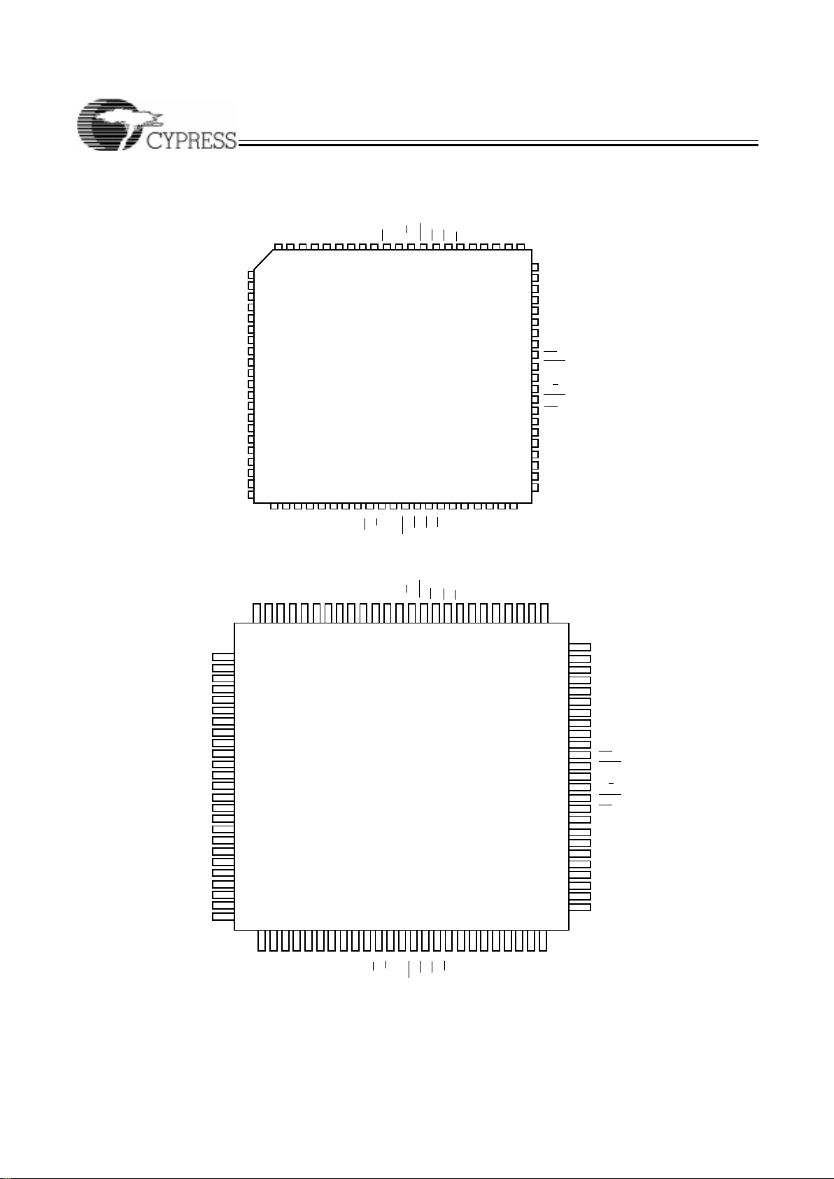
Pin Configurations
Notes:
4. A
12L
on the CY7C025/0251.
5. A
12R
on the CY7C025/0251.
L
L
L
7C024–1
Top View
84-Pin PLCC
A
7L
OE
CE
NC
I/O
I/O
I/O
I/O
I/O
I/O
A
6L
A
5L
A
4L
A
3L
A
2L
INT
L
BUSY
L
M/S
BUSY
R
A
1R
A
2R
I/O
8L
I/O
9L
I/O
10L
I/O
11L
I/O
12L
I/O
13L
I/O
15L
V
CC
I/O
0R
I/O
2R
I/O
1R
I/O
3R
I/O
4R
I/O
5R
AAA
A
A
3R
A
4R
A
5R
A
6R
I/O
6R
I/O
7R
I/O
8R
GND
I/O
14L
A
1L
I/O
R/W
SEM
UB
A
0L
GND
INT
R
A
0R
GND
GND
7L6L5L4L3L
2L
0L
L
L
11L
10L
9L
8L
I/O
1L
V
CC
LB
L
OE
CE
I/O
I/O
I/O
I/O
I/O
A
A
A
A
GND
I/O
R/W
SEM
UB
9R
10R
11R
12R
13R
15R
R
R
R
R
10R
9R
8R
7R
I/O
14R
R
LB
R
A
11R
NC
GND
V
CC
63
62
61
60
59
58
57
56
55
54
535251504948
47
46454443
1234567891011
12
13
14
15
16
17
18
19
20
21
64
65
66
67
68
69
70
71
72
73
74
75767778798081828384
42414039383736353433
32
31
30
29
28
27
26
25
24
23
22
CY7C024/5
[4]
[5]
Top View
100-Pin TQFP
100 99 9798 96
2
3
1
4241
59
60
61
12
13
15
14
16
4
5
4039
95 94
17
26
9
10
8
7
6
11
27 28 3029 31 32 3534 36 37 3833
67
66
64
65
63
62
68
69
70
75
73
74
72
71
89 88 8687 8593 92 84
NC
NC
NC
NC
A
5L
A
4L
INT
L
A
2L
A
0L
BUSY
L
GND
INT
R
A
0R
A
1L
NC
NC
NC
NC
I/O
10L
I/O
11L
I/O
15L
V
CC
GND
I/O
1R
I/O
2R
V
CC
9091
A
3L
M/S
BUSY
R
I/O
14L
GND
I/O
12L
I/O
13L
A
1R
A
2R
A
3R
A
4R
NC
NC
NC
NC
I/O
3R
I/O
4R
I/O
5R
I/O
6R
NC
NC
NC
NC
18
19
20
21
22
23
24
25
83 82 81 80 79 78 77 76
58
57
56
55
54
53
52
51
43 44 45 46 47 48 49 50
I/O9LI/O8LI/O7LI/O6LI/O5LI/O4LI/O3LI/O
2L
GND
I/O1LI/O
0L
OE
L
SEM
L
V
CC
CE
L
UBLLB
L
NC
A
11LA10L
A9LA8LA7LA
6L
7C024–2
I/O
0R
I/O7RI/O8RI/O
9R
I/O
10R
I/O
11R
I/O
12R
I/O
13R
I/O
14R
GND
I/O
15R
Œ
R
R/W
R
GND
SEM
RCERUBRLBR
NC
A
11RA10R
A9RA8RA7RA6RA
5R
CY7C024/5
R/W
L
[4]
[5]
CY7C024/0241
CY7C025/0251
4
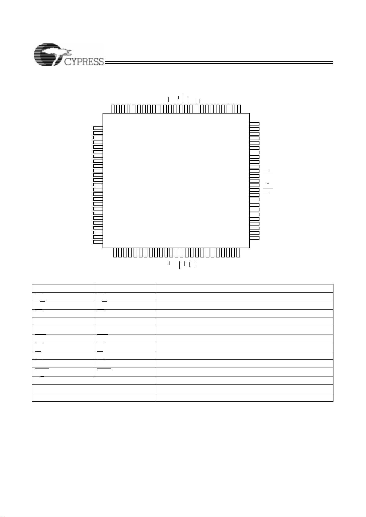
Pin Definitions
Left Port Right Port Description
CE
L
CE
R
Chi p E nable
R/W
L
R/W
R
Read/Write Enable
OE
L
OE
R
Output Enable
A0L–A
11/12L
A0R–A
11/12R
Address
I/O0L–I/O
15/17L
I/O0R–I/O
15/17R
Data Bus Input/Output
SEML SEM
R
Semaphore Enable
UB
L
UB
R
Upper Byte Select
LB
L
LB
R
Lower Byte Select
INT
L
INT
R
Interrup t F lag
BUSY
L
BUSY
R
Busy Flag
M/S Master or Slave Select
V
CC
Power
GND Ground
Pin Configurations
(continued)
Top Vi ew
100-Pin TQFP
100 99 9798 96
2
3
1
4241
59
60
61
12
13
15
14
16
4
5
4039
95 94
17
26
9
10
8
7
6
11
27 28 3029 31 32 3534 36 37 3833
67
66
64
65
63
62
68
69
70
75
73
74
72
71
89 88 8687 8593 92 84
NC
NC
NC
NC
A
5L
A
4L
INT
L
A
2L
A
0L
BUSY
L
GND
INT
R
A
0R
A
1L
NC
NC
I/O
11L
I/O
12L
I/O
16L
V
CC
GND
I/O
1R
I/O
2R
V
CC
9091
A
3L
M/S
BUSY
R
I/O
15L
GND
I/O
13L
I/O
14L
A
1R
A
2R
A
3R
A
4R
NC
NC
NC
NC
I/O
3R
I/O
4R
I/O
5R
I/O
6R
NC
NC
18
19
20
21
22
23
24
25
83 82 81 80 79 78 77 76
58
57
56
55
54
53
52
51
43 44 45 46 47 48 49 50
I/O9LI/O7LI/O6LI/O5LI/O4LI/O3LI/O
2L
I/O
10L
GND
I/O1LI/O
0L
OE
L
SEM
L
V
CC
CE
L
UBLLB
L
NC
A
11LA10L
A9LA8LA7LA
6L
7C024–3
I/O
0R
I/O
7R
I/O
16R
I/O
9R
I/O
10R
I/O
11R
I/O
12R
I/O
13R
I/O
14R
GND
I/O
15R
OE
R
R/W
R
GND
SEM
RCERUBRLBR
NC
A
11RA10R
A9RA8RA7RA6RA
5R
CY7C0241/0251
I/O
8L
I/O
17L
I/O
8R
I/O
17R
R/W
L
[5]
[4]
CY7C024/0241
CY7C025/0251
5
Maximum Ratings
(Above which the useful lif e m ay be impaired. For user guidelines, not tested.)
Storage Temperature ...... .......... .. ... .......... ..–65
°
C to +150°C
Ambient Temperature with
Power Applied .............................................–55
°
C to +125°C
Supply Voltage to Ground Potential ............... –0.3V to +7.0V
DC V oltage Applied to Outputs
in High Z State...............................................–0.5V to +7.0V
DC Input Voltage
[6]
......................................... –0.5V to +7.0V
Output Current into Outputs (LOW)............................. 20 mA
Static Discharge Voltage ........................... ............... >2001V
(per MIL-STD-883, Method 3015)
Latch-Up Current.................................. ............ ...... >200 mA
Selection Guide
7C024/0241–15
7C025/0251–15
7C024/0241–25
7C025/0251–25
7C024/0241–35
7C025/0251–35
7C024/0241–55
7C025/0251–55
Maximum Access Time (ns) 15 25 35 55
Typical Operating Current (mA) 190 170 160 150
Typical Standby Current for I
SB1
(mA) 50 40 30 20
Operating Range
Range
Ambient
T em perature V
CC
Commercial 0°C to +70°C 5V ± 10%
Industrial –40°C to +85°C 5V ± 10%
Electrical Characteristics
Over the Op erating Range
Parameter Description Test Conditions
7C024/0241–15
7C025/0251–15
7C024/0241–25
7C025/0251–25
UnitMin. Typ. Max. Min. Typ. Max.
V
OH
Output HIGH Voltage VCC = Min., IOH = –4.0 mA 2.4 2.4 V
V
OL
Output LOW Voltage VCC = Min., IOL = 4.0 mA 0.4 0.4 V
V
IH
Input HIGH Voltage 2.2 2.2 V
V
IL
Input LOW Voltage –0.7 0.8 –0. 7 0.8 V
I
IX
Input Leakage Current GND ≤ VI ≤ V
CC
–10 +10 –10 +10 µA
I
OZ
Output Leakage
Current
Output Disabled,
GND ≤ V
O
≤ V
CC
–10 +10 –10 +10 µA
I
CC
Operating Current VCC = Max., I
OUT
= 0 mA,
Outputs Disabled
Com’l 190 300 170 250 mA
Ind 200 320 170 290
I
SB1
Standby Current
(Both Ports TTL Levels)
CEL and CER ≥ VIH,
f = f
MAX
[7]
Com’l 5070 4060mA
Ind 50 70 75
I
SB2
Standby Current
(On e Port TTL Level)
CEL or CER ≥ VIH,
f = f
MAX
[7]
Com’l 120 180 100 150 mA
Ind 120 180 100 170
I
SB3
Standby Current
(Both Ports CMOS
Lev els)
Both Ports CE
and CER ≥
V
CC
– 0.2V, VIN ≥ VCC – 0.2V
or V
IN
≤ 0. 2V, f = 0
[7]
Com’l 3 15 3 15 mA
Ind 3 15 3 15
I
SB4
Standby Current
(Both Ports CMOS
Lev els)
One Port C EL or
CE
R
≥ VCC – 0.2V,
V
IN
≥ V
CC
– 0.2V or VIN ≤ 0.2V,
Active Port Outputs, f = f
MAX
[7]
Com’l 110 160 90 130 mA
Ind 110 160 90 150
Notes:
6. Pulse width < 20 ns.
7. f
MAX
= 1/tRC = All inputs cycl ing at f = 1/tRC (except outpu t enab le) . f = 0 means no ad dress or contr ol li nes change . T his applies only to i np uts at C MOS level standby I
SB3
.
CY7C024/0241
CY7C025/0251
6
Electrical Characteristics
Over the Op erating Range (continued)
7C024/0241–35
7C025/0251–35
7C024/0241–55
7C025/0251–55
Parameter Description Test Conditions Min. Typ. Max. Min. Typ. Max. Unit
V
OH
Output HIGH Voltage VCC = Min., IOH = –4.0 mA 2.4 2.4 V
V
OL
Output LOW Voltage VCC = Min., IOL = 4.0 mA 0.4 0.4 V
V
IH
Input HIGH Voltage 2.2 2.2 V
V
IL
Input LOW Voltage –0.7 0.8 –0.7 0.8 V
I
IX
Input Leakage Current GND ≤ VI ≤ V
CC
–10 +10 –10 +10 µA
I
OZ
Output Leakage Current Output Disabled, GND ≤ VO ≤ V
CC
–10 +10 –10 +10 µA
I
CC
Operating Curr ent VCC = Max., I
OUT
= 0 mA,
Outputs Disabled
Com’l 160 230 150 230 mA
Ind 160 260 150 260
I
SB1
Standby Current
(Both Ports TTL Levels)
CEL and CER ≥ VIH,
f = f
MAX
[7]
Com’l 30 50 20 50 mA
Ind 30 65 20 65
I
SB2
Standby Current
(One P ort TTL Level)
CEL or CER ≥ VIH,
f = f
MAX
[7]
Com’l 8 5 135 75 135 mA
Ind 85 150 75 150
I
SB3
Standby Current
(Both Ports CMOS
Levels)
Both Ports CE
and CER ≥
V
CC
– 0.2V , VIN ≥ VCC – 0.2V
or V
IN
≤ 0.2V, f = 0
[7]
Com’l 3 15 3 15 mA
Ind 3 15 3 15
I
SB4
Standby Current
(Both Ports CMOS
Levels)
One Port CEL or
CE
R
≥ VCC – 0.2V ,
V
IN
≥ VCC – 0.2V or VIN ≤ 0.2V,
Active P ort Outputs , f = f
MAX
[7]
Com’l 8 0 120 70 120 mA
Ind 80 135 70 135
Capacitance
[8]
Parameter Description Test Conditions Max. Unit
C
IN
Input Capacitance TA = 25°C, f = 1 MHz,
V
CC
= 5.0V
10 pF
C
OUT
Output Capacitance 10 pF
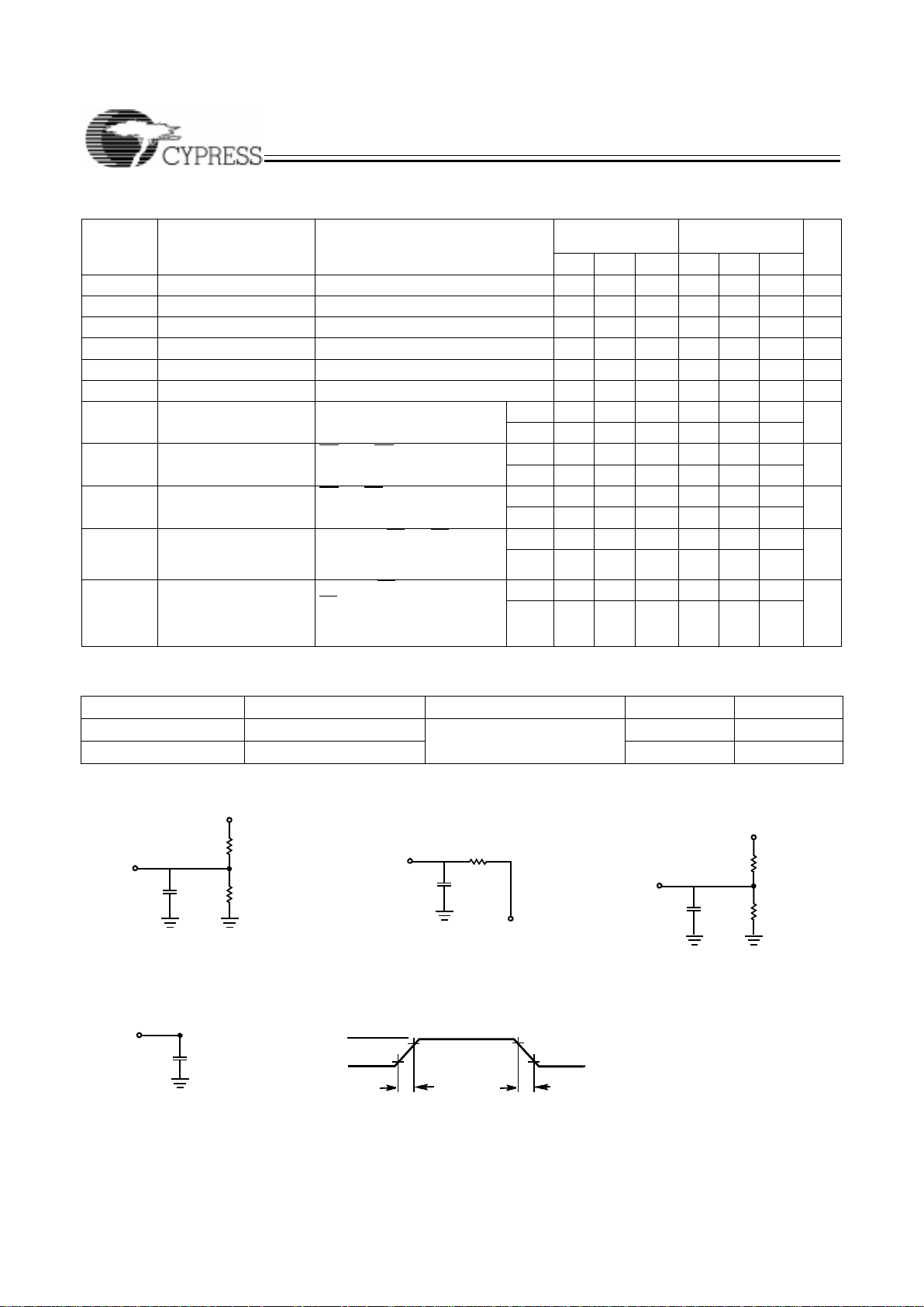
AC Test Loads and Waveforms
Note:
8. Tested initially and after any design or process changes that may affect these parameters.
3.0V
GND
90%
90%
10%
3ns
3
ns
10%
ALL INPUTPULSES
(a) Normal Load(Load
1)
R1= 893
Ω
5
V
OUTPUT
R2= 347
Ω
C= 30
pF
V
TH
=1.4V
OUTPUT
C=
30pF
(b) Thévenin Equivalent (Load 1)
(c)Three-State Delay(Load
3)
C = 30 pF
OUTPUT
Load (Load 2)
7C024–8 7C024–9 7C024–10
7C024–11 7C024–12
R1= 893
Ω
R2= 347
Ω
5V
OUTPUT
C= 5pF
R
TH
=250
Ω
≤
≤

CY7C024/0241
CY7C025/0251
7
Switching C h aracteristics
Over the Operating Range
[9]
7C024/0241–15
7C025/0251–15
7C024/0241–25
7C025/0251–25
7C024/0241–35
7C025/0251–35
7C024/0241–55
7C025/0251–55
Parameter Description Min. Max. Min. Max. Min. Max. Min. Max. Unit
READ CYCLE
t
RC
Read Cycle Time 15 25 35 55 ns
t
AA
Address to Data Valid 15 25 35 55 ns
t
OHA
Output Hold F rom
Address Change
3 3 3 3 ns
t
ACE
[10]
CE LOW to Data Valid 15 25 35 55 ns
t
DOE
OE LOW to Data Valid 10 13 20 25 ns
t
LZOE
[11, 12, 13]
OE Low to Lo w Z 3 3 3 3 ns
t
HZOE
[11,12, 13]
OE HIGH to High Z 10 15 20 25 ns
t
LZCE
[11, 12, 13]
CE LOW to Low Z 3 3 3 3 ns
t
HZCE
[11, 1 2, 13]
CE HIGH to High Z 10 15 20 25 ns
t
PU
[13]
CE LOW to Power-Up 0 0 0 0 ns
t
PD
[13]
CE HIGH to Power-Down 15 25 25 55 ns
t
ABE
[10]
Byte Enable Access Time 15 25 35 55 ns
WRITE CYCLE
t
WC
Write Cycle Time 15 25 35 55 ns
t
SCE
[10]
CE LOW to Write End 12 20 30 35 ns
t
AW
Address Set-Up to Write End 12 20 30 35 ns
t
HA
Address Hold From
Write End
0 0 0 0 ns
t
SA
[10]
Address Set-Up to
Write Start
0 0 0 0 ns
t
PWE
Write Pulse Width 12 20 25 35 ns
t
SD
Data Set-Up to Write End 10 15 15 20 ns
t
HD
Data Hold From Write End 0 0 0 0 ns
t
HZWE
[12, 13]
R/W LO W to High Z 10 15 20 25 ns
t
LZWE
[12, 13]
R/W HIGH to Low Z 0 0 0 0 ns
t
WDD
[14]
Write Pulse to Data Delay 30 50 60 70 ns
t
DDD
[14]
Write Data V alid to Read
Data Valid
25 35 35 45 ns
Notes:
9. Test conditions assume signal transition time of 3 ns or less, timing reference levels of 1.5V, input pulse levels of 0 to 3.0V, and output loading of the specified
I
OI/IOH
and 30-pF load capac itance.
10. To access RAM, CE
=L, UB=L, SEM=H. To access semaphore, CE=H and SEM =L. Ei ther c ondition m ust be valid fo r the ent ire t
SCE
time.
11. At any given temperature and voltage condition for any given device, t
HZCE
is less than t
LZCE
and t
HZOE
is less than t
LZOE
.
12. Test conditions used are Load 3.
13. This parameter is guaranteed but not tested.
14. For information on port-to-port delay through RAM cells from writing port to reading port, refer to Read Timing with Busy waveform.

CY7C024/0241
CY7C025/0251
8
Data Retention Mode
The CY7C024/0241 is designed with battery backup in mind.
Data retention v oltage and sup ply current are guarant eed over
temperature. The following rules insure data ret ention:
1. Chip enabl e (CE
) must be held HIGH during data retention, with-
in V
CC
to VCC – 0.2V.
2. CE
must be kept between VCC – 0.2V and 70% of VCC
during the power-up and power-down transitions.
3. The RAM can begin operati on >t
RC
after VCC reac h e s the
minimum operating voltage (4.5 volts).
BUSY TIMING
[15]
t
BLA
BUSY LOW from Address
Match
15 20 20 45 ns
t
BHA
BUSY HIGH from Address
Mismatch
15 20 20 40 ns
t
BLC
BUSY LOW from CE LOW 15 20 20 40 ns
t
BHC
BUSY HIGH from CE HIGH 15 20 20 35 ns
t
PS
Port Set-Up for Priority 5 5 5 5 ns
t
WB
R/W HIGH after BUSY
(Slave )
0 0 0 0 ns
t
WH
R/W HIGH after BUSY
HIGH (Slave)
13 20 30 40 ns
t
BDD
[16]
BUSY HIGH to Data Valid Note
16
Note
16
Note
16
Note 16ns
INTERRUPT TIMING
[15]
t
INS
INT Set Time 15 20 25 30 ns
t
INR
INT Reset Time 15 20 25 30 ns
SEMAPHORE TIMING
t
SOP
SEM Flag Update Pulse (OE
or SEM
)
10 12 15 20 ns
t
SWRD
SEM Flag Write to Read
Time
5 10 10 15 ns
t
SPS
SEM Flag Contention
Window
5 10 10 15 ns
t
SAA
SEM Address Access Time 15 25 35 55 ns
Notes:
15. Test conditions used are Load 2.
16. t
BDD
is a calculated pa rameter and is t he g reater of t
WDD–tPWE
(actual) or t
DDD–tSD
(actu al ).
Switching C h aracteristics
Over the Operating Range
[9]
(continued)
7C024/0241–15
7C025/0251–15
7C024/0241–25
7C025/0251–25
7C024/0241–35
7C025/0251–35
7C024/0241–55
7C025/0251–55
Parameter Description Min. Max. Min. Max. Min. Ma x. Min. Max. Unit
Timing
Parameter Test Conditions
[17]
Max. Unit
ICC
DR1
@ VCCDR = 2V 1.5 mA
Note:
17. CE
= VCC, Vin = GND to VCC, TA = 25°C. This parameter is guar a nteed b ut not
tested.
Data Retention Mode
7C024–13
4.5V
4.5V
V
CC
>
2.0V
V
CC
to VCC– 0.2V
V
CC
CE
t
RC
V
IH

CY7C024/0241
CY7C025/0251
9
Switching Waveforms
Notes:
18. R/W
is HIGH for read cycles
19. Device is continuously selected CE = VIL and UB or LB = VIL. This waveform cannot be used for semaphore reads.
20. OE
= VIL.
21. Address valid prior to or coincident with CE
transition LOW.
22. To access RAM, CE
= VIL, UB or LB = VIL, SEM = VIH. To access semaphore, CE = VIH, SEM = VIL.
t
RC
t
AA
t
OHA
DATA VALIDPREVIOUS DATA V ALID
DATA OUT
ADDRESS
7C024–14
t
OHA
Read Cycle No. 1 (Either P ort Address Acc ess)
[18, 19, 20]
t
ACE
t
LZOE
t
DOE
t
HZOE
t
HZCE
DATA VALID
t
LZCE
t
PU
t
PD
7C024–15
I
SB
I
CC
DATA OUT
OE
CE and
LB
or UB
CURRENT
Read Cycle No. 2 (Either Port CE/OE Access)
[18, 21, 22]
UB or LB
DATA OU T
7C024–16
t
RC
ADDRESS
t
AA
t
OHA
CE
t
LZCE
t
ABE
t
HZCE
t
HZCE
t
ACE
t
LZCE
Read Cycle No. 3 (Eithe r Port)
[18,20,21, 21, 22]

CY7C024/0241
CY7C025/0251
10
Notes:
23. R/W
must be HIGH during all addr ess transi tions.
24. A write occurs during the overlap (t
SCE
or t
PWE
) of a LO W CE or SEM and a LO W UB or LB .
25. t
HA
is measured from the ea rlier of CE or R/W or (SEM or R /W) going HI GH at th e end of writ e cycle .
26. If OE
is LOW during a R/W controlled write cy cle, the write pulse widt h must be the larger of t
PWE
or (t
HZWE
+ tSD) to al low th e I/O driv er s to t urn off and data to be plac ed on
the bus f or the re quired t
SD
. If OE is HIGH d uring an R/W contr oll ed write cy cle, th is r equirement does not apply and t he writ e pulse c an be as short as the s pecifi ed t
PWE
.
27. To access RAM, CE
= VIL, SEM = VIH.
28. To access upper byte, CE
= VIL, UB = VIL, SEM = VIH.
To access lower byte, CE
= VIL, LB = VIL, SEM = VIH.
29. Transition is measured ±500 mV from steady state w ith a 5 -pF l oad (i ncluding s cope an d ji g). This par a meter i s sampl ed and not 100% t ested.
30. During this period, the I/O pins are in the output state, and input signals must not be applied.
31. If the CE
or SEM LOW transi tion occ urs simul taneously with or after th e R/W L OW tr a nsition , the output s remain in the high-impe dance s tate .
Switching Waveforms
(continued)
7C024–17
t
AW
t
WC
t
PWE
t
HD
t
SD
t
HA
CE
R/W
OE
DAT A OUT
DATA IN
ADDRESS
t
HZOE
t
SA
t
HZWE
t
LZWE
Write Cycle No. 1: R/W Controlled Timing
[23,24,25,26]
[29]
[29]
[26]
[27,28]
NOTE 30
NOTE 30
7C024–18
t
AW
t
WC
t
SCE
t
HD
t
SD
t
HA
CE
R/W
DATA IN
ADDRESS
t
SA
Write Cycle No. 2: CE Contr oll ed Timing
[23,24,25,31]
[27,28]

CY7C024/0241
CY7C025/0251
11
Notes:
32. CE
= HIGH for the duration of the above timing (both write and read cycle).
33. I/O0R = I/O0L = LOW (request semaphore); CER = CEL = HIGH.
34. Semaphores are reset (available to both ports) at cycle start.
35. If t
SPS
is violated, the s emaphore w ill de finitel y be obt ained b y one side or the ot her, but whic h side w ill g et the semaphor e is unpredictable.
Switching Waveforms
(continued)
t
SOP
t
AA
7C024–19
VALID ADRESS VALID ADRESS
t
HD
DAT AINVALID
DAT A
OUT
VALID
t
OHA
t
AW
t
HA
t
ACE
t
SOP
t
SCE
t
SD
t
SA
t
PWE
t
SWRD
t
DOE
WRITE CYCLE READ CYCLE
OE
R/W
I/O
0
SEM
A0–A
2
Semaphore Read After Write Timing, Either Side
[32]
MA TCH
7C024–20
t
SPS
A0L–A
2L
MATCH
R/W
L
SEM
L
A0R–A
2R
R/W
R
SEM
R
Timing Diagram of Semaphore Contention
[33,34,35 ]

CY7C024/0241
CY7C025/0251
12
Note:
36. CE
L
= CER = LOW.
Switching Waveforms
(continued)
VALID
t
DDD
t
WDD
MATCH
MATCH
R/W
R
DATA IN
R
DAT A
OUTL
7C024–21
t
WC
ADDRESS
R
t
PWE
VALID
t
SD
t
HD
ADDRESS
L
t
PS
t
BLA
t
BHA
t
BDD
BUSY
L
Timing Diagram of Read with BUSY (M/S=HIGH)
[36]
t
PWE
R/W
BUSY
t
WB
t
WH
7C024–22
Write Timing with Busy Input (M/S=LOW)

CY7C024/0241
CY7C025/0251
13
Note:
37. If t
PS
is violated, the b us y s ignal will be asserted on one side or the other , b ut ther e is no gu ar antee to wh ich side BUSY will be asserted.
Switching Waveforms
(continued)
ADDRESS MATCH
t
PS
t
BLC
t
BHC
ADDRESS MATCH
t
PS
t
BLC
t
BHC
CERValidFirst:
7C024–23
ADDRESS
L,R
BUSY
R
CE
L
CE
R
BUSY
L
CE
R
CE
L
ADDRESS
L,R
7C024–24
Busy Timing Diagram No.1 (CE Arbitration)
[37]
CELV ali d First:
ADDRESS MATCH
t
PS
ADDRESS
L
BUSY
R
ADDRESS MISMATCH
t
RC
or t
WC
t
BLA
t
BHA
ADDRESS
R
ADDRESS MATCH ADDRESS MISMATCH
t
PS
ADDRESS
L
BUSY
L
tRCor t
WC
t
BLA
t
BHA
ADDRESS
R
Right AddressValid First:
7C024–25
7C024–26
Busy Timing Diagram No.2 (Address Arbitration)
[37]
Left Address Valid First

CY7C024/0241
CY7C025/0251
14
Notes:
38. t
HA
depends on which enab l e pin (CEL or R/WL) is deasserted first.
39. t
INS
or t
INR
depends on which enabl e pin (CEL or R/WL) is asserted last.
Switching Waveforms
(continued)
Interrupt Timing Diagrams
WRITE FFF (1FFF CY7C025)
t
WC
Right SideClears INTR:
t
HA
READ FFF
t
RC
t
INR
WRITE FFE (1FFE CY7C025)
t
WC
Right SideSets INT
L
:
Left Side Sets INT
R
:
Left SideClears INT
L
:
READ FFE
t
INR
t
RC
ADDRESS
R
CE
L
R/W
L
INT
L
OE
L
ADDRESS
R
R/W
R
CE
R
INT
L
ADDRESS
R
CE
R
R/W
R
INT
R
OE
R
ADDRESS
L
R/W
L
CE
L
INT
R
t
INS
t
HA
t
INS
7C024–27
7C024–28
7C024–29
7C024–30
(1FFF CY7C025)
(1FFE CY7C025)
[38]
[39]
[39]
[39]
[38]
[39]

CY7C024/0241
CY7C025/0251
15
Architecture
The CY7C024/0241 a nd CY7C0 25/0251 consi st o f an ar r ay of
4K words of 16/18 bits each and 8K words of 16/18 bits each
of dual-port RAM c ells, I/O and address lines, and contr ol signals (CE
, OE, R/W). These control pins permit independent access
for reads or writes to any location in memory . T o handle simultaneous
writes/reads to the sam e locat ion, a BUSY
pin is provided on each
port. Two interrupt (INT
) pins can be utilized for port-to-port commu-
nication. Two semaphore (SEM
) control pins are used for allocating
shared resources. With the M/S
pin, the CY7C024/0241 and
CY7C025/0251 can function as a master (BUSY
pins are outputs) or
as a slave (BUSY
pins are inputs). The CY7C024/0241 and
CY7C025/0251 have an automatic power-down feature controlled by
CE
. Each port i s provided with its own output enable control (OE),
which allows data to be read from the device.
Functional Description
Write Operation
Data must be set up for a duration of t
SD
before the rising edge
of R/W
in order to guarantee a valid write. A write operation is con-
trolled by either the R/W
pin (see Write Cycle No. 1 wavef orm) or the
CE
pin (see Write Cycle No. 2 waveform). Required inputs for
non-contention operations are summarized in
Table 1
.
If a location is being written to by one port and the opposite
port attempts to read that location, a port-to-port flowthrough
delay m ust occur befor e the data is read on the output; othe rwise the data read is not deterministic. Data will be valid on the
port t
DDD
after the data is presented on the other port.
Read Operation
When reading the device, the user must assert both the OE
and CE pins. Data will be available t
ACE
aft e r C E or t
DOE
after OE is
asserted. If the user of the CY7C024/0241 or CY7C025/0251 wishes
to access a semaphore flag, then the SE M
pin must be asser ted
instead of the CE
pin, and OE must also be asserted.
Interrupts
The upper two memory locations may be used for message
passing. The highest memory location (FFF for the
CY7C024/0241, 1FFF for the CY7C025/0251) is the mailbox
for the right port and the second-highest memory location
(FFE for the CY7C024/0241, 1FFE for the CY7C025/0251) is
the mailbox for the left port. When one port writes to the other
port’s mailbox, an interrupt is generated to the owner. The interrupt is rese t when the own er reads the content s of th e mailbox. The message is user defined.
Each port can read the other port’s mailbox without resetting
the interrupt. The active state of the BUSY
signal (to a port)
prevents the port from set ting the i nterrupt to the winning port.
Also, an active BUSY
to a port prev ents that port from readin g
its own mailbox and thus resett ing the interrupt to it.
If your application does not require message passing, do not
connect the interrupt pin to the processor’s interrupt request
input pin.
The operation of the interrupts and their interaction with Busy
are summarize d in
Table 2.
Busy
The CY7C024/0241 and CY7 C025/ 0251 pro vide o n-ch ip arbitration to resolve simultaneous memory lo cation access (con-
tention). If both ports’ CE
s are asser ted and an address m atch
occurs within t
PS
of each other, the busy logic will determine which
port has access. If t
PS
is violated, one port will definitely gain permis-
sion to the location, but which one is not predictable. BUSY
will be
asserted t
BLA
after an address match or t
BLC
afte r CE is taken LOW.
Master/Slave
A M/S
pin is provided in order to expand the word width by configuring
the device as either a master or a slave. The BUSY
output of the
master is connected to the BUSY
input of the slave. This will allow the
device to interface to a master device with no external components.
Writing to slave devices must be delayed until after the BUSY
input
has settled (t
BLC
or t
BLA
). Otherwise, the slave chip ma y begin a write
cycle during a contention situation.When tied HIGH, the M/S
pin al-
lows the device to be used as a master and, therefore, the BUSY
line
is an output. BUSY
can then be used to send the arbitration outcome
to a slave.
Semaphore Operation
The CY7C024/0241 and CY7C025/0251 provide eight semaphore latches , which are separa te from the dual-port memory
locations . Semaphor es a re used t o reserve resour ces that are
shared between the tw o ports. The state of the semaphore indicates that a resource is in use. For example, if the left port
wants to request a given resource, it sets a latch by writing a
zero to a semaphore location. The left port then verifies its
success in setting the latch by reading it. After writing to the
semaphore, SEM
or OE must be deasser ted for t
SOP
before attempting to read the semaphore. The semaphore value will be available t
SWRD
+ t
DOE
after the rising edge of the semaphore write. If the
left port was successful (reads a zero), it assumes control of the
shared resource, otherwise ( reads a one) it assumes the right po rt
has control and continues to poll the semaphore. When the right side
has relinquished control of the semaphore (by writing a one), the left
side will succeed in gaining control of the semaphore. If the left side
no longer requires the semap hore, a one is wri tten to cancel its request.
Semaphores are accessed by asserting SEM
LOW. The SEM
pin functions as a chip select for the semaphore latches (CE must
remain HIGH during SEM
LOW). A
0–2
represents the semaphore
address. OE
and R/W are used in the sam e manner a s a n ormal
memory access. When w riting or reading a semap hore, the other
address pins have no effect.
When writing to the semaphore, only I/O
0
is used. If a zero is
written to the left port of an available semaphore, a one will appear at
the same semaphore address on the right port. That semaphore can
now only be mo dified by the side showing zer o (the l eft port in this
case). If the left port now relinquishes control by writing a one to the
semaphore, the semaphore will be set to one for both sides. However,
if the right port had requested the semaphore (written a zero) while
the left por t had control, the right port would im mediately own the
semaphore as soon as the left port released it.
Table 3
shows sample
semaphore operations.
When reading a semaphore, all sixteen/eighteen data lines
output the semaphore value. The read value is latched in an
output register to prevent the semaphore from chang ing state
during a write from the other port. If both ports attempt to access the semap hore with in t
SPS
of each other , the semaphore will
definitely be obtained by one side or the other, but there is no guarantee which side will control the semaphore.

CY7C024/0241
CY7C025/0251
16
Table 1. Non-Contending Read/Write
Inputs Outputs
CE R/W OE UB LB SEM I/O
0
–
I/O
7
[2]
I/O
8
–
I/O
15
[3]
Operation
H X X X X H High Z High Z Deselected: Power-Down
X X X H H H High Z High Z Deselected: Power-Down
L L X L H H High Z Data In Write to Upper Byte Only
L L X H L H Data In High Z Write to Lower Byte Only
L L X L L H Data In Data In Write to Both Bytes
L H L L H H High Z Data Out Read Upper Byte Only
L H L H L H Data Out High Z Read Lower Byte Only
L H L L L H Data Out Data Out Read Both Bytes
X X H X X X High Z High Z Outputs Disabled
H H L X X L Data Out Data Out Read Data in Semaphore Flag
X H L H H L Data Out Data Out Read Data in Semaphore Flag
H X X X L Data In Data In Write D
IN0
into Semaphore Flag
X X H H L Data In Data In Write D
IN0
into Semaphore Flag
L X X L X L Not Allowed
L X X X L L Not Allowed
Table 2. Interrupt Operation Examp le (assumes BUSYL=BUSYR=HIGH)
[40]
Left Port Right Port
Function R/WLCELOELA
0L–11
L
INTLR/WRCEROERA
0R–11R
INT
R
Set Right INTR Flag L L X (1)FFF X X X X X L
[42]
Reset Right INTR Flag X X X X X X L L (1)FFF H
[41]
Set Left I NTL Flag X X X X L
[41]
L L X (1)FFE X
Reset Left INTL Flag X L L (1)FFE H
[42]
X X X X X
Table 3. Semaphore Operation Examp le
Function
I/O
0
–
I/O
15/17
Left
I/O
0
–
I/O
15/17
Right Status
No action 1 1 Semaphore free
Left port writes 0 to semaphore 0 1 Left Port has semaphore token
Right port writes 0 to semaphore 0 1 No c hange. Ri ght s ide ha s no write acc ess t o se maphore.
Left port writes 1 to semaphore 1 0 Right port obtains semaphore token
Left port writes 0 to semaphore 1 0 No change. Left port has no write access to semaphore
Right port writes 1 to semaphore 0 1 Lef t port obtains semaphore token
Left port writes 1 to semaphore 1 1 Semaphor e free
Right port writes 0 to semaphore 1 0 Right port has semaphore token
Right port writes 1 to semaphore 1 1 Semaphore free
Left port writes 0 to semaphore 0 1 Left port has semaphore token
Left port writes 1 to semaphore 1 1 Semaphor e free
Notes:
40. A
0L–12L
and A
0R–12R
, 1FFF/1FFE fo r the CY7C 025.
41. If BUSY
R
=L, then no change .
42. If BUSY
L
=L, then no change .

CY7C024/0241
CY7C025/0251
17
Ordering Information
4K x16 Dual-Port SRAM
Speed
(ns) Ordering Code
Package
Name P ackage Type
Operating
Range
15 CY7C024–15AC A100 100-Pin Thin Quad Flat Pack Commercial
CY7C024–15JC J83 84-Lead Plastic Leaded Chip Carrier
25 CY7C024–25AC A100 100-Pin Thin Quad Flat Pack Commercial
CY7C024–25JC J83 84-Lead Plastic Leaded Chip Carrier
CY7C024–25AI A100 100-Pin Thin Quad Flat Pack Industrial
CY7C024–25JI J83 84-Lead Plastic Leaded Chip Carrier
35 CY7C024–35AC A100 100-Pin Thin Quad Flat Pack Commercial
CY7C024–35JC J83 84-Lead Plastic Leaded Chip Carrier
CY7C024–35AI A100 100-Pin Thin Quad Flat Pack Industrial
CY7C024–35JI J83 84-Lead Plastic Leaded Chip Carrier
55 CY7C024–55AC A100 100-Pin Thin Quad Flat Pack Commercial
CY7C024–55JC J83 84-Lead Plastic Leaded Chip Carrier
CY7C024–55AI A100 100-Pin Thin Quad Flat Pack Industrial
CY7C024–55JI J83 84-Lead Plastic Leaded Chip Carrier
8K x 16 Dual-Port SRAM
Speed
(ns) Ordering Code
Pac kage
Name Package Type
Operating
Range
15 CY7C025–15AC A100 100-Pin Thin Quad Flat Pack Commercial
CY7C025–15JC J83 84-Lead Plastic Leaded Chip Carrier
CY7C025–15AI A100 100-Pin Thin Quad Flat Pack Industrial
25 CY7C025–25AC A100 100-Pin Thin Quad Flat Pack Commercial
CY7C025–25JC J83 84-Lead Plastic Leaded Chip Carrier
CY7C025–25AI A100 100-Pin Thin Quad Flat Pack Industrial
CY7C025–25JI J83 84-Lead Plastic Leaded Chip Carrier
35 CY7C025–35AC A100 100-Pin Thin Quad Flat Pack Commercial
CY7C025–35JC J83 84-Lead Plastic Leaded Chip Carrier
CY7C025–35AI A100 100-Pin Thin Quad Flat Pack Industrial
CY7C025–35JI J83 84-Lead Plastic Leaded Chip Carrier
55 CY7C025–55AC A100 100-Pin Thin Quad Flat Pack Commercial
CY7C025–55JC J83 84-Lead Plastic Leaded Chip Carrier
CY7C025–55AI A100 100-Pin Thin Quad Flat Pack Industrial
CY7C025–55JI J83 84-Lead Plastic Leaded Chip Carrier

CY7C024/0241
CY7C025/0251
18
Document #: 38–00255–D
4K x 18 Dual-Port SRAM
Speed
(ns) Ordering Code
Package
Name Package Type
Operating
Range
15 CY7C0241–15AC A100 100-Pin Thin Quad Flat Pack Commercial
CY7C0241–15AI A100 100-Pin Thin Quad Flat Pack Industrial
25 CY7C0241–25AC A100 100-Pin Thin Quad Flat Pack Commercial
CY7C0241–25AI A100 100-Pin Thin Quad Flat Pack Industrial
35 CY7C0241–35AC A100 100-Pin Thin Quad Flat Pack Commercial
CY7C0241–35AI A100 100-Pin Thin Quad Flat Pack Industrial
55 CY7C0241–55AC A100 100-Pin Thin Quad Flat Pack Commercial
CY7C0241–55AI A100 100-Pin Thin Quad Flat Pack Industrial
Ordering Informat ion
(continue d)
8K x 18 Dual-Port SRAM
Speed
(ns) Ordering Code
Package
Name Package Type
Operating
Range
15 CY7C0251–15AC A100 100-Pin Thin Quad Flat Pack Commercial
25 CY7C0251–25AC A100 100-Pin Thin Quad Flat Pack Commercial
CY7C0251–25AI A100 100-Pin Thin Quad Flat Pack Industrial
35 CY7C0251–35AC A100 100-Pin Thin Quad Flat Pack Commercial
CY7C0251–35AI A100 100-Pin Thin Quad Flat Pack Industrial
55 CY7C0251–55AC A100 100-Pin Thin Quad Flat Pack Commercial
CY7C0251–55AI A100 100-Pin Thin Quad Flat Pack Industrial

CY7C024/0241
CY7C025/0251
© Cypress Semiconductor Corporation, 1999. The information contained herein is subject to change without notice. Cypress Semiconductor Corporation assumes no responsibility for the use
of any circuitry other than circuitry embodied in a Cypress Semiconductor product. Nor does it conv ey or imply any l icense under patent or other rights. Cypress Semicondu ctor does not authorize
its products for use as critical components in life-support systems where a malfunction or failure may reasonably be expected to result in significant injury to the user. The inclusion of Cypress
Semiconductor products in life-support systems application implies that the manufacturer assumes all risk of such use and in doing so indemnifies Cypress Semiconductor against all charges.
Package Diagrams
100-Pin Thin Plastic Quad Fl at Pack (TQFP) A100
51-85048-A
84-Lead Plastic Leaded Chip Carrier J83
51-85006-A
 Loading...