

Page 1

CY62157CV30/33
512K x 16 Static RAM
Features
• Temperature Ranges
— Automotive-A: –40°C to 85°C
— Automot ive-E: –40°C to 125°C
• Voltage range:
— CY62157CV30: 2.7V–3.3V
— CY62157CV33: 3.0V–3.6V
• Ultra-low active power
— Typical active current: 1.5 mA @ f = 1 MHz
— Typical active current: 5.5 mA @ f = f
• Low standby powe r
• Easy memory expansion with CE
1
• Automatic power-down when deselected
• CMOS for optimum speed/power
• Available in Pb-free and non Pb-free 48-ball FBGA
package
Functional Description
[1]
The CY62157CV30/33 are high-performance CMOS static
RAMs organized as 512K words by 16 bits. These devices
feature advanced circuit design to provide ultra-low active
current. This is ideal for providing More Battery Life™
(MoBL™) in portable applications such as cellular telephones.
The devices also have an automatic power-down feature that
max
, CE2 and OE features
significantly reduces power consumption by 80% when
addresses are not toggling. The device can also be put in to
standby mode reducing power consumption by more than 99%
when deselected (CE
BHE
are HIGH). The input/output pins (I/O0 through I/O15) are
HIGH or CE2 LOW or both BLE and
1
placed in a high-impedance state when: deselected (CE
HIGH or CE2 LOW), outputs are disabled (OE HIGH), both
Byte High Enable and Byte Low Enable are disabled (BHE
BLE
HIGH), or during a write operation (CE1 LOW and CE
HIGH and WE LOW).
Writing to the device is accomplished by taking Chip Enable 1
) and Write Enable (WE) inputs LOW and Chip Enable 2
(CE
1
(CE
) HIGH. If Byte Low Enable (BLE) is LOW, then data from
2
I/O pins (I/O
specified on the address pins (A
Enable (BHE
I/O
) is written into the location specified on the address pins
15
through A18).
(A
0
through I/O7), is written into the location
0
) is LOW, then data from I/O pins (I/O8 through
through A18). If Byte High
0
Reading from the device is accomplished by taking Chip
Enable 1 (CE
Enable 2 (CE
HIGH. If Byte Low Enable (BLE
) and Output Enable (OE) LOW and Chip
1
) HIGH while forcing the Write Enable (WE)
2
) is LOW, then data from the
memory location specified by the address pins will appear on
I/O0 to I/O7. If Byte High Enable (BHE) is LOW, then da ta from
memory will appear on I/O
back of this data sheet for a complete description of read and
to I/O15. See the truth table at the
8
write modes.
The CY62157CV30/33 are available in a 48-ball FBGA
package.
1
,
2
Logic Block Diagram
A
10
A
9
A
8
A
7
A
6
A
5
A
4
A
3
A
2
A
1
A
0
Note:
1. For best practice recommendations, please refer to the Cypress application note “System Design Guidelines” on http://www.cypress.com.
DATA IN DRIVERS
ROW DECODER
COLUMN DECODER
A11A12A13A14A
Power -down
Circuit
512K × 16
RAM Array
I/O
–I/O
0
7
SENSE AMPS
15
16
17
18
A
A
A
BHE
BLE
I/O8–I/O
BHE
WE
OE
BLE
15
CE
2
CE
1
CE
2
CE
1
Cypress Semiconductor Corporation • 198 Champion Court • San Jose, CA 95134-1709 • 408-943-2600
Document #: 38-05014 Rev. *F Revised August 31, 2006
[+] Feedback
Page 2
CY62157CV30/33
Product Portfolio
Power Dissipation
Operating (ICC) mA
Range
V
Product Range
CC
Min. Typ.
[2]
Max. Typ.
[2]
Max. Typ.
max
[2]
Max. T y p.
CY62157CV30 Automotive-E 2.7V 3.0V 3.3V 1.5 3 7 15 8 70
CY62157CV33 Automotive-A 3.0V 3.3V 3.6V 1.5 3 5.5 12 10 30
Automotive-E 1.5 3 7 15 10 80
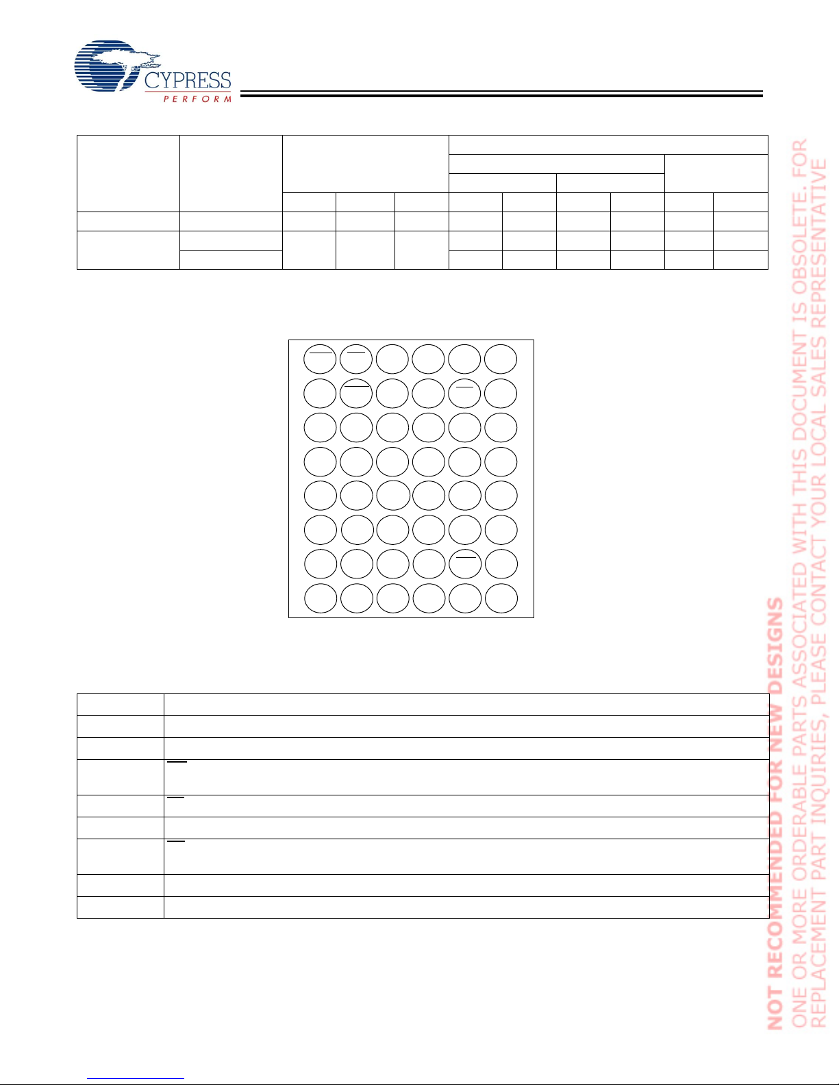
Pin Configurations
[2, 3, 4]
FBGA (Top View)
326541
CE
BLE
I/O
A
OE
BHE
8
0
A
3
A
A
1
A
CE
4
2
2
I/O
1
A
B
0
Standby (I
µAf = 1 MHz f = f
[2]
SB2
Max.
)
I/O
V
V
I/O
I/O
A
SS
CC
A
I/O
10
9
I/O
11
I/O
12
I/O
13
14
NC
15
A
8
18
5
A
17
DNU
A
14
A
12
A
9
A
6
A
7
A
16
A
15
A
13
A
10
I/O
I/O
I/O
I/O
WE
A
I/O
1
V
CC
3
V
SS
4
I/O
5
I/O
NC
11
C
2
D
E
F
6
G
7
H
Pin Definitions
Name Definition
Input A
Input/Output I/O0-I/O15. Data lines. Used as input or output lines depending on operation
Input/Control WE
Input/Control CE
Input/Control CE
Input/Control OE
Ground Vss. Ground for the device
Power Supply Vcc. Power supply for the device
. Address Inputs
0-A18
. Write Enable, Active LOW . When selected LOW, a WRITE is conducted. When selected HIGH, a READ is
conducted.
. Chip Enable 1, Active LOW.
1
. Chip Enable 2, Active HIGH.
2
. Output Enable, Active LOW. Controls the direction of the I/O pins. When LOW, the I/O pins behave as
outputs. When deasserted HIGH, I/O pins are three-stated, and act as input data pins
Notes:
2. Typical values are included for reference only and are not guaranteed or tested. Typical values are measured at V
3. NC pins are not connected on the die.
4. E3 (DNU) can be left as NC or V
to ensure proper application.
SS
Document #: 38-05014 Rev. *F Page 2 of 13
CC
= V
CC(typ.)
, TA = 25°C.
[+] Feedback
Page 3

CY62157CV30/33
Maximum Ratings
(Above which the useful life may be impaired. For user guidelines, not tested.)
Storage Temperature................................. –65°C to +150°C
Ambient Temperature with
Power Applied.............................................–55°C to +125°C
Supply Voltage to Ground Potential...–0.5V to V
DC Voltage Applied to Outputs
in High-Z State
DC Input Voltage
[5]
....................................–0.5V to VCC + 0.3V
[5]
.................................–0.5V to VCC + 0.3V
ccmax
+ 0.5V
Output Current into Outputs (LOW).............................20 mA
Electrical Characteristics Over the Operating Range
Parameter Description Test Conditions
V
V
V
V
I
IX
I
OZ
I
CC
I
SB1
I
SB2
OH
OL
IH
IL
Output HIGH Voltage IOH = –1.0 mA VCC = 2.7V 2.4 V
Output LOW Voltage IOL = 2.1 mA VCC = 2.7V 0.4 V
Input HIGH Voltage 2.2 VCC + 0.3V V
Input LOW Voltage –0.3 0.8 V
Input Leakage
Current
Output Leakage
GND < VI < V
CC
GND < VO < VCC, Output Disabled –10 +10 µA
Current
VCC Operating
Supply
Current
Automatic CE
Power-Down
Current— CMOS
Inputs
Automatic CE
Power-Down
Current—CMOS
Inputs
f = f
MAX
= 1/t
RC
f = 1 MHz 1.5 3
CE1 > VCC – 0.2V or CE2 < 0.2V
V
> VCC – 0.2V or VIN < 0.2V,
IN
(Address and Data Only),
f = f
max
f=0 (OE
, WE, BHE and BLE)
CE1 > VCC – 0.2V or CE2 < 0.2V
V
> VCC – 0.2V or VIN < 0.2V,
IN
f = 0, V
CC
= 3.3V
Static Discharge Voltage.......................................... > 2001V
(per MIL-STD-883, Method 3015)
Latch-up Current ........................................... .. ... ... > 200 mA
Operating Range
Ambient
Device Range
Temperature
CY62157CV30 Automotive-E –40°C to +125°C 2.7V – 3.3V
CY62157CV33 Automotive-A –40°C to +85°C 3.0V – 3.6V
Automotive-E –40°C to +125°C
CY62157CV30-70
–10 +10 µA
VCC = 3.3V
= 0 mA
I
OUT
CMOS Levels
[6]
[TA]
[2]
Max.
V
CC
UnitMin. Typ.
715mA
870µA
870µA
Notes:
5. V
6. T
= –2.0V for pulse durations less than 20 ns.
IL(min.)
is the “Instant-On” case temperature.
A
Document #: 38-05014 Rev. *F Page 3 of 13
[+] Feedback
Page 4

CY62157CV30/33
Electrical Characteristics Over the Operating Range
CY62157CV33-70
[2]
Parameter Description T est Conditions
V
OH
V
OL
V
IH
V
IL
I
IX
I
OZ
I
CC
Output HIGH
Voltage
Output LOW
Voltage
Input HIGH Voltage 2.2 VCC + 0.3V V
Input LOW Voltage –0. 3 0.8 V
Input Leakage
Current
Output Leakage
Current
VCC Operating
Supply
Current
IOH = –1.0 mA
V
= 3.0V
CC
2.4 V
IOL = 2.1 mA
V
= 3.0V
CC
GND < VI < V
CC
Auto-A –1 +1 µA
Auto-E –10 +10 µA
GND < VO < VCC, Output Disabled Auto-A –1 +1 µA
Auto-E –10 +10 µA
f = f
MAX
= 1/t
RC
VCC = 3.6V
= 0 mA
I
OUT
CMOS Levels
f = 1 MHz Auto-A/
Auto-A 5.5 12 mA
Auto-E 7 15
1.5 3
Auto-E
I
SB1
Automatic CE
Power-Down
Current—CMOS
Inputs
CE1 > VCC – 0.2V or
CE
< 0.2V
2
V
> VCC – 0.2V or
IN
< 0.2V,
V
IN
f = f
(Address and Data
max
Only),
Auto-A 10 30 µA
Auto-E 10 80 µA
f = 0 (OE,WE,BHE,and BLE)
I
SB2
Automatic CE
Power-Down
Current—CMOS
Inputs
Thermal Resistance
CE1 > VCC – 0.2V or
CE
< 0.2V
2
V
> VCC – 0.2V or
IN
< 0.2V,
V
IN
f = 0, V
[7]
CC
= 3.6V
Auto-A 10 30 µA
Auto-E 10 80 µA
Parameter Description Test Conditions FBGA Unit
Θ
JA
Θ
JC
Thermal Resistance
(Junction to Ambient)
Thermal Resistance
(Junction to Case)
Still Air, soldered on a 3 x 4.5 inch, two-layer printed
circuit board
Max.
0.4 V
55 °C/W
16 °C/W
UnitMin. Typ.
Note:
7. Tested initially and after any design or process ch anges that may affect these parameters.
Document #: 38-05014 Rev. *F Page 4 of 13
[+] Feedback
Page 5

CY62157CV30/33
Capacitance
[7]
Parameter Description Test Conditions Max. Unit
C
IN
C
OUT
Input Capacitance TA = 25°C, f = 1 MHz,
Output Capacitance 8 pF
AC Test Loads and Waveforms
R1
V
CC
OUTPUT
30 pF
INCLUDING
JIG AND
SCOPE
Parameters 3.0V 3.3V Unit
R1 1.105 1.216 ΚΩ
R2 1.550 1.374 ΚΩ
R
TH
V
TH
Equivalent to: THÉVENIN EQUIVALENT
= V
V
CC
CC(typ.)
VCC Typ
R
10%
TH
R2
GND
Rise TIme: 1 V/ns Fall Time: 1 V/ns
OUTPUT V
ALL INPUT PULSES
90%
TH
90%
10%
0.645 0.645 ΚΩ
1.75 1.75 V
6pF
Data Retention Characteristics (Over the Operating Range)
Parameter Description Conditions Min. Typ.
V
DR
I
CCDR
[8]
t
CDR
[8]
t
R
Data Retention Waveform
CE1 or
BHE.BLE
Notes:
8. Full Device AC operation requires linear V
.BLE is the AND of both BHE and BLE. Chip can be deselected by either disabling the chip enable signals or by disabling both BHE and BLE.
9. BHE
VCC for Data Retention 1.5 V
Data Retention Current V
Chip Deselect to Data
= 1.5V, CE1 > VCC – 0.2V or
CC
CE
< 0.2V,
2
V
> VCC – 0.2V or VIN < 0.2V
IN
Auto-A 4 20 µA
Auto-E
0ns
Retention Time
Operation Recovery Time t
[9]
DATA RETENTION MODE
V
CC
or
CE
2
V
ramp from V
CC
CC(min.)
t
CDR
DR
to V
CC(min.)
VDR> 1.5 V
> 100 µs or stable at V
CC(min.)
>100 µs.
V
CC(min.)
t
RC
R
[2]
Max. Unit
460µA
ns
Document #: 38-05014 Rev. *F Page 5 of 13
[+] Feedback
Page 6

CY62157CV30/33
Switching Characteristics Over the Operating Range
Parameter Description
Read Cycle
t
RC
t
AA
t
OHA
t
ACE
t
DOE
t
LZOE
t
HZOE
t
LZCE
t
HZCE
t
PU
t
PD
t
DBE
[11]
t
LZBE
t
HZBE
Write Cycle
t
WC
t
SCE
t
AW
t
HA
t
SA
t
PWE
t
BW
t
SD
t
HD
t
HZWE
t
LZWE
[14]
Read Cycle Time 70 ns
Address to Data Valid 70 ns
Data Hold from Address Change 10 ns
CE1 LOW and CE2 HIGH to Data Valid 70 ns
OE LOW to Data Valid 35 ns
OE LOW to Low-Z
OE HIGH to High-Z
[11]
[11, 12]
CE1 LOW and CE2 HIGH to Low-Z
CE1 HIGH or CE2 LOW to High-Z
CE1 LOW and CE2 HIGH to Power-up 0 ns
CE1 HIGH or CE2 LOW to Power-down 70 ns
BHE/BLE LOW to Data Valid 70 ns
BHE/BLE LOW to Low-Z
BHE/BLE HIGH to High-Z
[13]
[11, 12]
Write Cycle Time 70 ns
CE1 LOW and CE2 HIGH to Write End 60 ns
Address Set-up to Write End 60 ns
Address Hold from Write End 0 ns
Address Set-up to Write Start 0 ns
WE Pulse Width 50 ns
BHE/BLE Pulse Width 60 ns
Data Set-up to Write End 30 ns
Data Hold from Write End 0 ns
WE LOW to High-Z
WE HIGH to Low-Z
[11, 12]
[11]
[10]
[11]
[11, 12]
70 ns
UnitMin. Max.
5ns
25 ns
10 ns
25 ns
5ns
25 ns
25 ns
5ns
Notes:
10.Test conditions assume signal transition time of 5 ns or less, timing reference levels of V
specified I
11.At any given temperature and voltage condition, t
given device.
, t
12.t
HZOE
13.When both byte enables are toggled together this value is 10 ns.
14.The internal Write time of the memory is defined by the overlap of WE
Write and any of these signals can terminate a Write by going INACTIVE. The data input set-up and hold timing should be referenced to the edge of the signal
that terminates the Write.
and 30-pF load capacitance.
OL/IOH
, t
HZBE
, and t
HZCE
transitions are measured when the outputs enter a high-impedance state.
HZWE
Document #: 38-05014 Rev. *F Page 6 of 13
is less than t
HZCE
/2, input pulse levels of 0 to V
CC(typ.)
, t
LZCE
is less than t
HZBE
, CE1 = VIL, BHE and/or BLE = VIL, CE2 = VIH. All signals must be ACTIVE to initiate a
LZBE
, t
HZOE
is less than t
LZOE
, and t
, and output loading of the
CC(typ.)
is less than t
HZWE
LZWE
for any
[+] Feedback
Page 7

Switching Waveforms
Read Cycle No. 1 (Address Transition Controlled)
ADDRESS
t
OHA
DATA OUT PREVIOUS DATA VALID
t
AA
[15, 16]
CY62157CV30/33
t
RC
DATA VALID
Read Cycle No. 2 (OE Controlled)
ADDRESS
CE
1
CE
2
OE
BHE/BLE
t
LZBE
DATA OUT
V
CC
SUPPLY
CURRENT
HIGH IMPEDANCE
t
LZCE
t
PU
[16, 17]
t
ACE
t
LZOE
t
DOE
50%
t
RC
DATA VALID
t
HZOE
t
HZBE
t
HZCE
HIGH
IMPEDANCE
t
PD
I
CC
50%
I
SB
Notes:
15.Device is continuously selected. OE
is HIGH for Read cycle.
16.WE
17.Address valid prior to or coincident with CE
, CE1 = VIL, BHE and/or BLE = VIL, CE2 = VIH.
Document #: 38-05014 Rev. *F Page 7 of 13
, BHE, BLE transition LOW and CE2 transition HIGH.
1
[+] Feedback
Page 8

Switching Waveforms (continued)
Write Cycle No. 1 (WE Controlled)
ADDRESS
CE
1
CE
2
[14, 18, 19]
t
SCE
t
WC
CY62157CV30/33
t
AW
t
SA
WE
t
BHE/BLE
BW
OE
DATA I/O
Notes:
18.Data I/O is high-impedance if OE
goes HIGH or CE2 goes LOW simultaneously with WE HIGH, the output remains in a high-impedance state.
19.If CE
1
20.During this period, the I/Os are in output state and input signals should not be applied.
NOTE
20
= VIH.
t
HZOE
DATA
t
PWE
t
SD
IN
VALID
t
HA
t
HD
Document #: 38-05014 Rev. *F Page 8 of 13
[+] Feedback
Page 9

Switching Waveforms (continued)
Write Cycle No. 2 (CE1 or CE2 Controlled)
ADDRESS
CE
1
CE
2
WE
BHE/BLE
[14, 18, 19]
t
SA
t
AW
t
WC
CY62157CV30/33
t
SCE
t
HA
t
PWE
t
BW
OE
DATA I/O
NOTE
20
t
HZOE
Write Cycle No. 3 (WE Controlled, OE LOW)
ADDRESS
CE
1
CE
2
BHE/BLE
t
SA
WE
[19]
t
SD
IN
VALID
DATA
t
WC
t
SCE
t
BW
t
AW
t
PWE
t
HD
t
HA
DATAI/O
NOTE 20
Document #: 38-05014 Rev. *F Page 9 of 13
t
HZWE
t
SD
DATAIN VALID
t
LZWE
t
HD
[+] Feedback
Page 10

Switching Waveforms (continued)
Write Cycle No. 4 (BHE/BLE Controlled, OE LOW)
ADDRESS
CE
1
CE
2
BHE/BLE
t
SA
WE
CY62157CV30/33
[19]
t
WC
t
SCE
t
AW
t
BW
t
PWE
t
HA
t
HD
DATA I/O
NOTE 20
t
SD
DATA
IN
VALID
Truth Table
CE
H X X X X X High Z Deselect/Power-Down Standby (I
X L X X X X High Z Deselect/Power-Down Standby (I
X X X X H H High Z Deselect/Power-Down Standby (ISB)
CE
1
L H H L L L Data Out (I/O
L H H L H L Data Out (I/O
L H H L L H Data Out (I/O
WE OE BHE BLE Inputs/Outputs Mode Power
2
–I/O15) Read Active (ICC)
O
–I/O
I/O
8
15
I/O
–I/O7 in High Z
0
–I/O7);
O
in High Z
–I/O15);
8
Read Active (I
Read Active (I
L H H H L L High Z Output Disabled Active (I
L H H H H L High Z Output Disabled Active (I
L H H H L H High Z Output Disabled Active (I
L H L X L L Data In (I/O
L H L X H L Data In (I/O
I/O
–I/O
8
L H L X L H Data In (I/O
I/O
–I/O7 in High Z
0
–I/O15) Write Active (ICC)
O
O
in High Z
15
–I/O15);
8
–I/O7);
Write Active (I
Write Active (I
CC
CC
CC
CC
CC
CC
CC
SB
SB
)
)
)
)
)
)
)
)
)
Document #: 38-05014 Rev. *F Page 10 of 13
[+] Feedback
Page 11

Typical DC and AC Characteristics
[2]
CY62157CV30/33
14.0
MoBL
12.0
10.0
(mA)
8.0
CC
I
6.0
4.0
2.0
0.0
2.2
2.5
SUPPLY VOLTAGE (V)
12.0
10.0
MoBL
8.0
SB (µA)
I
6.0
4.0
2.0
0
2.2
2.5
2.7
SUPPLY VOLTAGE (V)
(f = f
(f = 1 MHz)
2.7
Operating Current vs. Supply Voltage
14.0
MoBL
12.0
10.0
(mA)
8.0
CC
max
, 70ns)
I
6.0
(f = f
4.0
2.0
0.0
2.7
3.0
(f = 1 MHz)
3.3
SUPPLY VOLTAGE (V)
Standby Current vs. Supply Voltage
12.0
10.0
MoBL
8.0
SB (µA)
I
6.0
4.0
2.0
0
3.3
3.0
2.7
SUPPLY VOLTAGE (V)
Access Time vs. Supply Voltage
max
, 70ns)
14.0
MoBL
12.0
10.0
(mA)
8.0
CC
I
6.0
4.0
2.0
0.0
3.3
3.0
SUPPLY VOLTAGE (V)
12.0
MoBL
10.0
8.0
SB (µA)
I
6.0
4.0
2.0
0
3.3
3.0
SUPPLY VOLTAGE (V)
(f = f
(f = 1 MHz)
3.6
3.6
max
, 70ns)
60
MoBL
50
40
30
AA (ns)
20
T
10
0
2.2
2.5
2.7
SUPPLY VOLTAGE (V)
60
MoBL
50
40
30
AA (ns)
20
T
10
0
3.0
2.7
3.3
SUPPLY VOLTAGE (V)
60
MoBL
50
40
30
AA (ns)
20
T
10
0
3.0
3.3
SUPPLY VOLTAGE (V)
3.6
Document #: 38-05014 Rev. *F Page 11 of 13
[+] Feedback
Page 12

CY62157CV30/33
Ordering Information
Speed
(ns) Ordering Code
70 CY62157CV30LL-70BAE 51-85128 48-Ball (6 mm x 10 mm x 1.2 mm) FBGA Automotive-E
CY62157CV33LL-70BAXA Automotive-A
CY62157CV33LL-70BAE Automotive-E
Package Diagram
Package
Diagram Package Type
48-Ball (6 mm x 10 mm x 1.2 mm) FBGA (51-85128)
Operating
Range
A
0.25 C
10.00±0.10
B
0.53±0.05
A
B
C
D
E
F
G
H
A1 CORNER
TOP VIEW
6.00±0.10
BOTTOM VIEW
A1 CORNER
Ø0.05 M C
Ø0.25 M C A B
Ø0.30±0.05(48X)
465231
0.75
5.25
10.00±0.10
A
B
0.15(4X)
0.21±0.05
0.15 C
65
2.625
1.875
6.00±0.10
0.75
3.75
234
1
A
B
C
D
E
F
G
H
SEATING PLANE
C
0.36
MoBL, MoBL2, and More Battery Life are trademarks of Cypress Semiconducto r Corporation. All product and company names
mentioned in this document may be the trademarks of their respective holders.
Document #: 38-05014 Rev. *F Page 12 of 13
© Cypress Semiconductor Corporation, 2006. The information contained herein is subject to ch ange without notice. Cypress Semiconductor Corporation assumes no resp onsib ility for the u se
of any circuitry other than circuitry embodied in a Cypress product. Nor does it convey or imply any license under patent or other rights. Cypress products are not warranted nor intended to be
used for medical, life support, life saving, critical control or safety applications, unless pursuant to an express written agreement with Cypress. Furtherm ore, Cypress do es not authori ze its
products for use as critical components in life-support systems where a malfunction or failure may reasonably be expected to result in significant injury to the user. The inclusion of Cypress
products in life-support systems application implies that the manufacturer assumes all risk of such use and in doing so indemnifies Cypress against all charges.
51-85128-*D
1.20 MAX
[+] Feedback
Page 13

CY62157CV30/33
Document History Page
Document Title: CY62157CV30/33 512K x 16 Static RAM
Document Number: 38-05014
REV. ECN NO. Issue Date
** 106184 05/10/01 HRT/MGN New data sheet – Advance Information
*A 107241 07/24/01 MGN Made corrections to Advance Information
*B 109621 03/11/02 MGN Changed from Advance Information to Final
*C 114218 05/01/02 GUG/MGN Improved Typical and Max I
*D 238448 See ECN AJU Added Automotive Product Information
*E 269729 See ECN SYT Added Automotive Product information for CY62157CV30 – 70 ns
*F 498575 See ECN NXR Removed Industrial Operating Range
Orig. of
Change Description of Change
Added 55 ns bin
values
CC
Added I
Removed 55 ns speed bin
Removed CY62157CV25 part number from the Product Offering
Added Automotive-A operating range
Updated the Ordering Information Table
IX
and I
values for Automotive range of CY62157CV33 – 70 ns
OZ
Document #: 38-05014 Rev. *F Page 13 of 13
[+] Feedback
 Loading...