

Page 1

CY62146ESL MoBL
®
4-Mbit (256K x 16) Static RAM
Features
256K x 16
RAM Array
IO
0
–IO
7
ROW DECODER
A
8
A
7
A
6
A
5
A
2
COLUMN DECODER
A
11
A12A
13
A
14
A
15
SENSE AMPS
DATA IN DRIVERS
OE
A
4
A
3
IO8–IO
15
CE
WE
BHE
A
16
A
0
A
1
A
9
A
10
BLE
A
17
■ Very high speed: 45 ns
■ Wide voltage range: 2.2V–3.6V
■ Ultra low standby power
❐ Typical Standby current: 1 μA
❐ Maximum Standby current: 7 μA
■ Ultra low active power
❐ Typical active current: 2 mA at f = 1 MHz
■ Easy memory expansion with CE and OE features
■ Automatic power down when deselected
■ CMOS for optimum speed and power
■ Available in Pb-free 44-pin TSOP II package
and 4.5V–5.5V
Functional Description
The CY62146ESL is a high performance CMOS static RAM
organized as 256K words by 16 bits. This device features
advanced circuit design to provide ultra low active current. This
is ideal for providing More Battery Life™ (MoBL
®
) in portable
applications such as cellular telephones. The device also has an
automatic power down feature that reduces power consumption
when addresses are not toggling. Placing the device into standby
Logic Block Diagram
mode reduces power consumption by more than 99% when
deselected (CE
) are placed in a high impedance state when:
IO
15
■ Deselected (CE HIGH)
■ Outputs are disabled (OE HIGH)
■ Both Byte High Enable and Byte Low Enable are disabled
(BHE
, BLE HIGH)
■ Write operation is active (CE LOW and WE LOW)
To write to the device, take Chip Enable (CE
(WE
) inputs LOW. If Byte Low Enable (BLE) is LOW, then data
from IO pins (IO
specified on the address pins (A
Enable (BHE
HIGH). The input and output pins (IO0 through
) and Write Enable
through IO7) is written into the location
0
) is LOW, then data from IO pins (IO8 through IO15)
through A17). If Byte High
0
is written into the location specified on the address pins (A
through A17).
To read from the device, take Chip Enable (CE
Enable (OE
Byte Low Enable (BLE
) LOW while forcing the Write Enable (WE) HIGH. If
) is LOW, then data from the memory
location specified by the address pins appea rs on IO
Byte High Enable (BHE
appears on IO
complete description of read and write modes.
to IO15. See the “Truth Table” on page 10 for a
8
) is LOW, then data from memory
) and Output
to IO7. If
0
For best practice recommendations, refer to the Cypress
application note AN1064, SRAM System Guidelines.
0
Cypress Semiconductor Corporation • 198 Champion Court • San Jose, CA 95134-1709 • 408-943-2600
Document #: 001-43142 Rev. ** Revised January 04, 2008
[+] Feedback [+] Feedback
Page 2

CY62146ESL MoBL
®
Pin Configuration
1
2
3
4
5
6
7
8
9
11
14
31
32
36
35
34
33
37
40
39
38
12
13
41
44
43
42
16
15
29
30
A
5
18
17
20
19
27
28
25
26
22
21
23
24
A
6
A
7
A
4
A
3
A
2
A
1
A
0
A
15
A
16
A
8
A
9
A
10
A
11
A
13
A
14
A
12
OE
BHE
BLE
CE
WE
IO
0
IO
1
IO
2
IO
3
IO
4
IO
5
IO
6
IO
7
IO
8
IO
9
IO
10
IO
11
IO
12
IO
13
IO
14
IO
15
V
CC
V
CC
V
SS
V
SS
NC
10
A
17
Notes
1. NC pins are not connected on the die.
2. Datasheet specifications are not guaranteed for V
CC
in the range of 3.6V to 4.5V.
3. Typical values are included for reference only and are not guaranteed or tested. Typical values are measured at V
CC
= 3V, and VCC = 5V, TA = 25°C.
Figure 1. 44-Pin TSOP II (Top View)
[1]
Product Portfolio
Product Range VCC Range (V)
[2]
CY62146ESL Industrial 2.2V–3.6V and 4.5V–5.5V 45 2 2.5 15 20 1 7
Document #: 001-43142 Rev. ** Page 2 of 12
Speed
(ns)
Typ
Power Dissipation
Operating ICC, (mA)
f = 1MHz f = f
[3]
Max Typ
max
[3]
Max Typ
Standby, I
(μA)
[3]
SB2
Max
[+] Feedback [+] Feedback
Page 3

CY62146ESL MoBL
®
Maximum Ratings
Notes
4. V
IL
(min) = –2.0V for pulse durations less than 20 ns.
5. V
IH
(max) = VCC + 0.75V for pulse durations less than 20 ns.
6. Full Device AC operation assumes a 100 μs ramp time from 0 to V
CC
(min) and 200 μs wait time after VCC stabilization.
Exceeding the maximum ratings may impair the useful life of the
device. These user guidelines are not tested.
Storage Temperature.................................. –65°C to +150°C
Ambient Temperature with
Output Current into Outputs (LOW).............................20 mA
Static Discharge Voltage............................................>2001V
(MIL-STD-883, Method 3015)
Latch up Current............................................... .......>200 mA
Operating Range
Power Applied ............................................–55°C to +125°C
Supply Voltage to Ground Potential..................–0.5V to 6.0V
DC Voltage Applied to Outputs
in High-Z State
DC Input Voltage
[4, 5]
...........................................–0.5V to 6.0V
[4, 5]
........................................–0.5V to 6.0V
Electrical Characteristics
Over the Operating Range
Parameter Description Test Conditions
V
V
V
V
I
IX
I
OZ
I
CC
I
SB1
I
SB2
OH
OL
IH
IL
Output HIGH Voltage 2.2 < VCC < 2.7 IOH = –0.1 mA 2.0 V
2.7 <
VCC < 3.6 IOH = –1.0 mA 2.4
4.5 <
VCC < 5.5 IOH = –1.0 mA 2.4
Output LOW Voltage 2.2 < VCC < 2.7 IOL = 0.1 mA 0.4 V
2.7 <
VCC < 3.6 IOL = 2.1mA 0.4
4.5 <
VCC < 5.5 IOL = 2.1mA 0.4
Input HIGH Voltage 2.2 < VCC < 2.7 1.8 V
2.7 <
VCC < 3.6 2.2 V
4.5 <
VCC < 5.5 2.2 V
Input LOW Voltage 2.2 < VCC < 2.7 –0.3 0.6 V
2.7 <
VCC < 3.6 –0.3 0.8
4.5 <
VCC < 5.5 –0.5 0.8
Input Leakage Current GND < VI < V
CC
Output Leakage Current GND < VO < VCC, Output Disabled –1 +1 μA
VCC Operating Supply
Current
Automatic CE Power
down Current — CMOS
Inputs
Automatic CE Power
down Current — CMOS
f = f
= 1/t
max
RC
f = 1 MHz 2 2.5
CE
> V
− 0.2V, V
CC
f = f
f = 0 (OE
CE
f = 0, V
(Address and Data Only),
max
, BHE, BLE and WE),
> VCC – 0.2V, VIN > VCC – 0.2V or VIN < 0.2V,
=
CC
V
CC(max)
IN
>
V
VCC = V
I
OUT
– 0.2V or V
CC
Inputs
Device Range
Ambient
Temperature
[6]
V
CC
CY62146ESL Industrial –40°C to +85°C 2.2V–3.6V,
and
4.5V–5.5V
45 ns
[3]
Max
+ 0.3 V
CC
+ 0.3
CC
+ 0.5
CC
UnitMin Typ
–1 +1 μA
CCmax
15 20 mA
= 0 mA, CMOS levels
< 0.2V,
IN
= V
V
CC
CC(max)
17μA
17μA
Document #: 001-43142 Rev. ** Page 3 of 12
[+] Feedback [+] Feedback
Page 4

CY62146ESL MoBL
®
Capacitance
VCC
V
CC
OUTPUT
R2
30 pF
INCLUDING
JIG AND
SCOPE
GND
90%
10%
90%
10%
Rise Time = 1 V/ns
Fall Time = 1 V/ns
OUTPUT V
Equivalent to: THÉ VENIN EQUIVALENT
ALL INPUT PULSES
R
TH
R1
TH
Tested initially and after any design or process changes that may affect these parameters.
Parameter Description Test Conditions Max Unit
C
C
IN
OUT
Input Capacitance TA = 25°C, f = 1 MHz,
= V
V
CC
Output Capacitance 10 pF
CC(typ)
10 pF
Thermal Resistance
Tested initially and after any design or process changes that may affect these parameters.
Parameter Description Test Conditions TSOP II Unit
Θ
Θ
Thermal Resistance
JA
(Junction to Ambient)
Thermal Resistance
JC
(Junction to Case)
Still Air, soldered on a 3 × 4.5 inch, two-layer
printed circuit board
77 °C/W
13 °C/W
AC Test Loads and Waveforms
Parameters 2.5V 3.0V 5.0V Unit
R1 16667 1103 1800 Ω
R2 15385 1554 990 Ω
R
V
TH
TH
8000 645 639 Ω
1.20 1.75 1.77 V
Document #: 001-43142 Rev. ** Page 4 of 12
[+] Feedback [+] Feedback
Page 5
CY62146ESL MoBL
®
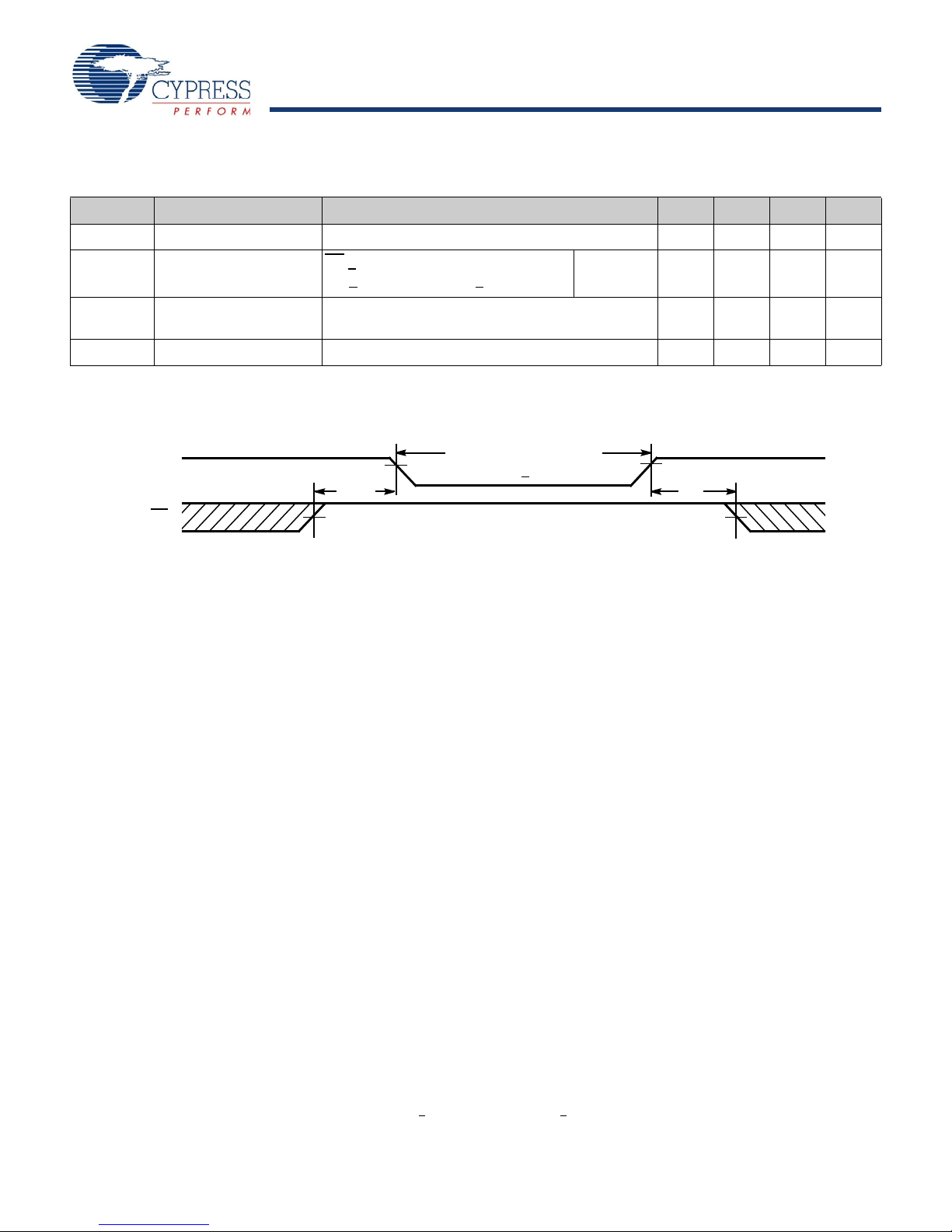
Data Retention Characteristics
Notes
7. T ested initially and after any design or process changes that may affect these parameters.
8. Full device operation requires linear V
CC
ramp from V
DR
to V
CC(min)
> 100 μs or stable at V
CC(min)
> 100 μs.
V
CC(min)
V
CC(min)
t
CDR
VDR> 1.5V
DATA RETENTION MODE
t
R
V
CC
CE
Over the Operating Range
Parameter Description Conditions Min Typ
V
DR
I
CCDR
t
CDR
[8]
t
R
[7]
VCC for Data Retention 1.5 V
Data Retention Current
Chip Deselect to Data
> VCC – 0.2V,
V
> VCC – 0.2V or VIN < 0.2V
IN
= 1.5V 1 7 μA
V
CC
0ns
CE
Retention Time
Operation Recovery Time t
RC
Data Retention Waveform
[3]
Max Unit
ns
Document #: 001-43142 Rev. ** Page 5 of 12
[+] Feedback [+] Feedback
Page 6
CY62146ESL MoBL
®
Switching Characteristics
Notes
9. T est conditions for all p aramete rs other than tri-st ate p arameters assume signal tr ansition time of 3 ns or less, timing ref erence levels of 1.5V, input pulse levels of 0 to
3V, and output loading of the specified I
OL/IOH
as shown in the AC Test Loads and Waveforms on page 4 .
10.At any temperature and voltage condition, t
HZCE
is less than t
LZCE
, t
HZBE
is less than t
LZBE
, t
HZOE
is less than t
LZOE
, and t
HZWE
is less than t
LZWE
for any device.
11. t
HZOE
, t
HZCE
, t
HZBE
, and t
HZWE
transitions are measured when the outputs enter a high-impedance state.
12.The internal write time of the memory is defined by the overlap of WE
, CE = VIL, BHE, BLE or both = VIL. All signals must be active to initiate a write and any of th ese
signals can terminate a write by going inactive. The data input setup and hold timing must be referenced to the edge of the signal that terminates the write.
Over the Operating Range
Parameter Description
Read Cycle
t
RC
t
AA
t
OHA
t
ACE
t
DOE
t
LZOE
t
HZOE
t
LZCE
t
HZCE
t
PU
t
PD
t
DBE
t
LZBE
t
HZBE
Write Cycle
t
WC
t
SCE
t
AW
t
HA
t
SA
t
PWE
t
BW
t
SD
t
HD
t
HZWE
t
LZWE
Read Cycle Time 45 ns
Address to Data Valid 45 ns
Data Hold from Address Change 10 ns
CE LOW to Data Valid 45 ns
OE LOW to Data Valid 22 ns
OE LOW to LOW-Z
OE HIGH to High-Z
CE LOW to Low-Z
CE HIGH to High-Z
CE LOW to Power Up 0 ns
CE HIGH to Power Down 45 ns
BLE/BHE LOW to Data Valid 22 ns
BLE/BHE LOW to Low-Z
BLE/BHE HIGH to HIGH-Z
[12]
Write Cycle Time 45 ns
CE LOW to Write End 35 ns
Address Setup to Write End 35 ns
Address Hold from Write End 0 ns
Address Setup to Write Start 0 ns
WE Pulse Width 35 ns
BLE/BHE LOW to Write End 35 ns
Data Setup to Write End 25 ns
Data Hold from Write End 0 ns
WE LOW to High-Z
WE HIGH to Low-Z
[9]
[10]
[10, 1 1]
[10]
[10, 11]
[10]
[10, 11]
[10, 11]
[10]
45 ns
Min Max
Unit
5ns
18 ns
10 ns
18 ns
5ns
18 ns
18 ns
10 ns
Document #: 001-43142 Rev. ** Page 6 of 12
[+] Feedback [+] Feedback
Page 7
CY62146ESL MoBL
®
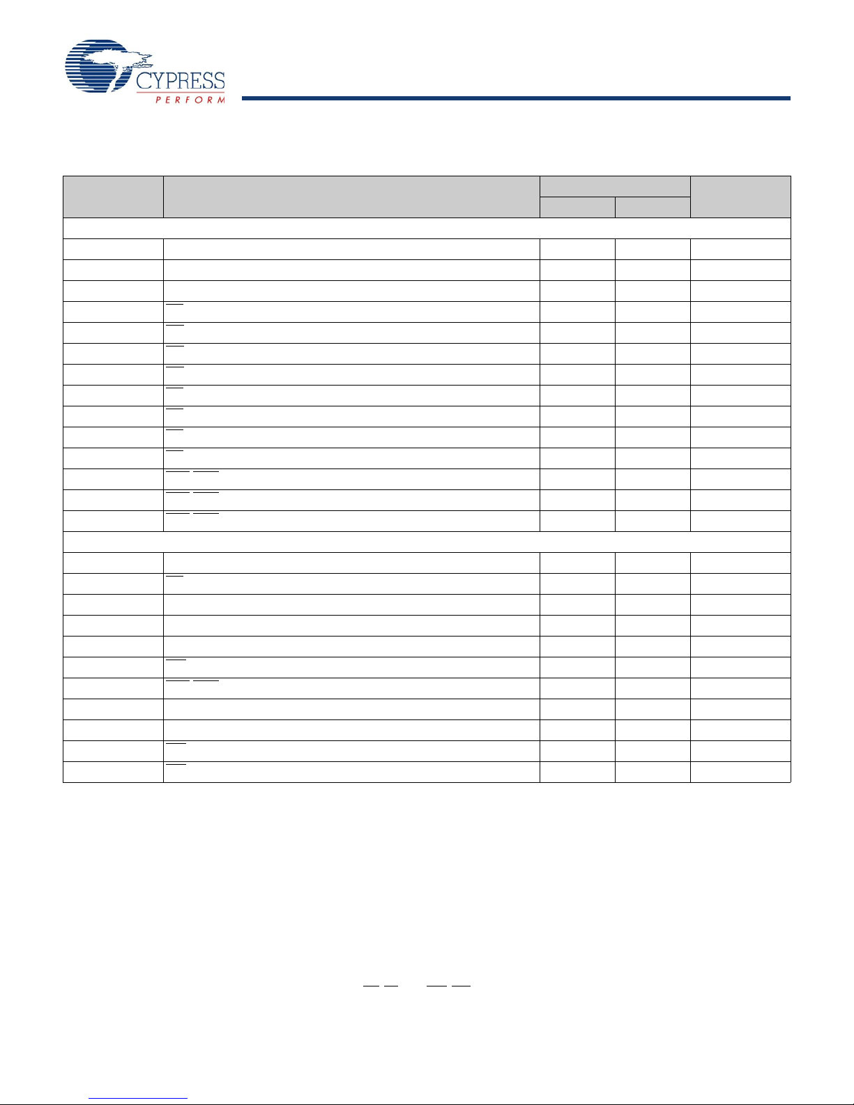
Switching Waveforms
PREVIOUS DATA VALID DATA VALID
RC
t
AA
t
OHA
t
RC
ADDRESS
DATA OUT
50%
50%
DATA VALID
t
RC
t
ACE
t
LZBE
t
LZCE
t
PU
HIGH IMPEDANCE
I
CC
t
HZOE
t
HZCE
t
PD
t
HZBE
t
LZOE
t
DBE
t
DOE
IMPEDANCE
HIGH
I
SB
DATA OUT
OE
CE
V
CC
SUPPLY
CURRENT
BHE
/BLE
ADDRESS
Notes
13.The device is continuously selected. OE
, CE = VIL, BHE, BLE, or both = VIL.
14.WE
is HIGH for read cycle.
15.Address valid before or similar to CE
, BHE, BLE transition LOW.
Figure 2. Read Cycle No.1: Address Transition Controlled.
[13, 14]
Figure 3. Read Cycle No. 2: OE Controlled
[14, 15]
Document #: 001-43142 Rev. ** Page 7 of 12
[+] Feedback [+] Feedback
Page 8

CY62146ESL MoBL
®
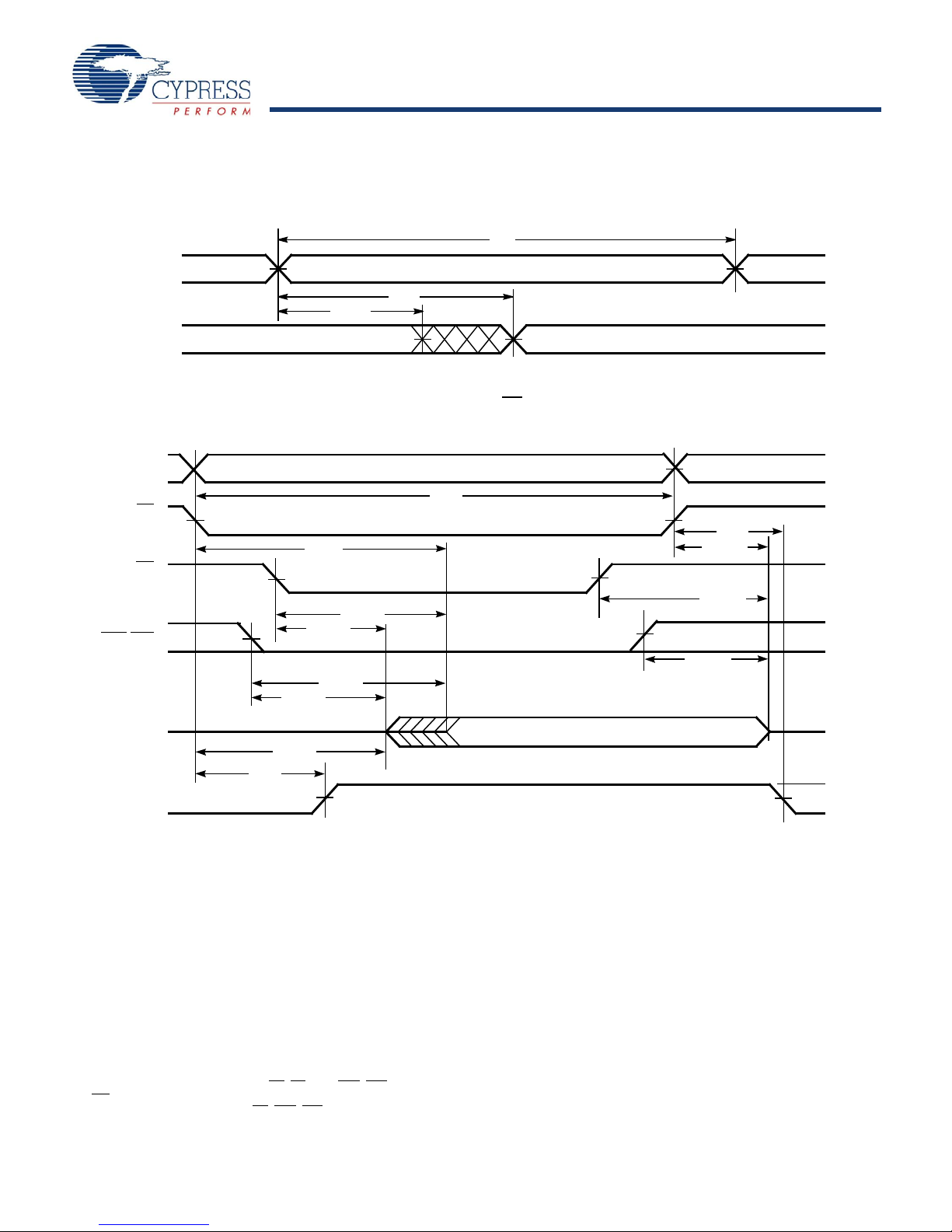
Switching Waveforms (continued)
t
HD
t
SD
t
PWE
t
SA
t
HA
t
AW
t
WC
t
HZOE
DATA
IN
NOTE 18
t
BW
t
SCE
DATA IO
ADDRESS
CE
WE
OE
BHE/BLE
t
HD
t
SD
t
PWE
t
HA
t
AW
t
SCE
t
WC
t
HZOE
DATA
IN
t
BW
t
SA
CE
ADDRESS
WE
DATA IO
OE
BHE/BLE
NOTE 18
Notes
16.Data IO is high impedance if OE
= VIH.
17.If CE
goes HIGH simultaneously with WE = VIH, the output remains in a high impedance state.
18.During this period, the IOs are in output state. Do not apply input signals.
Figure 4. Write Cycle No 1: WE
Controlled
[12, 16, 17]
Figure 5. Write Cycle 2: CE Controlled
[12, 16, 17]
Document #: 001-43142 Rev. ** Page 8 of 12
[+] Feedback [+] Feedback
Page 9
CY62146ESL MoBL
®
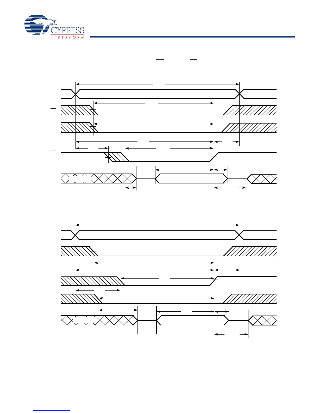
Switching Waveforms (continued)
DATAIN
t
HD
t
SD
t
LZWE
t
PWE
t
SA
t
HA
t
AW
t
SCE
t
WC
t
HZWE
t
BW
NOTE 18
CE
ADDRESS
WE
DATA IO
BHE
/BLE
t
HD
t
SD
t
SA
t
HA
t
AW
t
WC
DATA
IN
t
BW
t
SCE
t
PWE
t
HZWE
t
LZWE
NOTE 18
DATA IO
ADDRESS
CE
WE
BHE
/BLE
Figure 6. Write Cycle 3: WE
controlled, OE LOW
[17]
Figure 7. Write Cycle 4: BHE/BLE Controlled, OE LOW
Document #: 001-43142 Rev. ** Page 9 of 12
[17]
[+] Feedback [+] Feedback
Page 10

CY62146ESL MoBL
®
Truth Table
CE WE OE BHE BLE Inputs/Outputs Mode Power
H X X X X High-Z Deselect/Power down Standby (I
L X X H H High-Z Output Disabled Active (I
L H L L L Data Out (IO
LHLHLData Out (IO
IO
–IO
8
L H L L H Data Out (IO8–IO15);
IO
–IO7 in High-Z
0
–IO15) Read Active (ICC)
0
in High-Z
15
–IO7);
0
Read Active (I
Read Active (I
L H H L L High-Z Output Disabled Active (ICC)
L H H H L High-Z Output Disabled Active (I
L H H L H High-Z Output Disabled Active (I
L L X L L Data In (IO
L L X H L Data In (IO
–IO
IO
8
L L X L H Data In (IO
IO
–IO7 in High-Z
0
–IO15) Write Active (ICC)
0
0
in High-Z
15
8
–IO7);
–IO15);
Write Active (I
Write Active (I
Ordering Information
CC
CC
CC
CC
CC
CC
CC
SB
)
)
)
)
)
)
)
)
Speed
(ns)
Ordering Code
Package
Diagram
Package Type
Operating
Range
45 CY62146ESL-45ZSXI 51-85087 44-pin Thin Small Outline Package Type II (Pb-free) Industrial
Document #: 001-43142 Rev. ** Page 10 of 12
[+] Feedback [+] Feedback
Page 11
CY62146ESL MoBL
®
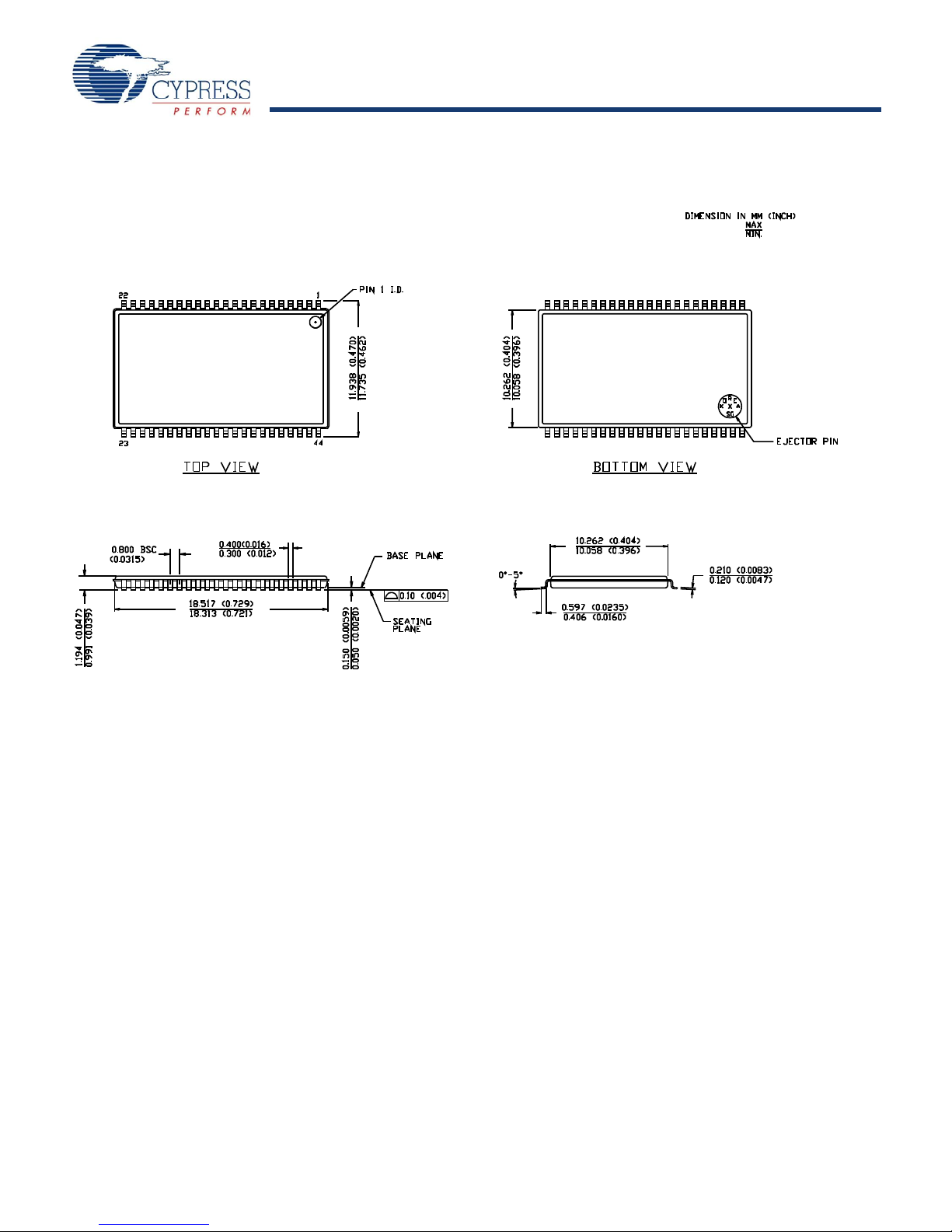
Package Diagrams
51-85087-*A
Figure 8. 44-Pin TSOP II, 51-85087
Document #: 001-43142 Rev. ** Page 11 of 12
[+] Feedback [+] Feedback
Page 12

CY62146ESL MoBL
®
Document History Page
Document Title: CY62146ESL MoBL® 4-Mbit (256K x 16) Static RAM
Document Number: 001-43142
REV. ECN NO. Issue Date
** 1875228 See ECN VKN/AESA New Data Sheet
Orig. of
Change Description of Change
© Cypress Semiconductor Corporation, 2008. The information contained herein is subject to change without notice. Cypress Semiconductor Corporation assumes no responsibility for the use of any
circuitry other than circuitry embodied in a Cypress product. Nor do es it convey or imply any l icense under pa tent or other right s. Cypress product s are not warrante d nor intended to be u sed for medical,
life support, life saving, critical control or safety applications, unless pursuant to an express written agreement with Cypress. Furthermore, Cypress does not authorize its products for use as critical
components in life-support systems where a malfunction or failure may reasonably be expected to result in significant injury to the user. The inclusion of Cypress products in life-support systems
application implies that the manufacturer assumes all risk of such use and in doing so indemnifies Cypress against all charges.
Any Source Code (software and/or firmware) is owned by Cypress Semiconductor Corporation (Cypress) and is protected by and subject to worldwide patent protection (United States and foreign),
United States co pyright la ws and inte rnatio na l tre aty prov isi ons. Cyp ress he reby g rant s to lice nsee a p erson al, no n-ex clusi ve, non-tra nsferable license to copy, use, modify , create de rivative works of ,
and compile the Cypress Source Code and derivative works for the sole purpo se of creating custom sof tware and or firm ware in support of licen see product to be use d only in conjunction with a Cypress
integrated circuit as specified in th e applicable agreement. Any reproductio n, modification, translation, co mpilation, o r representati on of this Sour ce Code except as specified above is prohibited without
the express written permission of Cypress.
Disclaimer: CYPRESS MAKES NO WARRANTY OF ANY KIND, EXPRESS OR IMPLIED, WITH REGARD TO THIS MATERIAL, INCLUDING, BUT NOT LIMITED TO, THE IMPLIED WARRANTIES
OF MERCHANTABILITY AND FITNESS FOR A PARTICULAR PURPOSE. Cypress reserves the right to make changes without further notice to the materials described herein. Cypress does not
assume any liability arising out of the ap plicati on or u se o f any pr oduct o r circui t descri bed h erein. Cypr ess does not aut horize it s product s for use a s critical compo nent s in life-support systems whe re
a malfunction or failure may reasonab ly be expected to resu lt in significant injury t o the user. The inclusion of Cypress’ prod uct in a life-support systems application implies that the manufacturer
assumes all risk of such use and in doing so indemnifies Cypress against all charges.
Use may be limited by and subject to the applicable Cypress software license agreement.
Document #: 001-43142 Rev. ** Revised January 04, 2008 Page 12 of 12
MoBL is a registered trademark and Mor e Battery Life is a trademark of Cypre ss Semiconductor. A ll product and company names mentioned in this document are the trademarks of their respective holders.
[+] Feedback [+] Feedback
 Loading...