

Page 1

MoBL
®
,CY62126EV30
1-Mbit (64K x 16) Static RAM
Features
Note
1. For best practice recommendations, refer to the Cypress application note AN1064, SRAM System Guidelines.
Logic Block Diagram
Functional Description
■ High speed: 45 ns
■ Temperature ranges
❐ Industrial: –40°C to +85°C
❐ Automotive: –40°C to +125°C
■ Wide voltage range: 2.2V to 3.6V
■ Pin compatible with CY62126DV30
■ Ultra low standby power
❐ Typical standby current: 1 μA
❐ Maximum standby current: 4 μA
■ Ultra low active power
❐ Typical active current: 1.3 mA at f = 1 MHz
■ Easy memory expansion with CE and OE features
■ Automatic power down when deselected
■ CMOS for optimum speed and power
■ Offered in Pb-free 48-ball VFBGA and 44-pin TSOP II
packages
The CY62126EV30 is a high performance CMOS static RAM
organized as 64K words by 16 bits
[1]
. This device features
advanced circuit design to provide ultra low active current. This
is ideal for providing More Battery Life™ (MoBL®) in portable
applications such as cellular telephones. The device also has an
automatic power down feature that significantly reduces power
consumption when addresses are not toggling. Placing the
device in standby mode reduces power consumption by more
than 99 percent when deselected (CE
output pins (IO
state when:
■ Deselected (CE HIGH)
■ Outputs are disabled (OE HIGH)
■ Both Byte High Enable and Byte Low Enable are disabled
(BHE
, BLE HIGH)
■ Write operation is active (CE LOW and WE LOW)
through IO15) are placed in a high impedance
0
HIGH). The input and
To write to the device, take Chip Enable (CE) and Write Enable
) inputs LOW. If Byte Low Enable (BLE) is LOW, then data
(WE
from IO pins (IO
specified on the address pins (A
Enable (BHE
through IO7) is written into the location
0
) is LOW, then data from IO pins (IO8 through IO15)
through A15). If Byte High
0
is written into the location specified on the address pins (A
through A15).
To read from the device, take Chip Enable (CE
Enable (OE
Byte Low Enable (BLE
) LOW while forcing the Write Enable (WE) HIGH. If
) is LOW, then data from the memory
location specified by the address pins appear on IO
Byte High Enable (BHE
appears on IO
complete description of read and write modes.
to IO15. See the “Truth Table” on page 9 for a
8
) is LOW, then data from memory
) and Output
to IO7. If
0
0
Cypress Semiconductor Corporation • 198 Champion Court • San Jose, CA 95134-1709 • 408-943-2600
Document #: 38-05486 Rev. *E Revised January 5, 2009
[+] Feedback
Page 2
MoBL
®
, CY62126EV30
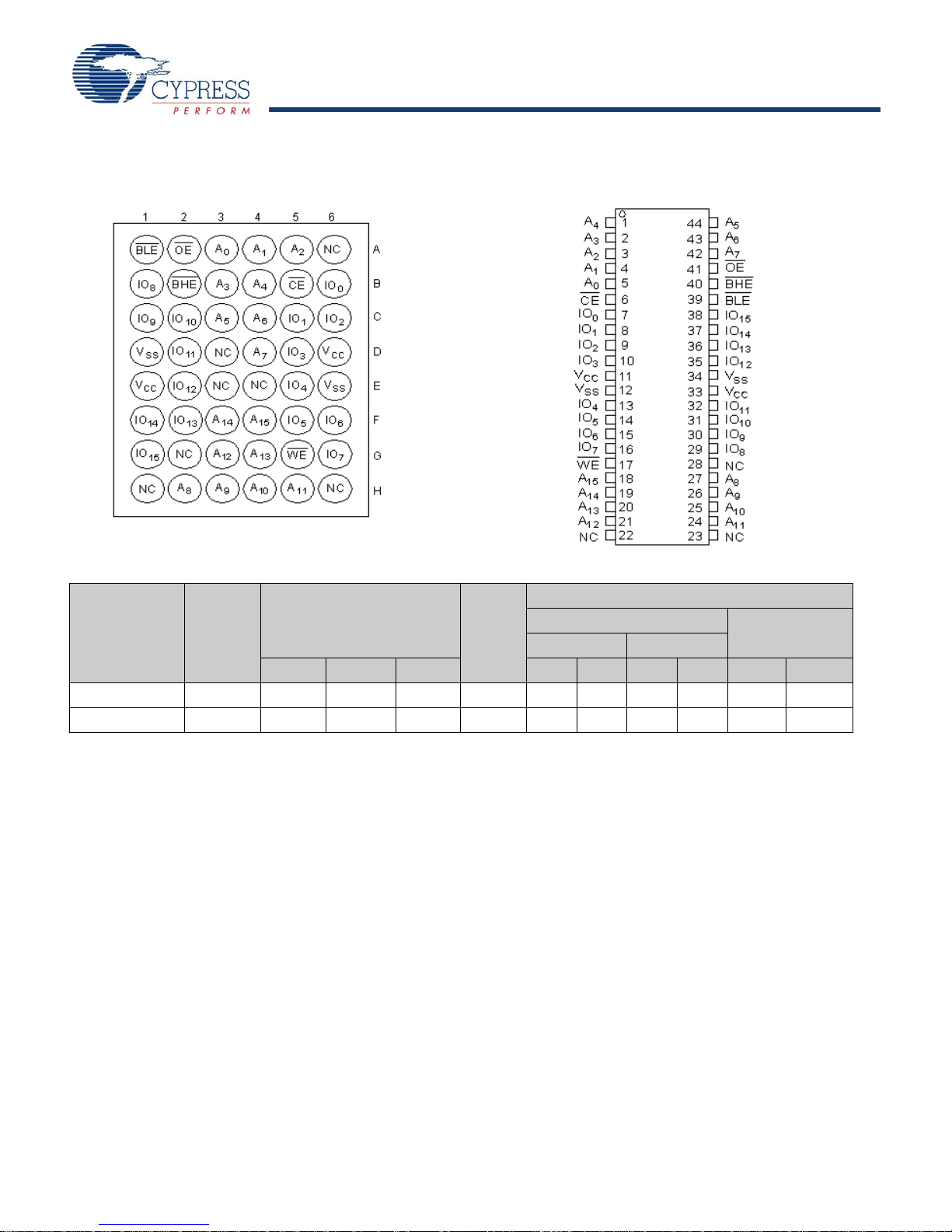
Pin Configurations
Notes
2. NC pins are not connected on the die.
3. Typical values are included for reference only and are not guaranteed or tested. Typical values are measured at V
CC
= V
CC(typ)
, TA = 25°C.
Figure 1. 44-Ball VFBGA (Top View) Figure 2. 44-Pin TSOP II (Top View)
Table 1. Product Portfolio
Power Dissipation
Product Range
VCC Range (V)
Min Typ
[3]
Speed
(ns)
Max Typ
Operating, I
CC
(mA)
f = 1 MHz f = f
[3]
Max Typ
[3]
CY62126EV30LL Industrial 2.2 3.0 3.6 45 1.3 2 11 16 1 4
CY62126EV30LL Automotive 2.2 3.0 3.6 55 1.3 4 11 35 1 30
[2]
max
Max Typ
Standby, I
[3]
SB2
Max
(μA)
Document #: 38-05486 Rev. *E Page 2 of 13
[+] Feedback
Page 3

MoBL
®
, CY62126EV30
Maximum Ratings
Notes
4. V
IL(min)
= –2.0V for pulse durations less than 20 ns.
5. V
IH(max)
= VCC+0.75V for pulse durations less than 20 ns.
6. Full device AC operation assumes a 100 μs ramp time from 0 to V
cc
(min) and 200 μs wait time after V
cc
stabilization.
7. Only chip enable (CE
) and byte enables (BHE and BLE) need to be tied to CMOS levels to meet the I
SB2
/ I
CCDR
spec. Other inputs can be left floating.
Exceeding maximum ratings may shorten the battery life of the
device. These user guidelines are not tested.
Storage Temperature ................................. –65°C to +150°C
Ambient Temperature with
Power Applied ............................................ –55°C to +125°C
Supply Voltage to Ground
Potential.................................–0.3V to 3.6V (V
DC Voltage Applied to Outputs
in High-Z State
[4, 5]
................–0.3V to 3.6V (V
CCmax
CCmax
+ 0.3V)
+ 0.3V)
Electrical Characteristics (Over the Operating Range)
DC Input Voltage
[4, 5]
...............−0.3V to 3.6V (V
CCmax
+ 0.3V)
Output Current into Outputs (LOW)............................. 20 mA
Static Discharge Voltage.......................................... > 2001V
(MIL-STD-883, Method 3015)
Latch up Current.................................................... > 200 mA
Operating Range
Device Range
Ambient
Tem per atur e
CY62126EV30LL Industrial –40°C to +85°C 2.2V to
Automotive –40°C to +125°C
V
CC
3.6V
[6]
Parameter Description Test Conditions
V
V
V
V
I
IX
I
OZ
I
CC
I
SB1
I
SB2
OH
OL
IH
IL
[7]
Output HIGH Voltage IOH = –0.1 mA 2.0 2.0 V
= –1.0 mA, V
I
OH
> 2.70V 2.4 2.4 V
CC
Output LOW Voltage IOL = 0.1 mA 0.4 0.4 V
= 2.1mA, V
I
OL
Input HIGH Voltage V
Input LOW
Voltage
= 2.2V to 2.7V 1.8 V
CC
= 2.7V to 3.6V 2.2 V
V
CC
V
= 2.2V to 2.7V –0.3 0.6 –0.3 0.6 V
CC
= 2.7V to 3.6V –0.3 0.8 –0.3 0.8 V
V
CC
Input Leakage Current GND < VI < V
Output Leakage
Current
VCC Operating Supply
Current
Automatic CE Power
down Current
—CMOS Inputs
Automatic CE Power
down Current
—CMOS Inputs
GND < VO < VCC, Output
Disabled
f = f
= 1/t
max
f = 1 MHz 1.3 2.0 1.3 4.0
CE > V
V
IN
f = f
f = 0 (OE
V
CC
− 0.2V,
CC
> V
– 0.2V, V
CC
(Address and Data Only),
max
, BHE, BLE and WE),
= 3.60V
CE > VCC – 0.2V,
V
> VCC – 0.2V or VIN < 0.2V,
IN
f = 0, V
= 3.60V
CC
> 2.70V 0.4 0.4 V
CC
CC
RCVCC
= V
I
= 0 mA
OUT
CMOS levels
< 0.2V)
IN
CCmax
45 ns (Industrial) 55 ns (Automotive)
Min Typ
[1]
Max Min Typ
+ 0.3 1.8 V
CC
+ 0.3 2.2 V
CC
[1]
CC
CC
Max
+ 0.3 V
+ 0.3 V
Unit
–1 +1 –4 +4 μA
–1 +1 –4 +4 μA
11 1 6 11 35 mA
14 135μA
14 130μA
Capacitance
For all packages. Tested initially and after any design or process changes that may affect these parameters.
Parameter Description Test Conditions Max Unit
C
IN
C
OUT
Document #: 38-05486 Rev. *E Page 3 of 13
Input Capacitance TA = 25°C, f = 1 MHz, VCC = V
Output Capacitance 10 pF
CC(typ)
10 pF
[+] Feedback
Page 4

MoBL
®
, CY62126EV30
Thermal Resistance
VCC
V
CC
OUTPUT
R2
30 pF
INCLUDING
JIG AND
SCOPE
GND
90%
10%
90%
10%
Rise Time = 1 V/ns
Fall Time = 1 V/ns
OUTPUT V
TH
Equivalent to: THÉVENIN EQUIVALENT
ALL INPUT PULSES
R
TH
R1
V
CC(min)
V
CC(min)
t
CDR
VDR> 1.5V
DATA RETENTION MODE
t
R
V
CC
CE
Notes
8. Tested initially and after any design or process changes that may affect these parameters.
9. Full device AC operation requires linear V
CC
ramp from V
DR
to V
CC(min)
> 100 μs.
Tested initially and after any design or process changes that may affect these parameters.
Parameter Description Test Conditions
Θ
JA
Θ
JC
Parameters 2.2V - 2.7V 2.7V - 3.6V Unit
Thermal Resistance
(Junction to Ambient)
Still Air, soldered on a 4.25 x 1.125 inch,
two-layer printed circuit board
Thermal Resistance
(Junction to Case)
Figure 3. AC Test Loads and Waveforms
R1 16600 1103 Ohms
R2 15400 1554 Ohms
R
TH
V
TH
8000 645 Ohms
1.2 1.75 Volts
VFBGA
Package
TSOP II
Package
58.85 28.2 °C/W
17.01 3.4 °C/W
Unit
Data Retention Characteristics
Over the Operating Range
Parameter Description Conditions Min Typ
V
DR
[7]
I
CCDR
[8]
t
CDR
[9]
t
R
Document #: 38-05486 Rev. *E Page 4 of 13
VCC for Data Retention 1.5 V
Data Retention Current VCC= VDR, CE > VCC – 0.2V,
V
> VCC – 0.2V or VIN < 0.2V
IN
Chip Deselect to Data
Retention Time
Operation Recovery Time t
Figure 4. Data Retention Waveform
[1]
Max Unit
Industrial 3 μA
Automotive 30 μA
0ns
RC
ns
[+] Feedback
Page 5

MoBL
®
, CY62126EV30
Switching Characteristics
Notes
10. Test conditions assume signal transition time of 3 ns or less, timing reference levels of V
CC(typ)
/2, input pulse levels of 0 to V
CC(typ)
, and output loading of the
specified I
OL/IOH
and 30-pF load capacitance.
11. AC timing parameters are subject to byte enable signals (BHE
or BLE) not switching when chip is disabled. See application note AN13842 for further clarification.
12. At any temperature and voltage condition, t
HZCE
is less than t
LZCE
, t
HZBE
is less than t
LZBE
, t
HZOE
is less than t
LZOE
, and t
HZWE
is less than t
LZWE
for any device.
13. t
HZOE
, t
HZCE
, t
HZBE
, and t
HZWE
transitions are measured when the outputs enter a high impedance state.
14. The internal write time of the memory is defined by the overlap of WE
, CE = VIL, BHE, BLE or both = VIL. All signals must be active to initiate a write and any of
these signals can terminate a write by going inactive. The data input setup and hold timing must refer to the edge of signal that terminates write.
Over the Operating Range
Parameter Description
Read Cycle
t
RC
t
AA
t
OHA
t
ACE
t
DOE
t
LZOE
t
HZOE
t
LZCE
t
HZCE
t
PU
t
PD
t
DBE
t
LZBE
t
HZBE
Write Cycle
t
WC
t
SCE
t
AW
t
HA
t
SA
t
PWE
t
BW
t
SD
t
HD
t
HZWE
t
LZWE
Read Cycle Time 45 55 ns
Address to Data Valid 45 55 ns
Data Hold from Address Change 10 10 ns
CE LOW to Data Valid 45 55 ns
OE LOW to Data Valid 22 25 ns
OE LOW to Low Z
OE HIGH to High Z
CE LOW to Low Z
CE HIGH to High Z
CE LOW to Power Up 0 0 ns
CE HIGH to Power Down 45 55 ns
BHE / BLE LOW to Data Valid 22 25 ns
BHE / BLE LOW to Low Z
BHE / BLE HIGH to High Z
[14]
Write Cycle Time 45 55 ns
CE LOW to Write End 35 40 ns
Address Setup to Write End 35 40 ns
Address Hold from Write End 0 0 ns
Address Setup to Write Start 0 0 ns
WE Pulse Width 35 40 ns
BHE / BLE Pulse Width 35 40 ns
Data Setup to Write End 25 25 ns
Data Hold from Write End 0 0 ns
WE LOW to High Z
WE HIGH to Low Z
[10, 11]
[12]
[12, 13]
[12]
[12, 13]
[12, 13]
[12]
[12]
[12, 13]
45 ns (Industrial) 55 ns (Automotive)
Min Max Min Max
Unit
55 ns
18 20 ns
10 10 ns
18 20 ns
55 ns
18 20 ns
18 20 ns
10 10 ns
Document #: 38-05486 Rev. *E Page 5 of 13
[+] Feedback
Page 6

MoBL
®
, CY62126EV30
Switching Waveforms
PREVIOUS DATA VALID DATA VALID
t
RC
t
AA
t
OHA
ADDRESS
DATA OUT
50%
50%
DATA VALID
t
RC
t
ACE
t
LZBE
t
LZCE
t
PU
HIGH IMPEDANCE
I
CC
t
HZOE
t
HZCE
t
PD
t
HZBE
t
LZOE
t
DBE
t
DOE
IMPEDANCE
HIGH
I
SB
DATA OUT
OE
CE
V
CC
SUPPLY
CURRENT
BHE
/BLE
ADDRESS
Notes
15. The device is continuously selected. OE
, CE = VIL, BHE, BLE, or both = VIL.
16. WE
is HIGH for read cycle.
17. Address valid before or similar to CE
and BHE, BLE transition LOW.
Figure 5. Read Cycle No. 1(Address transition controlled)
[15, 16]
Figure 6. Read Cycle No. 2 (OE controlled)
[16, 17]
Document #: 38-05486 Rev. *E Page 6 of 13
[+] Feedback
Page 7

MoBL
®
, CY62126EV30
Switching Waveforms (continued)
t
HD
t
SD
t
PWE
t
SA
t
HA
t
AW
t
WC
t
HZOE
DATA
IN
NOTE 20
t
BW
t
SCE
DATA IO
ADDRESS
CE
WE
OE
BHE/BLE
t
HD
t
SD
t
PWE
t
HA
t
AW
t
SCE
t
WC
t
HZOE
DATA
IN
t
BW
t
SA
CE
ADDRESS
WE
DATA IO
OE
BHE/BLE
NOTE 20
Notes
18. Data IO is high impedance if OE
= VIH.
19. If CE
goes HIGH simultaneously with WE = VIH, the output remains in a high impedance state.
20. During this period, the IOs are in output state. Do not apply input signals.
Figure 7. Write Cycle No. 1 (WE
controlled)
[14, 18, 19]
Figure 8. Write Cycle No. 2 (CE controlled)
[14, 18, 19]
Document #: 38-05486 Rev. *E Page 7 of 13
[+] Feedback
Page 8

MoBL
®
, CY62126EV30
Switching Waveforms (continued)
DATAIN
t
HD
t
SD
t
LZWE
t
PWE
t
SA
t
HA
t
AW
t
SCE
t
WC
t
HZWE
t
BW
NOTE 20
CE
ADDRESS
WE
DATA IO
BHE
/BLE
t
HD
t
SD
t
SA
t
HA
t
AW
t
WC
DATA
IN
t
BW
t
SCE
t
PWE
t
HZWE
t
LZWE
NOTE 20
DATA IO
ADDRESS
CE
WE
BHE/BLE
Figure 9. Write Cycle No. 3 (WE
controlled, OE LOW
[19]
Figure 10. Write Cycle No. 4 (BHE/BLE controlled, OE LOW)
Document #: 38-05486 Rev. *E Page 8 of 13
[19]
[+] Feedback
Page 9

MoBL
®
, CY62126EV30
Truth Table
CE WE OE BHE BLE Inputs/Outputs Mode Power
H X X X X High Z Deselect/Power Down Standby (I
L X X H H High Z Output Disabled Active (I
LHLL LData Out (IO
LHLHLData Out (IO
IO
–IO
8
LHLLHData Out (IO
–IO7 in High Z
IO
0
–IO15) Read Active (ICC)
0
in High Z
15
–IO7);
0
–IO15);
8
Read Active (I
Read Active (I
L H H L L High Z Output Disabled Active (I
L H H H L High Z Output Disabled Active (I
L H H L H High Z Output Disabled Active (I
L L X L L Data In (IO
L L X H L Data In (IO
IO
–IO
8
L L X L H Data In (IO8–IO15);
IO
–IO7 in High Z
0
–IO15) Write Active (ICC)
0
0
in High Z
15
–IO7);
Write Active (I
Write Active (I
Ordering Information
CC
CC
CC
CC
CC
CC
CC
CC
SB
)
)
)
)
)
)
)
)
)
Speed
(ns) Ordering Code
Package
Diagram
Package Type
Operating
45 CY62126EV30LL-45BVXI 51-85150 48-ball Very Fine Pitch Ball Grid Array (Pb-free) Industrial
CY62126EV30LL-45ZSXI 51-85087 44-pin Thin Small Outline Package II (Pb-free)
55 CY62126EV30LL-55BVXE 51-85150 48-ball Very Fine Pitch Ball Grid Array (Pb-free) Automotive
CY62126EV30LL-55ZSXE 51-85087 44-pin Thin Small Outline Package II (Pb-free)
Contact your local Cypress sales representative for availability of other parts.
Range
Document #: 38-05486 Rev. *E Page 9 of 13
[+] Feedback
Page 10

MoBL
®
, CY62126EV30
Package Diagrams
A
1
A1 CORNER
0.75
0.75
Ø0.30±0.05(48X)
Ø0.25 M C A B
Ø0.05 M C
B
A
0.15(4X)
0.21±0.05
1.00 MAX
C
SEATING PLANE
0.55 MAX.
0.25 C
0.10 C
A1 CORNER
TOP VIEW
BOTTOM VIEW
234
3.75
5.25
B
C
D
E
F
G
H
65
465231
D
H
F
G
E
C
B
A
6.00±0.10
8.00±0.10
A
8.00±0.10
6.00±0.10
B
1.875
2.625
0.26 MAX.
51-85150-*D
Figure 11. 48-Ball VFBGA (6 x 8 x 1 mm) (51-85150)
Document #: 38-05486 Rev. *E Page 10 of 13
[+] Feedback
Page 11

MoBL
®
, CY62126EV30
Package Diagrams (continued)
51-85087-*A
Figure 12. 44-Pin TSOP II (51-85087)
Document #: 38-05486 Rev. *E Page 11 of 13
[+] Feedback
Page 12

MoBL
®
, CY62126EV30
Document History Page
Document Title: MoBL® CY62126EV30, 1-Mbit (64K x 16) Static RAM
Document Number: 38-05486
Rev. ECN No.
Submission
Date
** 202760 See ECN AJU New data sheet
*A 300835 See ECN SYT Converted from Advance Information to Preliminary
*B 461631 See ECN NXR Converted from Preliminary to Final
*C 925501 See ECN VKN Added footnote #7 related to I
*D 1045260 See ECN VKN Added Automotive information
*E 2631771 01/07/09 NXR/PYRS Changed CE
Orig. of
Change
Description of Change
Specified Typical standby power in the Features Section
Changed E3 ball from DNU to NC in the Pin Configuration for the FBGA Package
and removed the footnote associated with it on page #2
Changed t
Changed t
Changed t
45-ns speed bins, respectively
Changed t
bins, respectively
Changed t
bins, respectively
from 6 ns to 10 ns for both 35- and 45-ns speed bins, respectively
OHA
, tSD from 15 to 18 ns for 35-ns speed bin
DOE
, t
, t
HZOE
HZBE
from 12 and 15 ns to 18 and 22 ns for the 35- and 45-ns speed
HZCE
SCE,tBW
from 25 and 40 ns to 30 and 35 ns for the 35- and 45-ns speed
from 12 and 15 ns to 15 and 18 ns for the 35- and
HZWE
Changed tAW from 25 to 30 ns and 40 to 35 ns for 35 and 45-ns speed bins respectively
Changed t
respectively
Removed footnote that read “BHE
from 35 and 45 ns to 18 and 22 ns for the 35 and 45 ns speed bins
DBE
.BLE is the AND of both BHE and BLE. Chip can
be deselected by either disabling the chip enable signals or by disabling both BHE
and BLE
Removed footnote that read “If both BHE
” on page # 4
and BLE are toggled together, then t
is 10 ns” on page # 5
Added Pb-free package information
Removed 35 ns Speed Bin
Removed “L” version of CY62126EV30
Changed I
Changed I
CC (Typ)
Changed I
Changed I
Changed I
Changed the AC Test load Capacitance value from 50 pF to 30 pF
Changed t
Changed t
Changed t
Changed t
Changed t
Changed t
Changed t
Updated the Ordering Information table.
Added footnote #11 related AC timing parameters
from 8 mA to 11 mA and I
CC (max)
SB1, ISB2 (max)
SB1, ISB2 (Typ)
CCDR (max)
LZOE
LZCE
HZCE
LZBE
PWE
SD
LZWE
from 1.5 mA to 2.0 mA for f = 1 MHz
from 1 μA to 4 μA
from 0.5 μA to 1 μA
from 1.5 μA to 3 μA
from 3 to 5 ns
from 6 to 10 ns
from 22 to 18 ns
from 6 to 5 ns
from 30 to 35 ns
from 22 to 25 ns
from 6 to 10 ns
SB2
and I
CC (max)
CCDR
Updated Ordering Information table
condition from X to L in Truth table for Output Disable mode
Updated template
from 12 mA to 16 mA for f = f
LZBE
max
Document #: 38-05486 Rev. *E Page 12 of 13
[+] Feedback
Page 13

MoBL
®
, CY62126EV30
Sales, Solutions, and Legal Information
Worldwide Sales and Design Support
Cypress maintains a worldwide network of offices, solution centers, manufacturer’s representatives, and distributors. To find the office
closest to you, visit us at cypress.com/sales.
Products
PSoC psoc.cypress.com
Clocks & Buffers clocks.cypress.com
Wireless wireless.cypress.com
Memories memory.cypress.com
Image Sensors image.cypress.com
PSoC Solutions
General psoc.cypress.com/solutions
Low Power/Low Voltage psoc.cypress.com/low-power
Precision Analog psoc.cypress.com/precision-analog
LCD Drive psoc.cypress.com/lcd-drive
CAN 2.0b psoc.cypress.com/can
USB psoc.cypress.com/usb
© Cypress Semiconductor Corporation, 2008-2009. The information contained herein is subject to change without notice. Cypress Semiconductor Corporation assumes no responsibility for the use of
any circuitry other than circuitry embodied in a Cypress product. Nor does it convey or imply any license under patent or other rights. Cypress products are not warranted nor intended to be used for
medical, life support, life saving, critical control or safety applications, unless pursuant to an express written agreement with Cypress. Furthermore, Cypress does not authorize its products for use as
critical components in life-support systems where a malfunction or failure may reasonably be expected to result in significant injury to the user. The inclusion of Cypress products in life-support systems
application implies that the manufacturer assumes all risk of such use and in doing so indemnifies Cypress against all charges.
Any Source Code (software and/or firmware) is owned by Cypress Semiconductor Corporation (Cypress) and is protected by and subject to worldwide patent protection (United States and foreign),
United States copyright laws and international treaty provisions. Cypress hereby grants to licensee a personal, non-exclusive, non-transferable license to copy, use, modify, create derivative works of,
and compile the Cypress Sou rce Code and derivative works for the sole purpose of cr eating custom software and or firmware in support of licensee product to be used only in conjunction with a Cypress
integrated circuit as specified in the applicable agreement. Any reproduction, modification, translation, compilation, or representation of this Source Code except as specified above is prohibited without
the express written permission of Cypress.
Disclaimer: CYPRESS MAKES NO WARRANTY OF ANY KIND, EXPRESS OR IMPLIED, WITH REGARD TO THIS MATERIAL, INCLUDING, BUT NOT LIMITED TO, THE IMPLIED WARRANTIES
OF MERCHANTABILITY AND FITNESS FOR A PARTICULAR PURPOSE. Cypress reserves the right to make changes without further notice to the materials described herein. Cypress does not
assume any liability arising out of the application or use of any product or circuit described herein. Cypress does not authorize its products for use as critical components in life-support systems where
a malfunction or failure may reasonably be expected to result in significant injury to the user. The inclusion of Cypress’ product in a life-support systems application implies that the manufacturer
assumes all risk of such use and in doing so indemnifies Cypress against all charges.
Use may be limited by and subject to the applicable Cypress software license agreement.
Document #: 38-05486 Rev. *E Revised January 5, 2009 Page 13 of 13
MoBL is a registered trademark, and More Battery Life is a trademark, of Cypress Semiconductor. All products and company names mentioned in this document may be the trademarks of their respective
holders.
[+] Feedback
 Loading...