

Cypress Semiconductor CY37256P208-125NI, CY37256P208-125NC, CY37256P160-83AI, CY37256P160-83AC, CY37256P160-154AC Datasheet
...
5V, 3.3V, ISR™ High-Performance CPLD
s
Ultra37000 CPLD Fami
ly
Cypress Semiconductor Corporation • 3901 North First Street • San Jose, CA 95134 • 408-943-2600
Document #: 38-03007 Rev. *B Revised May 7, 2 003
Features
• In-System Reprogrammable™ (ISR™) CMOS CPLDs
—JT AG interface for reconfigu rabili ty
—Design changes do not cause pinout changes
—Design changes do not cause timing changes
• High density
—32 to 512 macrocells
—32 to 264 I/O pins
—Five dedicated inputs including four clock pins
• Simple timing model
—No fanout delays
—No expande r delays
—No dedicated vs. I/O pin delays
—No additional delay through PIM
—No penalty for using full 16 product terms
—No delay for steering or sharing product terms
• 3.3V and 5V versions
• PCI-compatible
[1]
• Programmable bus-hold capabilities on all I/Os
• Intelligent product term allocator provides:
—0 to 16 product terms to any macrocell
—Product term steering on an individual basis
—Product term sharing among local macrocells
• Flexible clocking
—Four synchronous clocks per device
—Product term clocking
—Clock polarity control per logic block
• Consistent packa ge/pinout offering across al l densities
—Simplifies design migration
—Same pinout for 3.3V and 5.0V devices
• Packages
—44 to 400 leads in PLCC, CLCC, PQFP, TQFP, CQFP,
BGA, and Fine-Pitch BGA packages
General Description
The Ultra37000™ fam ily of CMOS CPLDs pr ovides a range of
high-density programmable logic solutions with unparalleled
system performance. The Ultra37000 family is designed to
bring the flexibil ity , ease of use, and performance of th e 22V10
to high-density CP LDs. The arch itecture is based on a number
of logic bloc ks that are co nnected by a P rogrammab le Interconnect Matrix (PIM). Each logic block features its own
product term array, product term allocator, and 16 mac rocell s.
The PIM distributes signals from the logic block ou tputs and all
input pins to the logic block inputs.
All of the Ul t ra3 7 00 0 de vi ce s a re el ec t rically eras ab le a n d I n System Reprogrammable (ISR), which simplifies both design
and manufacturing flows, thereby reducing costs. The ISR
feature provides the ability to reconfigure the devices without
having design changes cause pinout or timing changes. The
Cypress ISR function is implemented through a JTAGcompliant serial interface. Data is shifted in and out through
the TDI and TDO pins, respectively. Because of the superior
routability an d simp le t iming model of the Ul tra370 00 devi ces,
ISR allows users to ch ange exis ting logic designs whi le simultaneously fixing pinout assignments and maintaining system
performance.
The entire family features JTAG for ISR and boundary scan,
and is compatible with the PCI Local Bus specification,
meeting the electrical and timing requirements. The
Ultra37000 family features user programmable bus-hold
capabilities on all I/Os.
Ultra37000 5.0V Devices
The Ultra37000 devices operate with a 5V supply and can
support 5V or 3.3V I/O levels. V
CCO
connections pr ovide th e
capability of interfacing to either a 5V or 3.3V bus. By
connecting the V
CCO
pins to 5V the user insures 5V TT L levels
on the outputs. If V
CCO
is connected to 3.3V the output levels
meet 3.3V JEDEC standard CMOS levels and are 5V tolerant.
These devices require 5V ISR programming.
Ultra37000V 3.3V Devices
Devices operating with a 3.3V suppl y require 3.3V o n all V
CCO
pins, reducing the device’s power consumption. These
devices support 3.3V JEDEC standard CMOS output levels,
and are 5V-tolerant. These devices allow 3.3V ISR
programming.
Note:
1. Due to the 5V-tolerant nature of 3.3V device I/Os, the I/Os are not clamped to V
CC
, PCI V
IH
= 2V.
Ultra37000 CPLD Fami
ly
Document #: 38-03007 Rev. *B Page 2 of 63
Selection Guide
5.0V Selection Guide
3.3V Selection Guide
General Information
Device Macrocells
Dedicated
Inputs I/O Pins Speed (t
PD
) Speed (f
MAX
)
CY37032 32 5 32 6 200
CY37064 64 5 32/64 6 200
CY37128 128 5 64/128 6.5 167
CY37192 192 5 120 7.5 154
CY37256 256 5 128/160/192 7.5 154
CY37384 384 5 160/192 10 118
CY37512 512 5 160/192/264 10 118
Speed Bins
Device 200 167 154 143 125 100 83 66
CY37032 X X X
CY37064 X X X
CY37128 X X X
CY37192 X X X
CY37256 X X X
CY37384 X X
CY37512 X X X
Device-Package Offering and I/O Count
Device
44-
Lead
TQFP
44-
Lead
PLCC
44-
Lead
CLCC
84-
Lead
PLCC
84-
Lead
CLCC
100-
Lead
TQFP
160-
Lead
TQFP
160-
Lead
CQFP
208-
Lead
PQFP
208-
Lead
CQFP
256Lead
BGA
352Lead
BGA
CY37032 37 37
CY37064 37 37 37 69 69
CY37128 69 69 69 133
CY37192 125
CY37256 133 133 165 197
CY37384 165 197
CY37512 165 165 197 269
General Information
Device Macrocells
Dedicated
Inputs I/O Pins Speed (t
PD
) Speed (f
MAX
)
CY37032V 32 5 32 8.5 143
CY37064V 64 5 32/64 8.5 143
CY37128V 128 5 64/80/128 10 125
CY37192V 192 5 120 12 100
CY37256V 256 5 128/160/192 12 100
CY37384V 384 5 160/192 15 83
CY37512V 512 5 160/192/264 15 83
Ultra37000 CPLD Fami
ly
Document #: 38-03007 Rev. *B Page 3 of 63
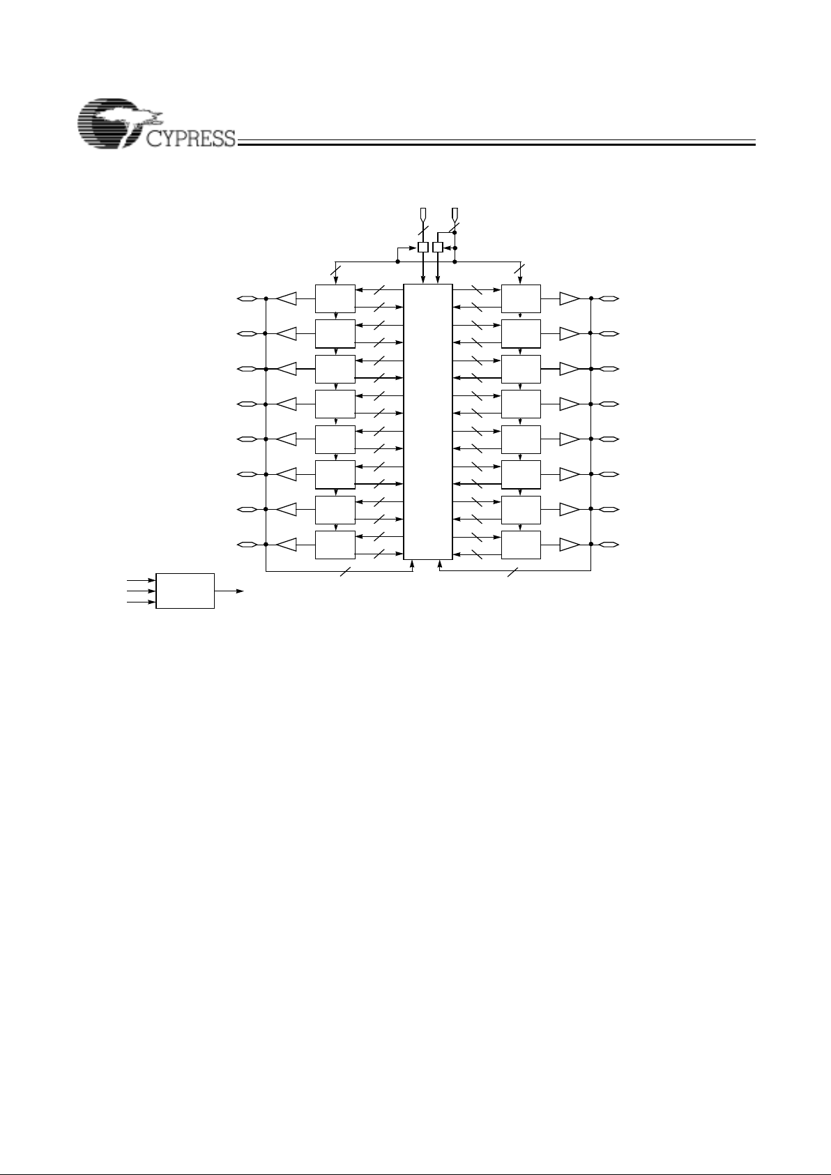
Architecture Overview of Ultra37000 Family
Programmable Interconnect Matrix
The Programmable Interconnect Matrix (PIM) consists of a
completely global routing matrix for signals from I/O pins and
feedbacks from the logic blocks. The PIM provides extremely
robust interconnection to avoid fitting and density limitations.
The inputs to the PIM consist of all I/O and dedicated input pins
and all mac r oc el l fe ed ba c ks fr om w i thi n t h e lo g ic b lo ck s. Th e
number of PIM input s increases with pin co unt and the number
of logic blocks. The outputs from the PIM are signals ro uted to
the appropriate logic blocks. Each logic block receives 36
inputs from the PIM and their compl ements, allow ing for 32-bit
operations to be implemented in a single pass through the
device. The wide number of inputs to the logic block also
improves the routing capacity of the Ultra37000 family.
An important feature of the PIM is its simple timing. The propagation delay through the PIM is accounted for in the timing
specifications fo r each devi ce. Th ere is no ad dition al del ay for
traveling through the PIM. In fact, all inputs travel through the
PIM. As a result, there are no route-dependent timing parameters on the Ultra37000 devices. The worst-case PIM delays
are incorporated in all appropriate Ultra37000 specifications.
Routing signals through the PIM is completely invisible to the
user . All routing is accomplished by software—no hand routing
is necessary. Warp™ and third- party dev elopm ent packag es
automatically route designs for the Ultra37000 family in a
matter of minutes. Finally, the rich routing resources of the
Ultra37000 family accommodate last minute logic changes
while maintaining fixed pin assignments.
Logic Block
The logic block is the basic building block of the Ultra37000
architect ure. It consis ts of a prod uct te rm arra y, an intelligen t
product-term allocator, 16 macrocells, and a number of I/O
cells. The number of I/O cells varies depending on the device
used. Refe r to Figure 1 for the block diagram.
Product Term Array
Each logic block features a 72 x 87 programmable product
term array. This array accepts 36 inputs from the PIM, which
originate from macrocell feedbacks and device pins. Active
LOW and active HIGH versions of each of these inputs are
generated to create the full 72-input field. The 87 product
terms in the array can be created from any of the 72 inputs.
Of the 87 product terms, 80 are for general-purpose use for
the 16 macrocells in the logic block. Four of the remaining
seven product terms i n the logic block are ou tpu t en abl e (O E)
product terms. Each of the OE product terms controls up to
eight of the 16 macrocells and is selectable on an individual
macrocell basis. In other words, each I/O cell can select
between one of two OE product terms to control the output
buffer. The first two of these four OE product terms are
available to the upper half of the I/ O macrocells in a logic block.
The other two OE product te rms are a vailabl e to the lower half
of the I/O macrocells in a logic block.
The next two product terms in each logic block are dedicated
asynchronous set and asynchronous reset product terms. The
final product te rm is th e produ ct term clo ck. The set, r eset, OE
and product term clock have polarity control to realize OR
functions in a single pass through the array.
Speed Bins
Device 200 167 154 143 125 100 83 66
CY37032V X X
CY37064V X X
CY37128V
XX X
CY37192V XX
CY37256V XXX
CY37384V XX
CY37512V
XXX
Shaded areas indicate preliminary speed bins.
Device-Package Offering & I/O Count
Device
44-
Lead
TQFP
44-
Lead
PLCC
44-
Lead
CLCC
48-
Lead
FBGA
84-
Lead
PLCC
84-
Lead
CLCC
100-
Lead
TQFP
100-
Lead
FBGA
160-
Lead
TQFP
160-
Lead
CQFP
208-
Lead
PQFP
208-
Lead
CQFP
256-
Lead
BGA
256-
Lead
FBGA
352-
Lead
BGA
400-
Lead
FBGA
CY37032V 37 37 37
CY37064V 37 37 37 37 69 69 69
CY37128V 69 69 69 85 133
CY37192V 125
CY37256V 133 133 165 197 197
CY37384V 165 197
CY37512V 165 165 197 269 269
Ultra37000 CPLD Fami
ly
Document #: 38-03007 Rev. *B Page 4 of 63
Low-Power Option
Each logic block can operate in high-speed mode for critical
path performance, or in low-power mode for power conservation. The logic bloc k mode is se t by the user on a l ogic block
by logic block basis.
Product Term Allocator
Through the product term allocator, software automatically
distributes product terms among the 16 macrocells in the logic
block as needed. A total of 80 p roduct terms are available from
the local product term array. The product term allocator
provides two important capabilities without affecting performance: product term steering and product term sharing.
Product Term Steering
Product term steering is the process of assigning product
terms to macrocell s as neede d. For e xamp le, if o ne ma croce ll
requires ten produc t terms whi le anot her need s just th ree, the
product term allocator will “steer” ten product terms to one
macrocell and three to the other. On Ultra37000 devices,
product terms are steere d on an ind ividu al bas is. Any n umber
between 0 and 16 product terms can be steered to any
macrocell. Note that 0 product terms is useful in cases where
a particular macrocell is unused or used as an input register.
Product Term Sharing
Product term sharing i s the process of using the same p roduct
term among multiple macrocells. For example, if more than
one output has one or more product terms in its equation that
are common to other outputs, those product terms are only
programmed once. The Ultra37000 product term allocator
allows sharing across groups of four output macrocells in a
variable fashion. The software automatically takes advantage
of this capability—the user does not have to intervene.
Note that neither product term sharing nor product term
steering have any effect on the speed of the product. All worstcase steering and sharing configurations have been incorporated in the timing specifications for the Ultra37000 devices.
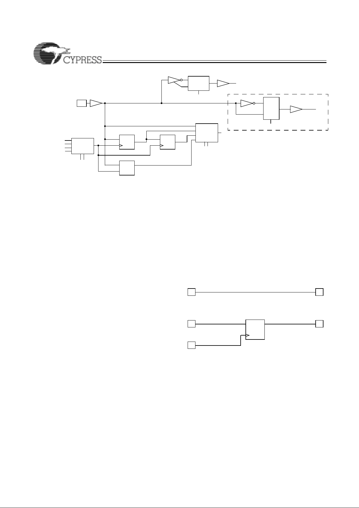
Ultra37000 Macrocell
Within each logic block there are 16 macrocells. Macrocells
can either be I/O Macrocells, which include an I/O Cell which
is associated with an I/O pin, or buried Macrocells, which do
not connect to an I/O. The combination of I/O Macrocells and
buried Macrocells varies from device to device.
Buried Macrocell
Figure 2 displays the architecture of buried macrocells. The
buried macrocell features a register tha t can be confi gured as
combinatorial, a D flip-flop, a T flip-flop, or a level-triggered
latch.
The register can be asynchronously set or asynchronously
reset at the logic block level with the separate set and reset
product terms. Each of these pro duct terms features programmable polarity. This allows the registers to be set or reset
based on an AND expression or an OR expression.
Clocking of the register is very flexible. Four global
synchronous clocks and a product term clock are available to
clock the register. Furthermore, each clock features programmable polarity so that registers can be triggered on falling as
well as rising edges (see the Clo cking sec tio n). Cloc k pol ari t y
is chosen at the logic block level.
The buried macrocell also supports input register capability.
The buried macrocell can be configured to act as an input
Figure 1. Logic Block with 50% Buried Macrocells
I/O
CELL
0
PRODUCT
TERM
ALLOCATOR
I/O
CELL
14
MACRO-
CELL
0
MACRO-
CELL
1
MACRO-
CELL
14
0−16
PRODUCT
TERMS
72 x 87
PRODUCT TERM
ARRAY
8036
8
16
TO
PIM
FROM
PIM
7
3
2
MACRO-
CELL
15
2
to cells
2, 4, 6 8, 10, 12
0−16
PRODUCT
TERMS
0−16
PRODUCT
TERMS
0−16
PRODUCT
TERMS

Ultra37000 CPLD Fami
ly
Document #: 38-03007 Rev. *B Page 5 of 63
register (D-type or latch) whose input comes from the I/O pin
associated with the neighboring macrocell. The output of all
buried macrocells is sent directly to the PIM regardless of its
configuration.
I/O Macrocell
Figure 2 illustrates the architecture of the I/O macrocell. The
I/O macrocell supports the same functions as the buried
macrocell with the addi tion of I/O capabi lity . At the output of the
macrocell, a polarity control mux is available to select active
LOW or active HIGH signals. This has the added advantage
of allowing significant logic reduction to occur in many applications.
The Ultra37000 m acrocell featu res a feedba ck path to the PIM
separate from the I/O pin input path. This means that if the
macrocell is buried (fed back internally only), the associated
I/O pin can still be used as an input.
Bus Hold Capabilities on all I/Os
Bus-hold, which is an i mprov ed ver sion o f the p opula r intern al
pull-up resistor, is a weak latch connected to the pin that does
not degrade the device’s performance. As a latch, bus-hold
maintains the last state of a pin when the pin is placed in a
high-impedance state, thus reducing system noise in businterface applications. Bus-hold additionally allows unused
device pins to remain unconnected on the board, which is
particularly useful during prototyping as designers can route
new signals to the device without cutting trace connections to
V
CC
or GND. For more informati on, see th e applicati on note
“Understanding Bus-Hold - A Feature of Cypress CPLDs.”
Programmable Slew Rate Control
Each output has a pro grammable c onfiguratio n bit, which sets
the output slew rate t o fast or slow . For design s concerned with
meeting FCC emissi ons st and ards the slo w edge pro vides for
lower system noise. For designs requiring very high performance the fast edge rate provides maximum system performance.
Ultra37000 CPLD Fami
ly
Document #: 38-03007 Rev. *B Page 6 of 63
f
Figure 2. I/O and Buried Macrocells
Figure 3. Input Macrocell
C2 C3
DECODE
C2 C3
DECODE
0
1
2
3
O
C6
C5
“0”
“1”
0
1
O
D/T/L
Q
R
P
0
1
2
3
O
C0
0
1
O
C4
FEEDBACK TO PIM
FEEDBACK TO PIM
BLOCK RESET
0−16
TERMS
I/O MACROCELL
I/O CELL
FROM PTM
0
1
O
D/T/L Q
R
P
FROM PTM
1
O
C7
FEEDBACK TO PIM
BURIED MACROCELL
0
ASYNCHRONOUS
PRODUCT
0−16
TERMS
PRODUCT
C1
4
0
1
2
3
Q
4
C24
C0C1
C24
C25
C25
4 SYNCHRONOUS CLOCKS (CLK0,CLK1,CLK2,CLK3)
1 ASYNCHRONOUS CLOCK(PTCLK)
BLOCK PRESET
ASYNCHRONOUS
FAST
SLOW
C26
SLEW
0
1
0
1
0
1
0
1
OE0
OE1
0
1
2
3
O
C12 C13
TO PIM
D
Q
D
Q
D
Q
LE
INPUT PIN
0
1
2
O
C10
FROM CLOCK
POLARITY MUXES
3
C11
Ultra37000 CPLD Fami
ly
Document #: 38-03007 Rev. *B Page 7 of 63
Clocking
Each I/O and buried macroc ell has access to four synchronou s
clocks (CLK0, CLK1, CLK2 and CLK3) as well as an
asynchronous product term clock PTCLK. Each input
macrocell has access to all four synchronous clocks.
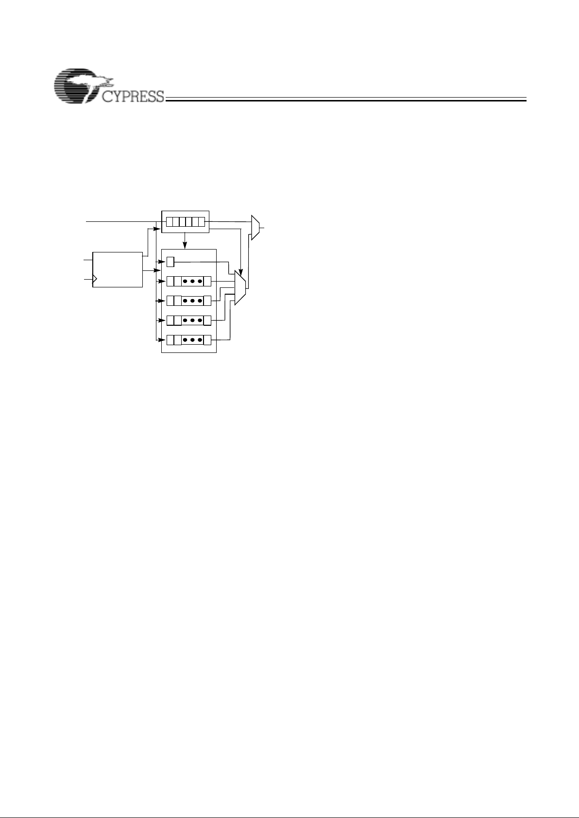
Dedicated Inputs/Clocks
Five pins on each member of the Ultra37000 family ar e designated as input-only. There are two types of dedicated inputs
on Ultra37000 devices: input pins and input/clock pins.
Figure 3 illustrates the architecture for input pins. Four input
options are available for the user: combinatorial, registered,
double-registered, or latched. If a registered or latched option
is selected, any one of the input clocks can be selected for
control.
Figure 4 illustrates the architecture for the input/clock pins.
Like the input pins, input/clock pins can be combinatorial,
registered, double-registered, or latched. In addition, these
pins feed the clocking structures throughout the device. The
clock path at the input has user-configurable polarity.
Product Term Clocking
In addition to the four synchronous clocks, the Ultra37000
family also has a product term clock for asynchronous
clocking. Each logic block has an independent product term
clock which is available to a ll 16 macrocells . Each product te rm
clock also supports user configurable polarity selection.
Timing Model
One of the most impo rtan t feature s of the U ltra3 7000 fa mily is
the simplicity of its timing. All delays are worst case and
system performance is unaf fected by the features use d. Figure
5 illustrates the true timing model for the 167-MHz devices in
high speed mode. For combinatorial paths, any input to any
output incurs a 6.5-ns worst-case delay regardless of the
amount of logic used. For synch ronous syst ems, the inp ut setup time to the outpu t macroc ells for a ny input is 3.5 ns a nd the
clock to output time is also 4.0 ns. These measurements are
for any output and synchronous clock, regardless of the logic
used.
The Ultra37000 features:
• No fanout delays
• No expander delays
• No dedicated vs. I/O pin delays
• No additional delay through PIM
• No penalty for using 0–16 product terms
• No added delay for steering product terms
• No added delay for sharing product terms
• No routing delays
• No output bypass delays
The simple timing model of the Ultra37000 family eliminates
unexpected performance penalties.
JTAG and PCI Standards
PCI Compliance
5V operation of the Ultra37000 is fully compliant with the PCI
Local Bus Specification published by the PCI Special Interest
Group. The 3.3V products meet all PCI requirements except
for the output 3.3V clamp, which is in direct conflict with 5V
tolerance. The Ultra37000 family’s simple and predictable
timing model ensures compliance with the PCI AC specifications independent of the design.
Figure 4. Input/Clock Macrocell
0
1
2
3
O
C10C11
TO PIM
D
Q
D
Q
D
Q
LE
INPUT/CLOCK PIN
0
1
2
O
FROM CLOCK
CLOCK PINS
0
1
O
C12
TO CLOCK MUX ON
ALL INPUT MACROCELLS
TO CLOCK MUX
IN EACH
3
0
1
CLOCK POLARITY MUX
ONE PER LOGIC BLOCK
FOR EACH CLOCK INPUT
POLARITY INPUT
LOGIC BLOCK
C8
C9
C13, C14, C15 OR C16
O
Figure 5. Timing Model for CY37128
COMBINATORIAL SIGNAL
REGISTERED SIGNAL
D,T,L O
CLOCK
INPUT
INPUT
OUTPUT
OUTPUT
tS = 3.5 ns
t
CO
= 4.5 ns
t
PD
= 6.5 ns
Ultra37000 CPLD Fami
ly
Document #: 38-03007 Rev. *B Page 8 of 63
IEEE 1149.1-compliant JTAG
The Ultra37000 family has an IEEE 1149.1 JTAG interface for
both Boundary Scan and ISR.
Boundary Scan
The Ultra37000 family supports Bypass, Sample/Preload,
Extest, Idcode, and Usercode boundary sc an instructions. The
JTAG interface is shown in Figure 6.
In-System Reprogramming (ISR)
In-System Reprogram ming is the comb ination of the capability
to program or reprogram a device on-board, and the ability to
support design changes without changing the system timing
or device pinout. This combination means design changes
during debug or field upgrades do not cause board respins.
The Ultra37000 family implements ISR by providing a JTAG
compliant interface for on-board programming, robust routing
resources for pinout flexibility, and a simple timing model for
consistent system performance.
Development Software Support
Warp
Warp is a st ate-of-the-art compil er and complete CPLD de sign
tool. For design entry , Warp provides an IEEE-STD-1076/1164
VHDL text editor , an IEEE-STD-1364 V erilo g text editor, and a
graphical finite state machine editor. It provides optimized
synthesis and fitting by replacing basic circuits with ones preoptimized for the target device, by implementing logic in
unused memory an d by perfect comm unication betwee n fitting
and synthesis. To facilitate design and debugging, Warp
provides graphical timing simulation and analysis.
Warp Professional
™
Warp Professional contains several additional features. It
provides an extra method of design entry with its graphical
block diagram ed itor. It allows up to 5 ms timin g simulation
instead of only 2 ms. It allows comp arison of waveforms before
and after design changes.
Warp Enterprise
™
Warp Enterprise provides even more features. It provides
unlimited timing simulation and source-level behavioral
simulation as well as a debug ger. It has the ability to generate
graphical HDL blocks from HDL text. It can even generate
testbenches.
Warp is available for PC and UNIX platforms. Some features
are not avai lable i n the U NIX ve rsion. For fur ther infor matio n
see the Warp for PC, W arp for UNIX, Warp Profession al and
Warp Enterprise data sheets on Cypress’s web site
(www.cypress.com).
Third-Party Software
Although Warp is a complete CP LD developm ent tool o n its
own, it interfaces with nearly every third party EDA tool. All
major third-party software vendors provide support for the
Ultra37000 family o f de vi ce s. Refe r to the th ird-party software
data sheet or contact your local sales office for a list of
currently supported third-p a rty vendors.
Programming
There are four programming options available for Ultra37000
devices. The first method is to use a PC with the 37000
UltraISR programming cable and software. With this method,
the ISR pins of the Ultra37000 devices are routed to a
connector at the edge of the printed circuit board. The 37000
UltraISR programming cable is then connected between the
parallel port of the PC and this connector. A simple configuration file instructs the ISR software of the programming
operations to be perform ed on each of the Ultra 37000 device s
in the system. The ISR s oftware then automatic ally co mpletes
all of the necessary dat a manipulatio ns required to accomplis h
the programming, reading, verifying, and other ISR functions.
For more information on the Cypress ISR Interface, see the
ISR Programming Kit data sheet (CY3700i).
The second meth od for programming U ltra37000 device s is on
automatic test equip ment (A TE). This i s accomplished throu gh
a file created by the ISR sof tware. Check th e Cypress web site
for the latest ISR software download information.
The third programming option for Ultra37000 devices is to
utilize the embedded controller or processor that already
exists in the s ystem. T he Ultr a37000 ISR softw are assi sts in
this method by converting the device JEDEC maps into the
ISR serial stream that c ont ains the ISR ins tructi on inf ormati on
and the addresses and data of locations to be programmed.
The embedded controller then simply directs this ISR stream
to the chain of Ultra37000 devices to complete the desired
reconfiguring or diagnostic operations. Contact your local
sales office for information on availability of this option.
The fourth method for programming Ultra37000 devices is to
use the same programmer that is currently being used to
program F
LASH370i devices.
For all pinout, electrical, and timing requirements, refer to
device data shee ts. For ISR cable an d software speci fications,
refer to the UltraISR kit data sheet (CY3700i).
Third-Party Programmers
As with development software, Cypress support is available
on a wide va riety of thi rd-par ty prog rammer s. All majo r thir dparty programmers (including BP Micro, Data I/O, and SMS)
support the Ultra37000 family.
Figure 6. JTAG Interface
Instruction Register
Boundary Scan
idcode
Usercode
ISR Prog .
Bypass Reg.
Data Registers
JTAG
TAP
CONTROLLER
TDO
TDI
TMS
TCK
Ultra37000 CPLD Fami
ly
Document #: 38-03007 Rev. *B Page 9 of 63
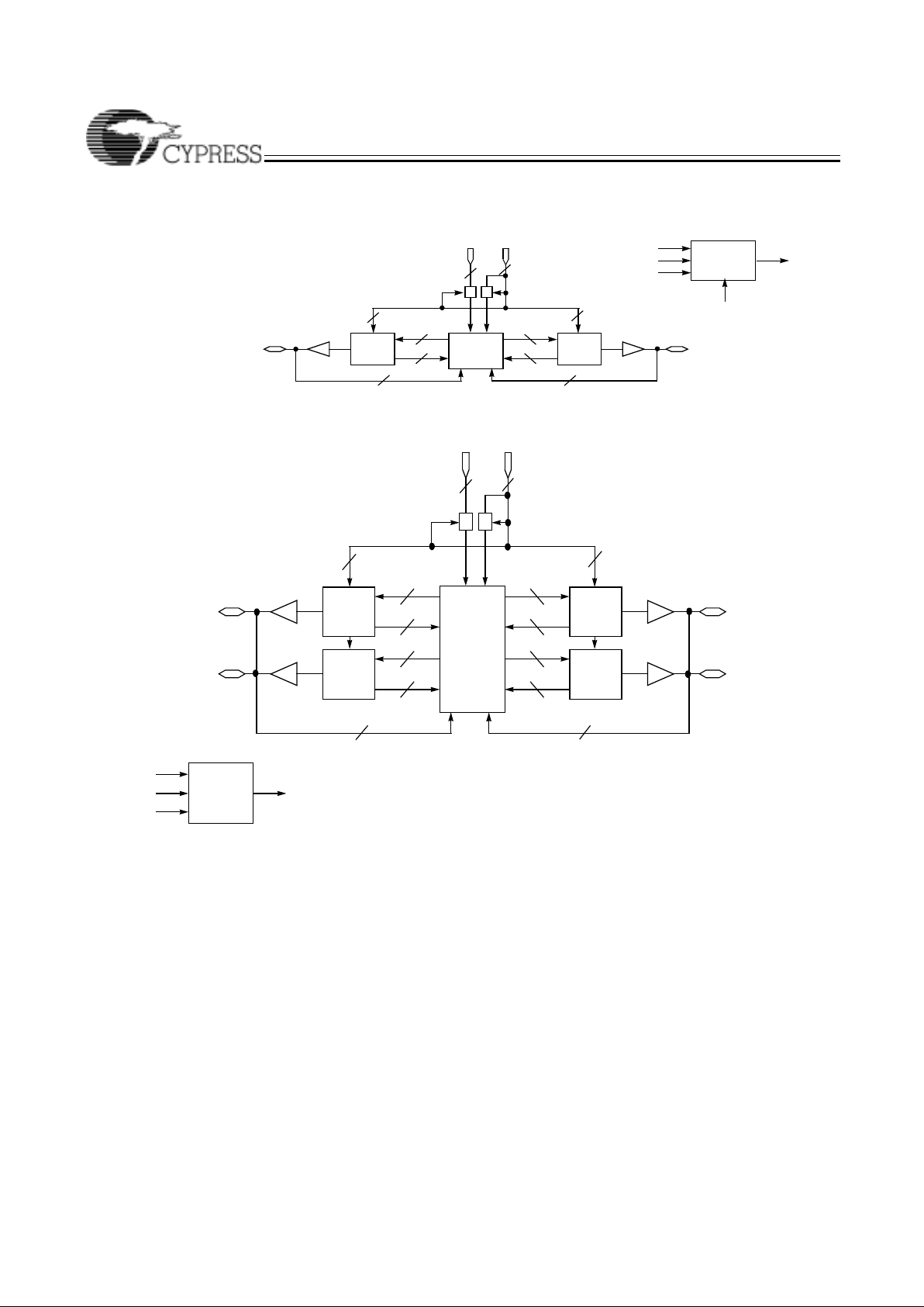
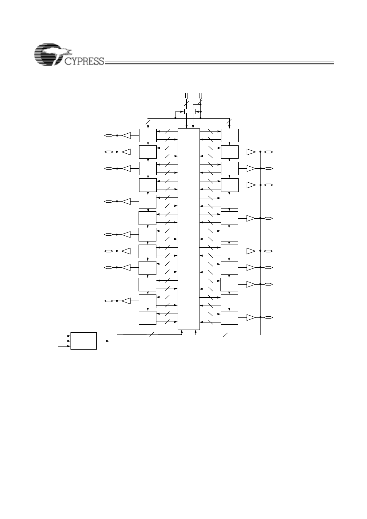
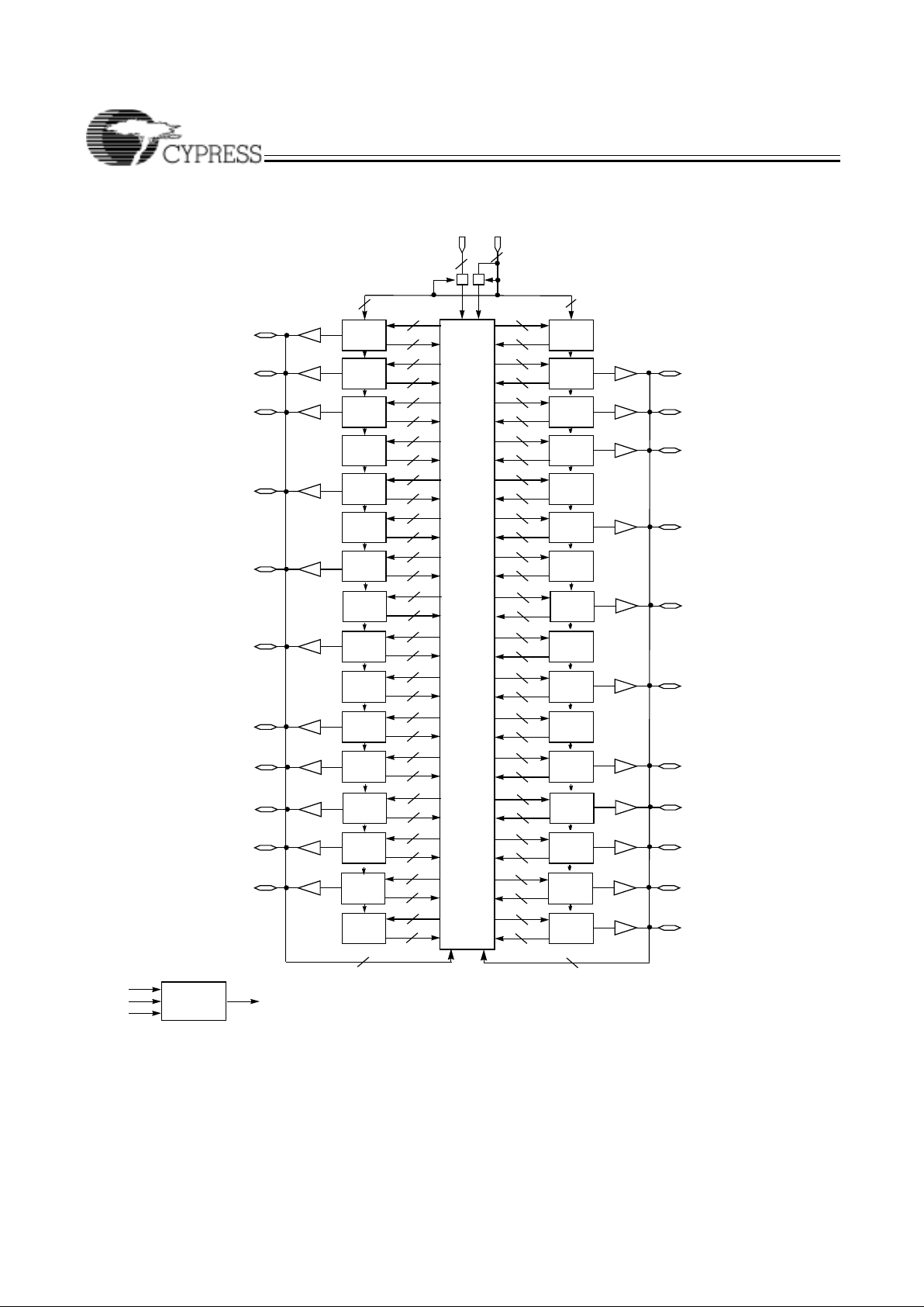
Logic Block Diagrams
CY37032/CY37032V
LOGIC
BLOCK
B
LOGIC
BLOCK
A
36
16
36
16
Input
Clock/
Input
16 I/Os
16 I/Os
I/O
0
−I/O
15
I/O16−I/O
31
4
4
4
16
16
TDI
TCK
TMS
TDO
JTAG Tap
Controller
1
PIM
JTAG
EN
LOGIC
BLOCK
D
LOGIC
BLOCK
C
LOGIC
BLOCK
A
LOGIC
BLOCK
B
36
16
36
16
36
16
36
16
Input
Clock/
Input
16 I/Os
16 I/Os
16 I/Os
16 I/Os
I/O
0
-I/O
15
I/O16-I/O
31
I/O48-I/O
63
I/O32-I/O
47
4
4
4
32
32
TDI
TCK
TMS
TDO
JTAG Tap
Controller
1
PIM
CY37064/CY37064V (100-Lead TQFP)
Ultra37000 CPLD Fami
ly
Document #: 38-03007 Rev. *B Page 10 of 63
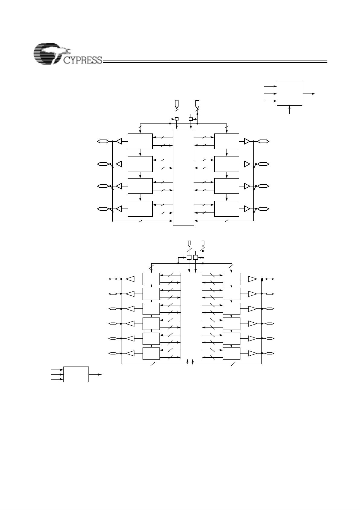
Logic Block Diagrams (continued)
TDI
TCK
TMS
TDO
JTAG Tap
Controller
CY37128/CY37128V (160-lead TQFP)
PIM
INPUT
MACROCELL
CLOCK
INPUTS
4 4
36
16
16
36
LOGIC
BLOCK
36
16
16
36
16 I/Os
36 36
36
16
16
36
16
16
64
64
41
INPUT/CLOCK
MACROCELLS
I/O
0
–I/O
15
A
INPUTS
LOGIC
BLOCK
C
LOGIC
BLOCK
B
LOGIC
BLOCK
D
LOGIC
BLOCK
H
LOGIC
BLOCK
G
LOGIC
BLOCK
F
LOGIC
BLOCK
E
I/O16–I/O
31
I/O32–I/O
47
I/O28–I/O
63
I/O
112
–I/O
127
I/O96–I/O
111
I/O80–I/O
95
I/O64–I/O
79
16 I/Os
16 I/Os
16 I/Os
16 I/Os
16 I/Os
16 I/Os
16 I/Os
JTAG
EN
LOGIC
BLOCK
H
LOGIC
BLOCK
L
LOGIC
BLOCK
I
LOGIC
BLOCK
J
LOGIC
BLOCK
K
LOGIC
BLOCK
A
LOGIC
BLOCK
B
LOGIC
BLOCK
C
LOGIC
BLOCK
D
LOGIC
BLOCK
E
LOGIC
BLOCK
G
LOGIC
BLOCK
F
36
16
36
16
36
16
36
16
36
16
36
16
36
16
36
16
36
16
36
16
36
16
36
16
PIM
Input
Clock/
Input
10 I/Os
10 I/Os
10 I/Os
10 I/Os
10 I/Os
10 I/Os
10 I/Os
10 I/Os
10 I/Os
10 I/Os
10 I/Os
10 I/Os
I/O
0
–I/O
9
I/O10–I/O
19
I/O20–I/O
29
I/O30–I/O
39
I/O40–I/O
49
I/O50–I/O
59
I/O
110
–I/O
119
I/O
100
–I/O
109
I/O90–I/O
99
I/O80–I/O
89
I/O70–I/O
79
I/O60–I/O
69
4
4
4
6060
TDI
TCK
TMS
TDO
JTAG Tap
Controller
1
CY37192/CY37192V (160-lead TQFP)
Ultra37000 CPLD Fami
ly
Document #: 38-03007 Rev. *B Page 11 of 63
Logic Block Diagrams (continued)
CY37256/CY37256V (256-lead BGA)
LOGIC
BLOCK
G
LOGIC
BLOCK
H
LOGIC
BLOCK
I
LOGIC
BLOCK
J
LOGIC
BLOCK
L
LOGIC
BLOCK
P
LOGIC
BLOCK
M
LOGIC
BLOCK
N
LOGIC
BLOCK
O
LOGIC
BLOCK
A
LOGIC
BLOCK
B
LOGIC
BLOCK
C
LOGIC
BLOCK
D
LOGIC
BLOCK
E
LOGIC
BLOCK
K
LOGIC
BLOCK
F
36
16
36
16
36
16
36
16
36
16
36
16
36
16
36
16
36
16
36
16
36
16
36
16
36
16
36
16
36
16
36
16
PIM
Input
Clock/
Input
12 I/Os
12 I/Os
12 I/Os
12 I/Os
12 I/Os
12 I/Os
12 I/Os
12 I/Os
12 I/Os
12 I/Os
12 I/Os
12 I/Os
12 I/Os
12 I/Os
12 I/Os
12 I/Os
I/O
0
−I/O
11
I/O12−I/O
23
I/O24−I/O
35
I/O36−I/O
47
I/O48−I/O
59
I/O60−I/O
71
I/O72−I/O
83
I/O84−I/O
95
I/O
180
−I/O
191
I/O
168
−I/O
179
I/O
156
−I/O
167
I/O
144
−I/O
155
I/O
132
−I/O
143
I/O
120
−I/O
131
I/O
108
−I/O
119
I/O96−I/O
107
4
4
4
96
96
TDI
TCK
TMS
TDO
JTAG Tap
Controller
1
Ultra37000 CPLD Fami
ly
Document #: 38-03007 Rev. *B Page 12 of 63
Logic Block Diagrams (continued)
CY37384/CY37384V (256-Lead BGA)
LOGIC
BLOCK
AH
LOGIC
BLOCK
AI
LOGIC
BLOCK
BD
LOGIC
BLOCK
BE
LOGIC
BLOCK
BG
LOGIC
BLOCK
BL
LOGIC
BLOCK
BI
LOGIC
BLOCK
BJ
LOGIC
BLOCK
BK
LOGIC
BLOCK
AA
LOGIC
BLOCK
AB
LOGIC
BLOCK
AC
LOGIC
BLOCK
AD
LOGIC
BLOCK
AF
LOGIC
BLOCK
BF
LOGIC
BLOCK
AG
36
16
36
16
36
16
36
16
36
16
36
16
36
16
36
16
36
16
36
16
36
16
36
16
36
16
36
16
36
16
36
16
PIM
Input
Clock/
Input
12 I/Os
12 I/Os
12 I/Os
12 I/Os
12 I/Os
12 I/Os
12 I/Os
12 I/Os
12 I/Os
12 I/Os
12 I/Os
I/O
0
−I/O
11
I/O12−I/O
23
I/O24−I/O
35
I/O48−I/O
59
I/O60−I/O
71
I/O72−I/O
83
I/O
168
−I/O
191
I/O
156
−I/O
179
I/O
144
−I/O
167
I/O
120
−I/O
143
I/O
108
−I/O
131
4
4
4
96
96
TDI
TCK
TMS
TDO
JTAG Tap
Controller
1
LOGIC
BLOCK
AJ
LOGIC
BLOCK
BC
16
16
12 I/Os
I/O
96
−I/O
119
LOGIC
BLOCK
AK
LOGIC
BLOCK
BB
16
16
12 I/Os
I/O
84
−I/O
95
LOGIC
BLOCK
AL
LOGIC
BLOCK
BA
16
16
12 I/Os
I/O
96
−I/O
107
LOGIC
BLOCK
AE
LOGIC
BLOCK
BH
16
16
12 I/Os
12 I/Os
I/O
36
−I/O
47
I/O
132
−I/O
155
36
36
36
36
36
36
36
36
Ultra37000 CPLD Fami
ly
Document #: 38-03007 Rev. *B Page 13 of 63
Logic Block Diagrams (continued)
CY37512/CY37512V (352-Lead BGA)
LOGIC
BLOCK
AG
LOGIC
BLOCK
AH
LOGIC
BLOCK
BI
LOGIC
BLOCK
BJ
LOGIC
BLOCK
BL
LOGIC
BLOCK
BP
LOGIC
BLOCK
BM
LOGIC
BLOCK
BN
LOGIC
BLOCK
BO
LOGIC
BLOCK
AA
LOGIC
BLOCK
AB
LOGIC
BLOCK
AC
LOGIC
BLOCK
AD
LOGIC
BLOCK
AE
LOGIC
BLOCK
BK
LOGIC
BLOCK
AF
36
16
36
16
36
16
36
16
36
16
36
16
36
16
36
36
36
16
36
16
36
16
36
16
36
16
36
16
36
16
Input
Clock/
Input
12 I/Os
12 I/Os
12 I/Os
12 I/Os
12 I/Os
12 I/Os
12 I/Os
12 I/Os
12 I/Os
12 I/Os
12 I/Os
12 I/Os
12 I/Os
I/O
0
−
I/O
11
I/O12−
I/O
23
I/O24−
I/O
35
I/O36−
I/O
47
I/O48−
I/O
59
I/O60−
I/O
71
I/O72−
I/O
83
I/O84−
I/O
95
I/O
252
−
I/O
263
I/O
240
−
I/O
251
I/O
228
−
I/O
239
I/O
216
−
I/O
227
I/O
204
−
I/O
215
4
4
4
TDI
TCK
TMS
TDO
JTAG Tap
Controller
1
PIM
16
36
36
16
LOGIC
BLOCK
AI
LOGIC
BLOCK
BH
12 I/Os
I/O
96
−
I/O
107
16
36
36
16
LOGIC
BLOCK
AJ
LOGIC
BLOCK
BG
12 I/Os
12 I/Os
I/O
108
−
I/O
119
I/O
192
−
I/O
203
16
36
36
16
LOGIC
BLOCK
AK
LOGIC
BLOCK
BF
12 I/Os
I/O
120
−
I/O
131
16
36
36
16
LOGIC
BLOCK
AL
LOGIC
BLOCK
BE
12 I/Os
I/O
180
−
I/O
191
16
36
36
16
LOGIC
BLOCK
AM
LOGIC
BLOCK
BD
12 I/Os
I/O
168
−
I/O
179
16
36
36
16
LOGIC
BLOCK
AN
LOGIC
BLOCK
BC
12 I/Os
I/O
156
−
I/O
167
16
36
36
16
LOGIC
BLOCK
AO
LOGIC
BLOCK
BB
12 I/Os
I/O
144
−
I/O
155
16
36
36
16
LOGIC
BLOCK
AP
LOGIC
BLOCK
BA
12 I/Os
I/O
132
−
I/O
143
16
132132
16
Ultra37000 CPLD Fami
ly
Document #: 38-03007 Rev. *B Page 14 of 63
5.0V Device Characteristics
Maximum Ratings
(Above which the us efu l l ife ma y be impaired. For us er gui delines, not tested.)
Storage Temperature .................................–65°C to +150°C
Ambient Temperature with
Power Applied.............................................–55°C to +125°C
Supply Voltage to Ground Potential...............–0.5V to +7.0V
DC Voltage Applied to Outputs
in High-Z State................................................–0.5V to +7.0V
DC Input Voltage............................................–0.5V to +7.0V
DC Program Voltage.............................................4.5 to 5.5V
Current into Outputs....................................................16 mA
Static Discharge Voltage...........................................> 2001V
(per MIL-STD-883, Method 3015)
Latch-up Current.....................................................> 200 mA
Operating Range
[2]
Range
Ambient
Temperature
[2]
Junction
Temperature
Output
Condition V
CC
V
CCO
Commercial 0°C to +70°C 0°C to +90°C 5V 5V ± 0.25V 5V ± 0.25V
3.3V 5V ± 0.25V 3.3V ± 0.3V
Industrial –40°C to +85°C –40°C to +105°C 5V 5V ± 0.5V 5V ± 0.5V
3.3V 5V ± 0.5V 3.3V ± 0.3V
Military
[3]
–55°C to +125°C –55°C to +130°C 5V 5V ± 0.5V 5V ± 0.5V
3.3V 5V ± 0.5V 3.3V ± 0.3V
5.0V Device Electrical Characteristics Over the Operating Range
Parameter Description T est Conditi ons Min. Typ. Max. Unit
V
OH
Output HIGH Voltage VCC = Min. IOH = –3.2 mA (Com’l/Ind)
[4]
2.4 V
IOH = –2.0 mA (Mil)
[4]
2.4 V
V
OHZ
Output HIGH Voltage with
Output Disabled
[5]
VCC = Max. IOH = 0 µA (Com’l)
[6]
4.2 V
IOH = 0 µA (Ind/Mil)
[6]
4.5 V
IOH = –100 µA (Com’l)
[6]
3.6 V
IOH = –150 µA (Ind/Mil)
[6]
3.6 V
V
OL
Output LOW Voltage VCC = Min. IOL = 16 mA (Com’l/Ind)
[4]
0.5 V
IOL = 12 mA (Mil)
[4]
0.5 V
V
IH
Input HIGH Voltage Guaranteed Input Logical HIGH Voltage for all Inputs
[7]
2.0 V
CCmax
V
V
IL
Input LOW Voltage Guaranteed Input Logical LOW Voltage for all Inputs
[7]
–0.5 0.8 V
I
IX
Input Load Current VI = GND OR VCC, Bus-Hold Disabled –10 10 µA
I
OZ
Output Leakage Current VO = GND or VCC, Output Disabled, Bus-Hold Disabled –50 50 µA
I
OS
Output Short Circuit Current
[8, 5]
VCC = Max., V
OUT
= 0.5V –30 –160 mA
I
BHL
Input Bus-Hold LOW
Sustaining Current
VCC = Min., VIL = 0.8V +75 µA
I
BHH
Input Bus-Hold HIGH
Sustaining Current
VCC = Min., VIH = 2.0V –75 µA
I
BHLO
Input Bus-Hold LOW
Overdrive Current
VCC = Max. +500 µA
I
BHHO
Input Bus-Hold HIGH
Overdrive Current
VCC = Max. –500 µA
Notes:
2. Normal Programming Conditions apply across Ambient Temperature Range for specified programming methods. For more information on programming the
Ultra37000 Family devices, please refer to the Application Note titled “An Introduction to In System Reprogramming with the Ultra37000.”
3. T
A
is the “Instant On” case temperature.
4. IOH = –2 mA, IOL = 2 mA for TDO.
5. Tested initially and after any design or process changes that may affect these parameters.
6. When the I/O is output disabled, the bus-hold circuit can weakly pull the I/O to above 3.6V if no leakage current is allowed. Note that all I/Os are output disabled
during ISR programming. Refer to the application note “Understanding Bus-Hold” for additional information.
7. These are absolute values with respect to device ground. All overshoots due to system or tester noise are included.
8. Not more than one output should be tested at a time. Duration of the short circuit should not exceed 1 second. V
OUT
= 0.5V has been chosen to avoid test
problems caused by tester ground degradation.
Ultra37000 CPLD Fami
ly
Document #: 38-03007 Rev. *B Page 15 of 63
3.3V Device Characteristics
Maximum Ratings
(Above which the us efu l l ife ma y be impaired. For us er gui delines, not tested.)
Storage Temperature .................................–65°C to +150°C
Ambient Temperature with
Power Applied.............................................–55°C to +125°C
Supply Voltage to Ground Potential...............–0.5V to +4.6V
DC Voltage Applied to Outputs
in High-Z State................................................–0.5V to +7.0V
DC Input Voltage............................................–0.5V to +7.0V
DC Program Voltage.............................................3.0 to 3.6V
Current into Outputs......................................................8 mA
Static Discharge Voltage............................................>2001V
(per MIL-STD-883, Method 3015)
Latch-up Current......................................................>200 mA
Inductance
[5]
Parameter Description
Test
Conditions
44-
Lead
TQFP
44-
Lead
PLCC
44-
Lead
CLCC
84-
Lead
PLCC
84-
Lead
CLCC
100-
Lead
TQFP
160-
Lead
TQFP
208-
Lead
PQFP Unit
L Maximum Pin
Inductance
VIN = 5.0V
at f = 1 MHz
2 5 2 8 5 8 9 11 nH
Capacitance
[5]
Parameter Description Test Conditions Max. Unit
C
I/O
Input/Output Capacitance VIN = 5.0V at f = 1 MHz at TA = 25°C 10 pF
C
CLK
Clock Signal Capacitance VIN = 5.0V at f = 1 MHz at TA = 25°C 12 pF
C
DP
Dual Function Pins
[9]
VIN = 5.0V at f = 1 MHz at TA = 25°C 16 pF
Endurance Characteristics
[5]
Parameter Description T est Condit ions Min. Typ. Unit
N Minimum Reprogramming Cycles Normal Programming Conditions
[2]
1,000 10,000 Cycles
Operating Range
[2]
Range Ambient Temperature
[2]
Junction Te mperature V
CC
[10]
Commercial 0°C to +70°C 0°C to +90°C 3.3V ± 0.3V
Industrial –40°C to +85°C –40°C to +105°C
3.3V ± 0.3V
Military
[3]
–55°C to +125°C –55°C to +130°C 3.3V ± 0.3V
3.3V Device Electrical Characteristics Over the Operating Range
Parameter Description Test Conditions Min. Max. Unit
V
OH
Output HIGH Voltage VCC = Min. IOH = –4 mA (Com’l)
[4]
2.4 V
IOH = –3 mA (Mil)
[4]
V
OL
Output LOW Voltage VCC = Min. IOL = 8 mA (Com’l)
[4]
0.5 V
IOL = 6 mA (Mil)
[4]
V
IH
Input HIGH Voltage Guaranteed In put Logical HIGH V oltage for
all Inputs
[7]
2.0 5.5 V
V
IL
Input LOW Voltage Guaranteed Inpu t Lo gic al LO W Voltage for
all Inputs
[7]
–0.5 0.8 V
I
IX
Input Load Current VI = GND OR VCC, Bus-Hold Disabled –10 10 µA
I
OZ
Output Leakage Current VO = GND or VCC, Output Disabled, Bus-
Hold Disabled
–50 50 µA
I
OS
Output Short Circuit Current
[8, 5]
VCC = Max., V
OUT
= 0.5V –30 –160 mA
I
BHL
Input Bus-Hold LOW Sustaining
Current
VCC = Min., VIL = 0.8V +75 µA
Notes:
9. Dual pins are I/O with JTAG pins.
10. For CY37064VP100-143AC, CY37064VP100-143BBC, CY37064VP44-143AC, CY37064VP48-143BAC; Operating Range: V
CC
is 3.3V± 0.16V.
Ultra37000 CPLD Fami
ly
Document #: 38-03007 Rev. *B Page 16 of 63
I
BHH
Input Bus-Hold HIGH Sustaining
Current
VCC = Min., VIH = 2.0V –75 µA
I
BHLO
Input Bus-Hold LOW Overdrive
Current
VCC = Max. +500 µA
I
BHHO
Input Bus-Hold HIGH Overdrive
Current
VCC = Max. –500 µA
Inductance
[5]
Parameter Description
Test
Conditions
44-
Lead
TQFP
44-
Lead
PLCC
44-
Lead
CLCC
84-
Lead
PLCC
84-
Lead
CLCC
100-
Lead
TQFP
160-
Lead
TQFP
208-
Lead
PQFP Unit
L Maximum Pin
Inductance
VIN = 3.3V
at f = 1 MHz
2 5 2 8 5 8 9 11 nH
Capacitance
[5]
Parameter Description Test Conditions Max. Unit
C
I/O
Input/Output Capacitance VIN = 3.3V at f = 1 MHz at TA = 25°C 8 pF
C
CLK
Clock Signal Capacitance VIN = 3.3V at f = 1 MHz at TA = 25°C 12 pF
C
DP
Dual Functional Pins
[9]
VIN = 3.3V at f = 1 MHz at TA = 25°C 16 pF
Endurance Characteristics
[5]
Parameter Description T est Condit ions Min. Typ. Unit
N Minimum Reprogramming Cycles Normal Programming Conditions
[2]
1,000 10,000 Cycles
3.3V Device Electrical Characteristics Over the Operating Range (continued)
Parameter Description Test Conditions Min. Max. Unit
AC Characteristics
5.0V AC Test Loads and Waveforms
90%
10%
3.0V
GND
90%
10%
ALL INPUT PULSES
5V
OUTPUT
35 pF
INCLUDING
JIG AND
SCOPE
5V
OUTPUT
5 pF
INCLUDING
JIG AND
SCOPE
(a) (b)
<2 ns
OUTPUT
238Ω (COM’L)
319Ω(MIL)
170Ω (COM’L)
236Ω(MIL)
99Ω (COM’L)
136Ω (MIL)
Equivalent to: THÉVENIN EQUIVALENT
2.08V (COM'L)
2.13V (MIL)
238Ω (COM'L)
319Ω(MIL)
170Ω (COM'L)
236Ω(MIL)
<2 ns
(c)
5 OR 35 pF
Ultra37000 CPLD Fami
ly
Document #: 38-03007 Rev. *B Page 17 of 63
3.3V AC Test Loads and Waveforms
AC Characteristics
90%
10%
3.0V
GND
90%
10%
ALL INPUT PULSES
3.3V
OUTPUT
35 pF
INCLUDING
JIG AND
SCOPE
3.3V
OUTPUT
5 pF
INCLUDING
JIG AND
SCOPE
(a) (b)
<2 ns
OUTPUT
295Ω (COM’L)
393Ω(MIL)
340Ω (COM’L)
453Ω(MIL)
Equivalent to: THÉVENIN EQUIVALENT
1.77V (COM'L)
1.77V (MIL)
295Ω (COM'L)
393Ω(MIL)
340Ω (COM'L)
453Ω(MIL)
<2 ns
(c)
270Ω (MIL)
158Ω(COM’L)
5 OR 35 pF
Parameter
[11]
V
X
Output Waveform—Measurement Level
t
ER(–)
1.5V
t
ER(+)
2.6V
t
EA(+)
1.5V
t
EA(–)
V
the
(d) Test Waveforms
V
OH
V
X
0.5V
V
OL
V
X
0.5V
V
X
V
O
H
0.5V
V
X
V
OL
0.5V
Switching Characteristics Over the Operating Range
[12]
Parameter Description Unit
Combinatorial Mode Parameters
t
PD
[13, 14, 15]
Input to Combinatorial Output ns
t
PDL
[13, 14, 15]
Input to Output Through Transparent Input or Output Latch ns
t
PDLL
[13, 14, 15]
Input to Output Through Transparent Input and Output Latches ns
t
EA
[13, 14, 15]
Input to Output Enable ns
t
ER
[11, 13 ]
Input to Output Disable ns
Input Register Parameters
t
WL
Clock or Latch Enable Input LOW Time
[8]
ns
Notes:
11. t
ER
measured with 5-pF AC Test Load and tEA measured with 35-pF AC Test Load.
12. All AC parameters are measured with two outputs switching and 35-pF AC Test Load.
13. Logic Blocks operating in Low-Power Mode, add t
LP
to this spec.
14. Outputs using Slow Output Slew Rate, add t
SLEW
to this spec.
15. When V
CCO
= 3.3V, add t
3.3IO
to this spec.
Ultra37000 CPLD Fami
ly
Document #: 38-03007 Rev. *B Page 18 of 63
t
WH
Clock or Latch Enable Input HIGH Time
[8]
ns
t
IS
Input Register or Latch Set-up Time ns
t
IH
Input Register or Latch Hold Time ns
t
ICO
[13, 14, 15]
Input Register Clock or Latch Enable to Combinatorial Output ns
t
ICOL
[13, 14, 15]
Input Register Clock or Latch Enable to Output Through Transparent Output Latch ns
Synchronous Clocking Parameters
t
CO
[14, 15]
Synchronous Clock (CLK0, CLK1, CLK2, or CLK3) or Latch Enable to Output ns
t
S
[13]
Set-Up Time from Input to Sync. Clk (CLK0, CLK1, CLK2, or CLK3) or Latch Enable ns
t
H
Register or Latch Data Ho ld Time ns
t
CO2
[13, 14, 15]
Output Synchronous Clock (CLK0, CLK1, CLK2, or CLK3) or Latch Enable to Com binatoria l Output
Delay (Through Logic Array)
ns
t
SCS
[13]
Output Synchronous Clock (CLK0, CLK1, CLK2, or CLK3) or Latch Enable to Outpu t Sy nc hro nou s
Clock (CLK
0
, CLK1, CLK2, or CLK3) or Latch Enable (Through Logic Array)
ns
t
SL
[13]
Set-Up Time from Inp ut T hrou gh Transparent Latch to Output Regist er Sy nc hron ou s C l ock (CL K0
CLK
1
, CLK2, or CLK3) or Latch Enable
ns
t
HL
Hold Time for Input Through Transparent Latch from Output Register Synchronous Clock (CLK0,
CLK
1
, CLK2, or CLK3) or Latch Enable
ns
Product Term Clock ing Param eters
t
COPT
[13, 14, 15]
Product Term Clock or Latch Enable (PTCLK) to Output ns
t
SPT
Set-Up Time from Input to Product Term Clock or Latch Enable (PTCLK) ns
t
HPT
Register or Latch Data Ho ld Time ns
t
ISPT
[13]
Set-Up Time for Buried Register used as an Input Register from Input to Product Term Clock or
Latch Enable (PTCLK)
ns
t
IHPT
Buried Reg ister Used as an Input Register or Lat ch Data Hold Time ns
t
CO2PT
[13, 14, 15]
Product Term Clock or Latch Enable (PTCLK) to Output Delay (Through Logic Array) ns
Pipelined Mode Parameters
t
ICS
[13]
Input Register Synchronous Clock (CLK0, CLK1, CLK2, or CLK3) to Output Register S ync hro nou s
Clock (CLK0, CLK1, CLK2, or CLK3)
ns
Operating Frequency Parameters
f
MAX1
Maximum Frequency with Internal Feedback (Lesser of 1/t
SCS
, 1/(tS + tH), or 1/tCO)
[5]
MHz
f
MAX2
Maximum Frequency Data Path in Output Registered/Latched Mode (Lesser of 1/(tWL + tWH),
1/(t
S+tH
), or 1/tCO)
[5]
MHz
f
MAX3
Maximum Frequency with External Feedback (Lesser of 1/(tCO + tS) or 1/(tWL + tWH)
[5]
MHz
f
MAX4
Maximum Frequency in Pipelined Mode (Lesser of 1/(tCO + tIS), 1/t
ICS
, 1/(tWL + tWH), 1/(tIS + tIH),
or 1/t
SCS
)
[5]
MHz
Reset/Preset Parameters
t
RW
Asynchronous Re se t Width
[5]
ns
t
RR
[13]
Asynchronous Reset Recovery Time
[5]
ns
t
RO
[13, 14, 15]
Asynchronous Reset to Output ns
t
PW
Asynchronous Preset Widt h
[5]
ns
t
PR
[13]
Asynchronous Preset Recovery Time
[5]
ns
t
PO
[13, 14, 15]
Asynchronous Preset to Output ns
User Option Parameters
t
LP
Low Power Adder ns
t
SLEW
Slow Output Slew Rate Adder ns
t
3.3IO
3.3V I/O Mode Timing Adder
[5]
ns
Switching Characteristics Over the Operating Range
[12]
(continued)
Parameter Description Unit
Ultra37000 CPLD Fami
ly
Document #: 38-03007 Rev. *B Page 19 of 63
JTAG Timing Parameters
t
S JTAG
Set-up Time from TDI and TMS to TCK
[5]
ns
t
H JTAG
Hold Time on TDI and TMS
[5]
ns
t
CO JTAG
Falling Edge of TCK to TDO
[5]
ns
f
JTAG
Maximum JTAG Tap Controller Frequency
[5]
ns
Switching Characteristics Over the Operating Range
[12]
(continued)
Parameter Description Unit
Switching Characteristics Over the Operating Range
[12]
Parameter
200 MHz 167 MHz
154 MHz 143 MHz 125 MHz 100 MHz 83 MHz 66 MHz
Unit
Min.
Max.
Min.
Max.
Min.
Max.
Min.
Max.
Min.
Max.
Min.
Max.
Min.
Max.
Min.
Max.
Combinatorial Mode Parameters
t
PD
[13, 14, 15]
6 6.5 7.5 8.5 10 12 15 20 ns
t
PDL
[13, 14, 15]
11 12.5 14.5 16 16.5 17 19 22 ns
t
PDLL
[13, 14, 15]
12 13.5 15.5 17 17.5 18 20 24 ns
t
EA
[13, 14, 15]
8 8.5 11 13 14 16 19 24 ns
t
ER
[11, 13 ]
8 8.5 11 13 14 16 19 24 ns
Input Register Parameters
t
WL
2.5 2.5 2.5 2.5 3 3 4 5 ns
t
WH
2.5 2.5 2.5 2.5 3 3 4 5 ns
t
IS
2 222 2 2.5 3 4ns
t
IH
2 222 2 2.5 3 4ns
t
ICO
[13, 14, 15]
11 11 11 12.5 12.5 16 19 24 ns
t
ICOL
[13, 14, 15]
12 12 12 14 16 18 21 26 ns
Synchronous Clocking Parameters
t
CO
[14, 15]
444.56 6.5
[16]
6.5
[17]
8
[18]
10 ns
t
S
[13]
44555.5
[16]
6
[17]
8
[18]
10 ns
t
H
0000 0 0 0 0ns
t
CO2
[13, 14, 15]
9.5 10 11 12 14 16 19 24 ns
t
SCS
[13]
5 66.57 8
[16]
10 12 15 ns
t
SL
[13]
7.5 7.5 8.5 9 10 12 15 15 ns
t
HL
0 000 0 0 0 0ns
Product Term Clock ing Param eters
t
COPT
[13, 14, 15]
7101013 13 13 1520ns
t
SPT
2.5 2.5 2.5 3 5 5.5 6 7 ns
t
HPT
2.5 2.5 2.5 3 5 5.5 6 7 ns
t
ISPT
[13]
0000 0000ns
t
IHPT
6 6.5 6.5 7.5 9 11 14 19 ns
t
CO2PT
[13, 14,
15]
12 14 15 19 19 21 24 30 ns
Pipelined Mode Parameters
t
ICS
[13]
56678
[16]
10 12 15 ns
Notes:
16. The following values correspond to the CY37512 and CY37384 devices: t
CO
= 5 ns, tS = 6.5 ns, t
SCS
= 8.5 ns, t
ICS
= 8.5 ns, f
MAX1
= 118 MHz.
17. The following values correspond to the CY37192V and CY37256V devices: t
CO
= 6 ns, tS = 7 ns, f
MAX2
= 143 MHz, f
MAX3
= 77 MHz, and f
MAX4
= 100 MHz;
and for the CY37512 devices: t
S
= 7 ns.
18. The following values correspond to the CY37512V and CY37384V devices: t
CO
= 6.5 ns, tS = 9.5 ns, and f
MAX2
= 105 MHz.
Ultra37000 CPLD Fami
ly
Document #: 38-03007 Rev. *B Page 20 of 63
Operating Frequency Parameters
f
MAX1
200 167 154 143 125
[16]
100 83 66 MHz
f
MAX2
200 200 200 167 154 153
[17]
125
[18]
100 MHz
f
MAX3
125 125 105 91 83 80
[17]
62.5 50 MHz
f
MAX4
167 167 154 125 118 100 83 66 MHz
Reset/Preset Parameters
t
RW
8 888 10 12 1520ns
t
RR
[13]
10 10 10 10 12 14 17 22 ns
t
RO
[13, 14, 15]
12 13 13 14 15 18 21 26 ns
t
PW
8 888 10 12 1520ns
t
PR
[13]
10 10 10 10 12 14 17 22 ns
t
PO
[13, 14, 15]
12 13 13 14 15 18 21 26 ns
User Option Parameters
t
LP
2.5 2.5 2.5 2.5 2.5 2.5 2.5 2.5 ns
t
SLEW
3333 3 3 33ns
t
3.3IO
[19]
0.3 0.3 0.3 0.3 0.3 0.3 0.3 0.3 ns
JTAG Timing Parameters
t
S JTAG
0 000 0000ns
t
H JTAG
20 20 20 20 20 20 20 20 ns
t
CO JTAG
20 20 20 20 20 20 20 20 ns
f
JTAG
20 20 20 20 20 20 20 20 MHz
Switching Characteristics Over the Operating Range
[12]
(continued)
Parameter
200 MHz 167 MHz
154 MHz 143 MHz 125 MHz 100 MHz 83 MHz 66 MHz
Unit
Min.
Max.
Min.
Max.
Min.
Max.
Min.
Max.
Min.
Max.
Min.
Max.
Min.
Max.
Min.
Max.
Switching Waveforms
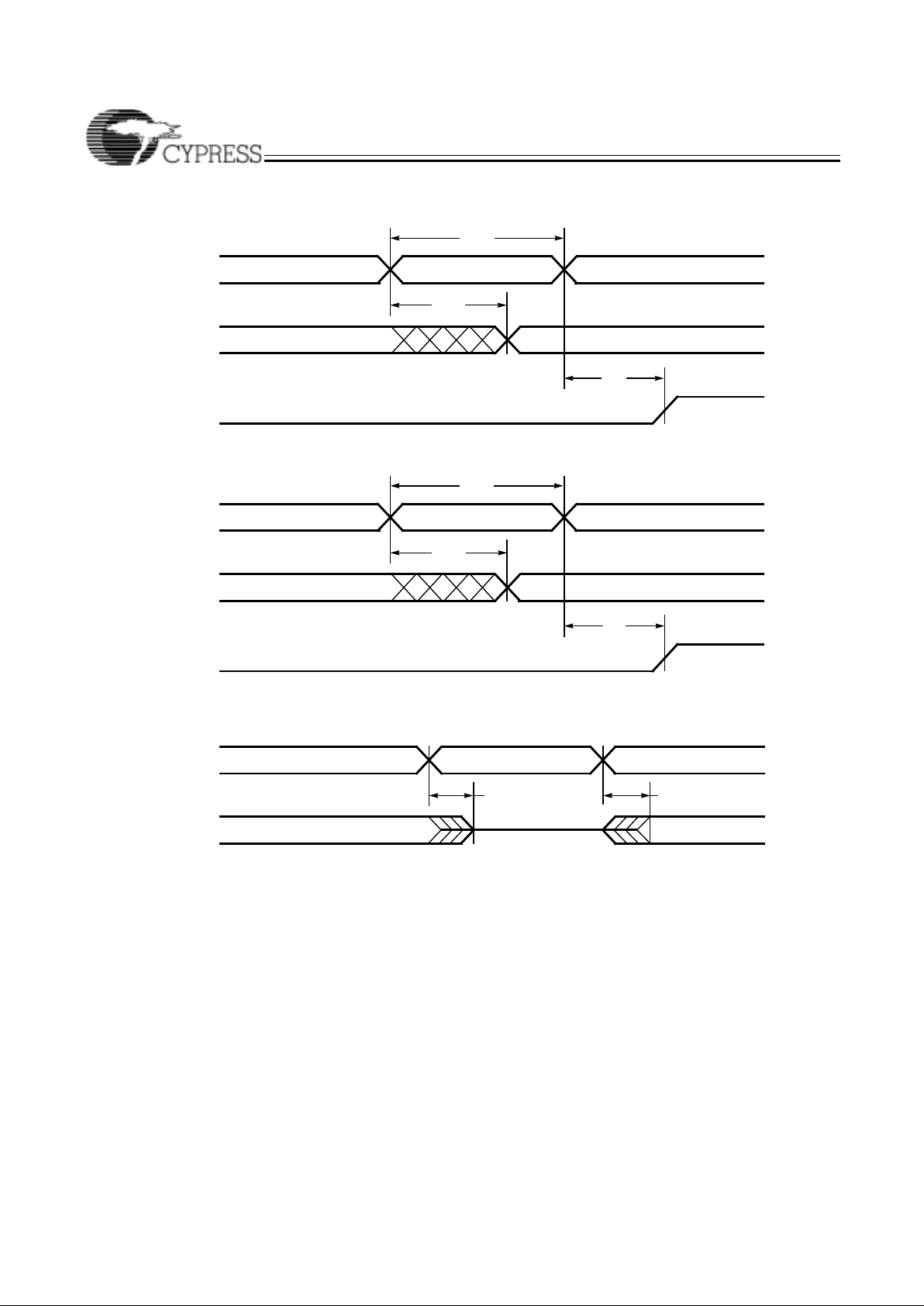
Note:
19. Only applicable to the 5V devices.
t
PD
INPUT
COMBINATORIAL
OUTPUT
Combinatorial Output

Ultra37000 CPLD Fami
ly
Document #: 38-03007 Rev. *B Page 21 of 63
Switching Waveforms (continued)
Registered Output with Synchronous Clocking
t
S
INPUT
SYNCHRONOUS
t
CO
REGISTERED
OUTPUT
t
H
SYNCHRONOUS
t
WL
t
WH
t
CO2
REGISTERED
OUTPUT
CLOCK
CLOCK
Registered Output with Product Term Clocking
t
SPT
INPUT
PRODUCT TER M
t
COPT
REGISTERED
OUTPUT
t
HPT
CLOCK
Input Going Through the Array
Registered Output with Product Term Clocking
t
ISPT
INPUT
PRODUCT TER M
t
CO2PT
REGISTERED
OUTPUT
t
IHPT
CLOCK
Input Coming From Adjacent Buried Register

Ultra37000 CPLD Fami
ly
Document #: 38-03007 Rev. *B Page 22 of 63
Switching Waveforms (continued)
Latched Output
t
SL
INPUT
LATCH ENABLE
t
CO
LATCHED
OUTPUT
t
HL
t
PDL
Registered Input
t
IS
REGISTERED
INPUT
INPUT REGISTER
CLOCK
t
ICO
COMBINATORIAL
OUTPUT
t
IH
CLOCK
t
WL
t
WH
Clock to Clock
INPUT REGISTER
CLOCK
OUTPUT
REGISTER CLOCK
t
SCS
t
ICS

Ultra37000 CPLD Fami
ly
Document #: 38-03007 Rev. *B Page 23 of 63
Switching Waveforms (continued)
Latched Input
t
IS
LATCHED INPUT
LATCH ENABLE
t
ICO
COMBINATORIAL
OUTPUT
t
IH
t
PDL
t
WL
t
WH
LATCH ENABLE
Latched Input and Output
t
ICS
LATCHED INPUT
OUTPUT LATCH
ENABLE
LATCHED
OUTPUT
t
PDLL
LATCH ENABLE
t
WL
t
WH
t
ICOL
INPUT LATCH
ENABLE
t
SL
t
HL
Ultra37000 CPLD Fami
ly
Document #: 38-03007 Rev. *B Page 24 of 63
Switching Waveforms (continued)
Asynchronous Reset
INPUT
t
RO
REGISTERED
OUTPUT
CLOCK
t
RR
t
RW
Asynchronous Preset
INPUT
t
PO
REGISTERED
OUTPUT
CLOCK
t
PR
t
PW
Output Enable/Disable
INPUT
t
ER
OUTPUTS
t
EA

Ultra37000 CPLD Fami
ly
Document #: 38-03007 Rev. *B Page 25 of 63
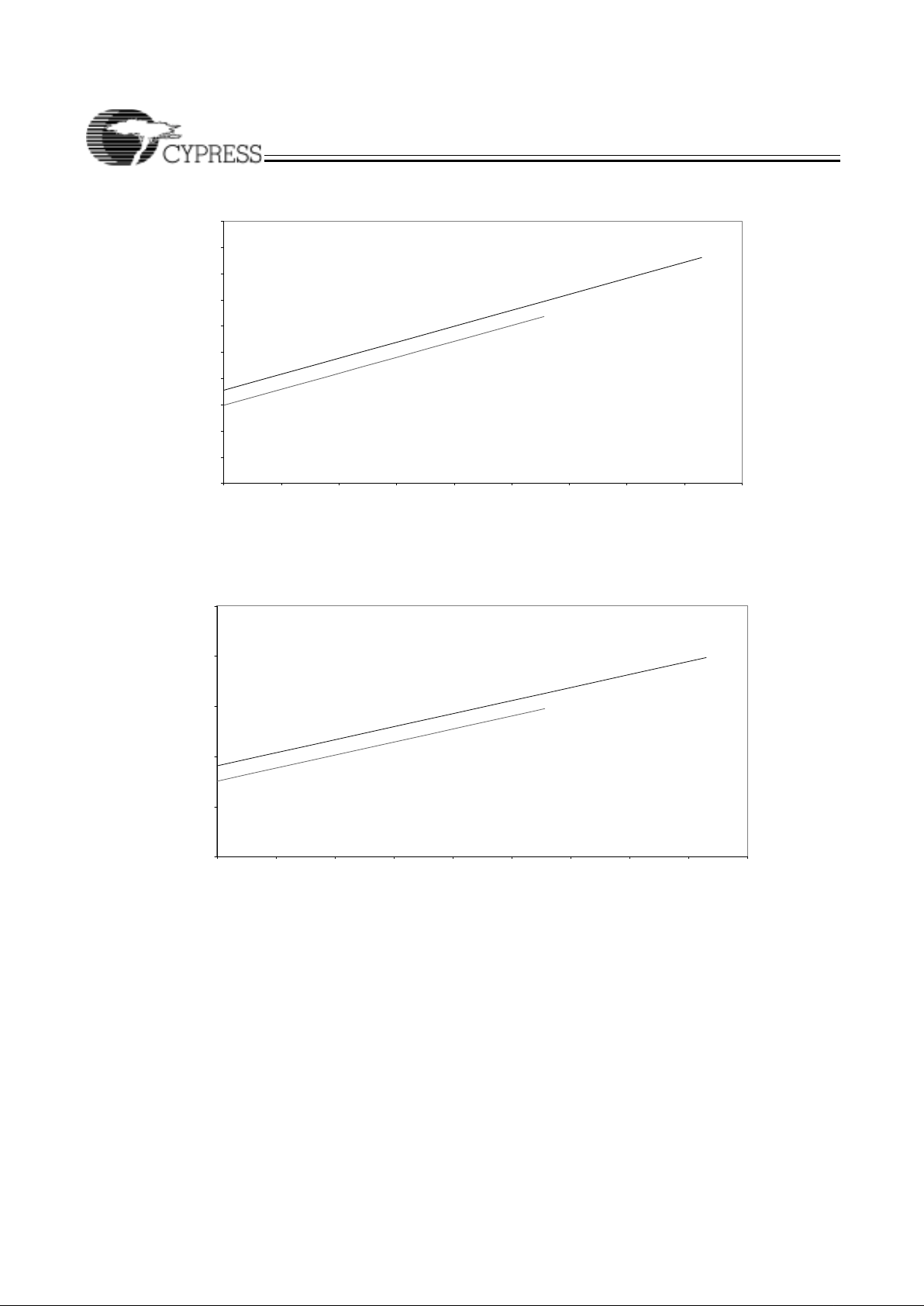
Power Consumption
Typical 5.0V Power Consumption
CY37032
CY37064
0
10
20
30
40
50
60
0 50 100 150 200 250
Frequency (MHz)
Icc (mA)
High Speed
Low Power
The typical pattern is a 16-bit up counter, per logic block, with outputs disabled.
V
CC
= 5.0V, TA = Room Temperature
The typical pattern is a 16-bit up counter, per logic block, with outputs disabled.
V
CC
= 5.0V, TA = Room Temperature
0
10
20
30
40
50
60
70
80
90
0 20 40 60 80 100 120 14 0 160 180
Frequency (MHz)
Icc (mA)
Low Power
High Speed

Ultra37000 CPLD Fami
ly
Document #: 38-03007 Rev. *B Page 26 of 63
CY37128
CY37192
Typical 5.0V Power Consumption (continued)
0
20
40
60
80
100
120
140
160
0 20 40 60 80 100 120 140 160 180
Frequency (MHz)
Icc (mA)
Low Power
High Speed
The typical pattern is a 16-bit up counter, per logic block, with outputs disabled.
V
CC
= 5.0V, TA = Room Temperature
0
50
100
150
200
250
300
0 20 40 60 80 100 120 140 160 180
Frequency (MHz)
Icc (mA)
Low Power
High Speed
The typical pattern is a 16-bit up counter, per logic block, with outputs disabled.
V
CC
= 5.0V, TA = Room Temperature

Ultra37000 CPLD Fami
ly
Document #: 38-03007 Rev. *B Page 27 of 63
CY37256
CY37384
Typical 5.0V Power Consumption (continued)
0
50
100
150
200
250
300
0 20 40 60 80 100 120 140 160 180
Frequency (MHz)
Icc (mA)
Low Power
High Speed
The typical pattern is a 16-bit up counter, per logic block, with outputs disabled.
V
CC
= 5.0V, TA = Room Temperature
0
50
100
150
200
250
300
350
400
450
500
0 20406080100120140160
Frequency (MHz)
Icc (mA)
Low Power
High Speed
The typical pattern is a 16-bit up counter, per logic block, with outputs disabled.
V
CC
= 5.0V, TA = Room Temperature

Ultra37000 CPLD Fami
ly
Document #: 38-03007 Rev. *B Page 28 of 63
CY37512
Typical 5.0V Power Consumption (continued)
0
100
200
300
400
500
600
0 20 40 60 80 100 120 140 160
Frequency (MHz)
Icc (mA)
Low Power
High Speed
The typical pattern is a 16-bit up counter, per logic block, with outputs disabled.
V
CC
= 5.0V, TA = Room Temperature
Typical 3.3V Power Consumption
CY37032V
0
5
10
15
20
25
30
0 20 40 60 80 100 120 140 160
Frequency (MHz)
Icc (mA)
Low Power
High Speed
The typical pattern is a 16-bit up counter, per logic block, with outputs disabled.
V
CC
= 3.3V, TA = Room Temperature

Ultra37000 CPLD Fami
ly
Document #: 38-03007 Rev. *B Page 29 of 63
CY37064V
CY37128V
Typical 3.3V Power Consumption (continued)
0
5
10
15
20
25
30
35
40
45
0 20406080100120140
Frequency (MHz)
Icc (mA)
Low Power
High Speed
The typical pattern is a 16-bit up counter, per logic block, with outputs disabled.
V
CC
= 3.3V, TA = Room Temperature
0
10
20
30
40
50
60
70
80
0 20 40 60 80 100 120 140
Frequency (MHz)
Icc (mA)
Low Power
High Speed
The typical pattern is a 16-bit up counter, per logic block, with outputs disabled.
V
CC
= 3.3V, TA = Room Temperature

Ultra37000 CPLD Fami
ly
Document #: 38-03007 Rev. *B Page 30 of 63
CY37192V
CY37256V
Typical 3.3V Power Consumption (continued)
0
20
40
60
80
100
120
0 20 40 60 80 100 120
Frequency (M Hz)
Icc (mA)
Low Power
High Speed
The typical pattern is a 16-bit up counter, per logic block, with outputs disabled.
V
CC
= 3.3V, TA = Room Temperature
0
20
40
60
80
100
120
140
0 20 40 60 80 100 120
Frequency (M Hz)
Icc (mA)
Low Power
High Speed
The typical pattern is a 16-bit up counter, per logic block, with outputs disabled.
V
CC
= 3.3V, TA = Room Temperature
Ultra37000 CPLD Fami
ly
Document #: 38-03007 Rev. *B Page 31 of 63
CY37384V
CY37512V
Typical 3.3V Power Consumption (continued)
0
20
40
60
80
100
120
140
160
180
200
0 102030405060708090
Frequency (MHz)
Icc (mA)
Low Power
High Speed
The typical pattern is a 16-bit up counter, per logic block, with outputs disabled.
V
CC
= 3.3V, TA = Room Temperature
0
50
100
150
200
250
0 102030405060708090
Frequency (MHz)
Icc (mA)
Low Power
High Speed
The typical pattern is a 16-bit up counter, per logic block, with outputs disabled.
V
CC
= 3.3V, TA = Room Temperature
Ultra37000 CPLD Fami
ly
Document #: 38-03007 Rev. *B Page 32 of 63
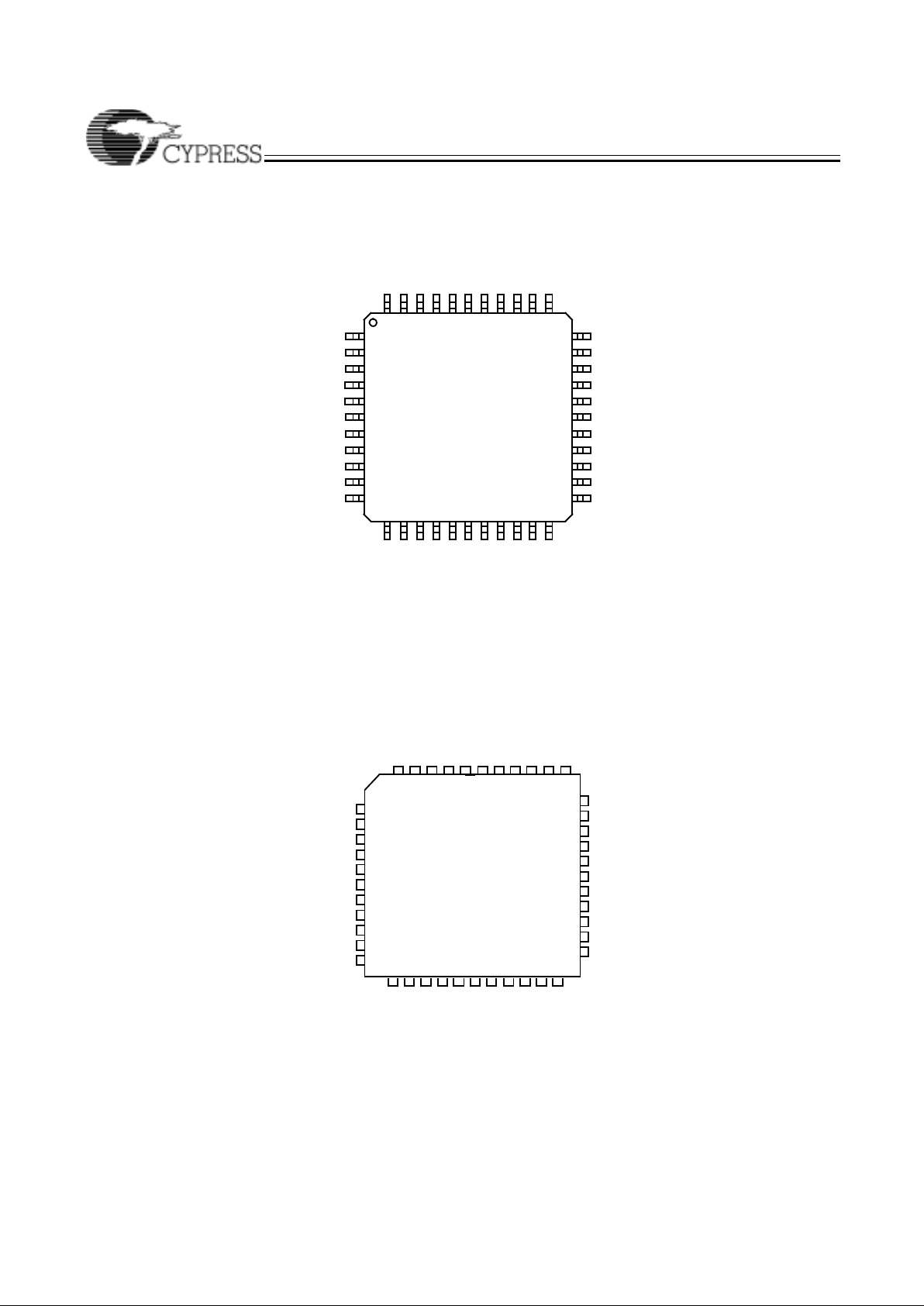
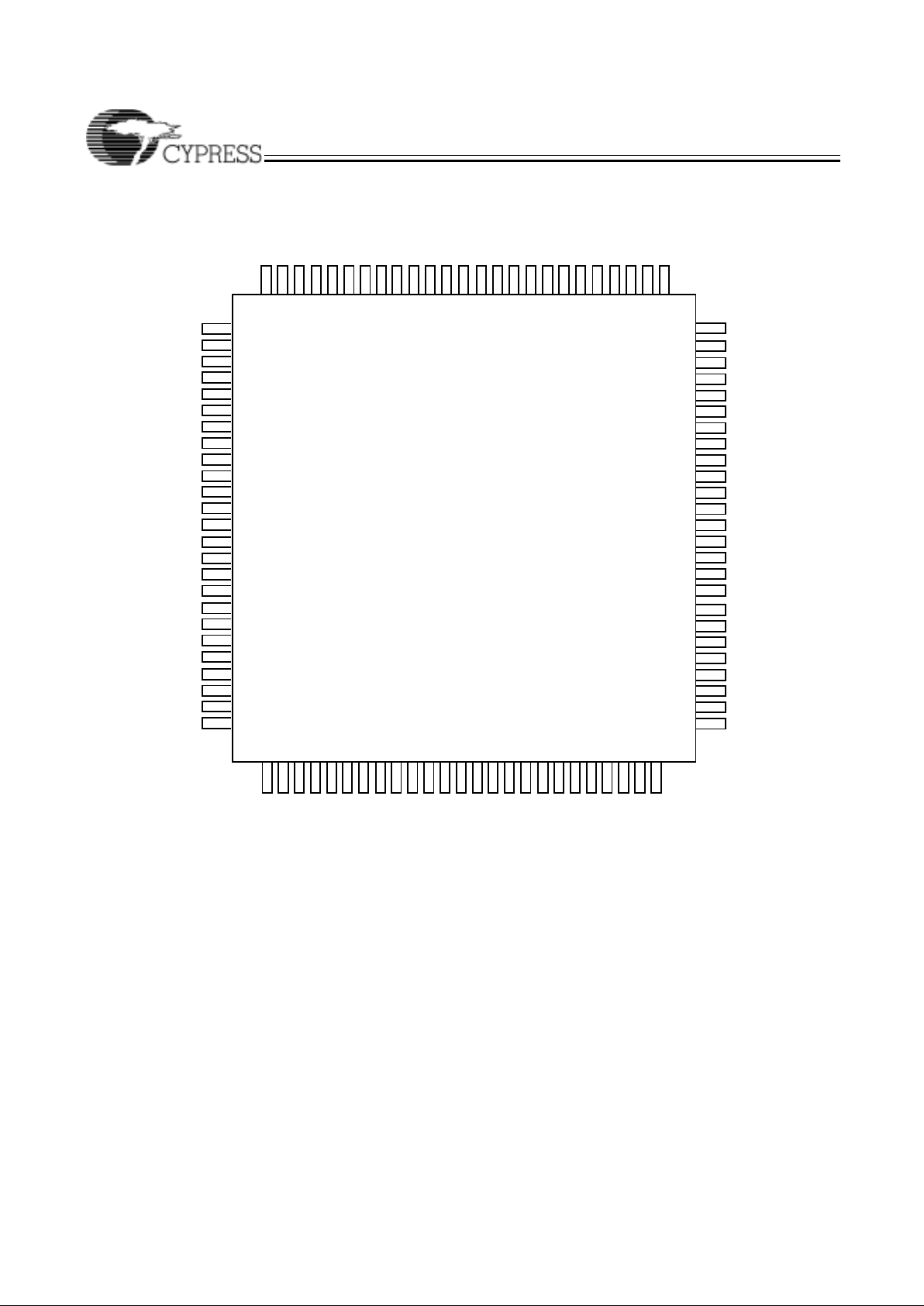
Pin Configurations
[20]
Note:
20. For 3.3V versions (Ultra37000V), V
CCO
= VCC.
44-pin TQFP (A44)
Top View
I/O
2
GND
V
CCO
I/O3I/O
4
I/O1I/O
0
I/O29I/O30I/O
31
I/O
28
I/O27/TDI
I/O
26
I/O
25
I/O
24
CLK1/I
4
GND
I
3
CLK3/I
2
I/O
23
I/O
22
I/O
21
GND
I/O
20
V
CC
I/O18I/O17I/O
16
I/O
15
I/O
14
I/O
12
I/O5/TCK
I/O
6
I/O
7
CLK2/I
0
GND
CLK
0
/I
1
I/O
8
I/O
9
I/O
10
I/O
11
8
9
7
10
11
3
4
2
5
6
1
18 19 20 222113 14 15 171612
31
30
29
32
33
26
25
24
27
28
23
44 43 42 4041 39 38 37 3536 34
I/O
13
/TMS
I/O
19
/TDO
JTAG
EN
44-pin PLCC (J67) / CLCC (Y67)
Top View
I/O27/TDI
I/O
26
I/O
25
I/O
24
CLK1/I
4
GND
I
3
CLK3/I
2
I/O
23
I/O
22
I/O
21
I/O5/TCK
I/O
6
I/O
7
CLK2/I
0
JTAG
EN
GND
CLK
0
/I
1
I/O
8
I/O
9
I/O
10
I/O
11
GND
I/O
20
I/O
2
GND
V
CCO
V
CC
I/O3I/O
4
I/O1I/O
0
I/O29I/O30I/O
31
I/O
28
I/O
19
I/O
18
I/O17I/O
16
I/O
15
I/O
14
I/O
13
I/O
12
65 34 2
8
9
7
10
11
44
18
15
16
14
13
12
17
19 20 2221 23 24 2726 2825
31
30
29
32
33
34
39
37
38
36
35
43 42 4041
/TMS
/TDO
1

Ultra37000 CPLD Fami
ly
Document #: 38-03007 Rev. *B Page 33 of 63
Note:
21. This pin is a N/C, but Cypress recommends that you connect it to V
CC
to ensure future compatibility.
Pin Configurations
[20]
(continued)
48-ball Fine-Pitch BGA (BA50)
T op V iew
12345678
AI/O
5
TCK
V
CC
I/O3I/O1I/O31I/O30VCCI/O27
TDI
BV
CC
I/O4I/O2I/O0I/O29I/O28I/O26CLK1/ I
4
CCLK2/ I0I/O7I/O6GND GND I/O25I/O
24I3
DJTAGENI/O8I/O9GND GND I/O22I/O23CLK3/ I
2
ECLK0/ I1I/O12I/O11I/O10I/O16I/O20I/O21V
CC
FI/O
13
TMS
VCCI/O14I/O15I/O17I/O18VCCI/O19
TDO
I/O
I/O
14
I/O
15
I/O
48
Top View
84-lead PLCC (J83) / CLCC (Y84)
98 67 5
13
14
12
11
4948
58
59
60
23
24
26
25
27
15
16
4746
43
28
33
20
21
19
18
17
22
34
3736
38
42414340
66
65
63
64
62
61
67
68
69
74
72
73
71
70
84 8182 80 79
GND
I/O
GND
I/O
I/O
I/O
I/O
I/O
I/O
I/O
GND
I/O
55
I/O
54
/TDI
I/O
53
I/O
52
I/O
51
GND
I/O
49
CLK3/I
4
V
CCO
CLK2/I
3
I/O
45
I/O
44
GND
I/O
I/O
8
I/O
9
I/O
10
/TCK
I/O
11
I/O
12
I/O
13
CLK0/I
0
V
CCO
CLK1/I
1
I/O
16
I/O
17
I/O
18
I/O
19
I/O
20
53525150
30
29
31
32
I/O
I/O
I/O
I/O
54
55
56
57
I/O
43
I/O
42
I/O
41
I/O
40
7778 76 75
I/O
21
I/O
22
I/O
23
GND
I/O
I/O
50
I/O
47
I/O
46
GND
24
I/O
25
/TMS
I/O27I/O28I/O29I/O30I/O
31
V
CCO
V
CC
I/O32I/O33I/O34I/O35I/O36I/O
37
I/O
38
I/O
39
GND
I
2
7
6
543
2
1
V
CCO
I/O
0
V
CC
63
I/O
62616059585756
JTAG
EN
I/O
26
/TDO
10
35 39 44 45
83
2
1
[2
Ultra37000 CPLD Fami
ly
Document #: 38-03007 Rev. *B Page 34 of 63
Pin Configurations
[20]
(continued)
Top View
100-lead TQFP (A100)
100 9798 96
2
3
1
4241
59
60
61
12
13
15
14
16
4
5
4039
95 94
17
26
9
10
8
7
6
11
27 28 3029 31 32 3534 36 3833
67
66
64
65
63
62
68
69
70
75
73
74
72
71
89 88 8687 8593 92 84
TDI
NC
V
CCO
I/O
55
I/O
54
I/O
53
I/O
52
CLK3/I
4
I/O
50
I/O
48
GND
NC
I/O
47
I/O
46
I/O
49
GND
TMS
TCK
GND
I/O
8
I/O
9
I/O
10
I/O
11
I/O
15
V
CCO
GND
CLK
1/I1
I/O
16
I/O
17
CLK0/I
0
9091
I/O
51
V
CCO
CLK2/I
3
I/O
14
N/C
I/O
12
I/O
13
I/O
45
I/O
44
I/O
43
I/O
42
I/O
41
I/O
40
GND
NC
GND
NC
I/O
18
I/O
19
I/O
20
I/O
21
I/O
22
I/O
23
V
CCO
NC
18
19
20
21
22
23
24
25
83 82 81 80 79 78 77 76
58
57
56
55
54
53
52
51
43 44 45 46 48
49 50
GND
I/O24I/O25I/O26I/O27I/O28I/O29I/O30I/O
31
V
CCO
V
CC
I/O32I/O33I/O34I/O35I/O36I/O37I/O38I/O
39
I
2
NC
V
CCO
TDO
I/O
I/O
GND
I/O
I/O
I/O
I/O
I/O
I/O
I/O
I/O
I/O
I/O
I/O
I/O
7654321
V
CCO
I/O
0
V
CC
NC
63
I/O
62616059585756
V
CCO
N/C
99
37
47
[21 ]
Ultra37000 CPLD Fami
ly
Document #: 38-03007 Rev. *B Page 35 of 63
Pin Configurations
[20]
(continued)
100-ball Fine-Pitch BGA (BB100) for CY37064V
Top View
100-ball Fine-Pitch BGA (BB100) for CY37128V
Top View
12345678910
A NC NC I/O
7
I/O5I/O2I/O62I/O60I/O58I/O57I/O
56
BI/O9I/O8I/O6I/O4I/O1I/O63VCCI/O59I/O55NC
CI/O10TCK VCCI/O3NC NC I/O61VCCTDI I/O
54
D I/O11NC I/O12I/O13I/O0NC I/O51I/O52CLK
3
/ I
4
I/O
53
EI/O14CLK
0
/ I
0
I/O15NC GND GND I/O48I/O49CLK
2
/ I
3
I/O
50
FI/O17NC NC I/O16GND GND NC NC I2I/O
47
GI/O22CLK
1
/ I
1
I/O21I/O19I/O18I/O46I/O45I/O44NC I/O
43
HI/O23TMS VCCI/O20NC I/O32I/O42VCCTDO I/O
41
J NC I/O26I/O28NC I/O31I/O33I/O35I/O37I/O39I/O
40
KI/O24I/O25I/O27I/O29I/O30I/O34I/O36I/O38NC NC
12345678910
A NC I/O
9
I/O8I/O6I/O3I/O76I/O74I/O72I/O71I/O
70
B I/O11I/O10I/O7I/O5I/O2I/O77VCCI/O73I/O68I/O
69
CI/O12I/O
13
TCK
VCCI/O4I/O1I/O78I/O75VCCI/O
67
TDI
I/O
66
DI/O14NC I/O15I/O16I/O0I/O79I/O63I/O64CLK
3
/ I
4
I/O
65
EI/O17CLK
0
/ I
0
I/O18I/O19GND GND I/O60I/O61CLK
2
/ I
3
I/O
62
FI/O
22
JTAG
EN
I/O21I/O20GND GND I/O59I/O58I2I/O
57
GI/O27CLK
1
/ I
1
I/O26I/O24I/O23I/O56I/O55I/O54NC I/O
53
HI/O28I/O
33
TMS
VCCI/O25I/O39I/O40I/O52VCCI/O
47
TDO
I/O
51
JI/O29I/O32I/O35VCCI/O38I/O41I/O43I/O45I/O48I/O
50
KI/O30I/O31I/O34I/O36I/O37I/O42I/O44I/O46I/O49NC

Ultra37000 CPLD Fami
ly
Document #: 38-03007 Rev. *B Page 36 of 63
Pin Configurations
[20]
(continued)
I/O
77
124
123
122
121
120
119
118
117
116
115
114
113
112
111
110
109
108
107
106
105
104
103
102
101
100
99
98
97
96
95
94
93
92
91
90
89
88
87
86
85
43
44
16045159461584715748156491555015451153521525315154150551495614857147581465914560144611436214263141
6465666768
1406913970138711377213673135741347513376132771317813079129801288112782126
160-Lead TQFP (A160) / CQFP (U162)
125
84
83
42
GND
I/O
16
I/O
17
I/O
18
I/O
19
I/O20/TCK
I/O
21
I/O
22
I/O
23
I/O
24
I/O
25
I/O
26
I/O
27
I/O
28
I/O
29
I/O
30
I/O
31
I/O
32
I/O
33
I/O
34
I/O
35
I/O
36
I/O
37
I/O
38
I/O
39
I/O
40
I/O
41
I/O
42
I/O
43
I/O
44
I/O
45
I/O
46
I/O
47
GND
CLK
0/I0
V
CCO
GND
CLK
1/I1
GND
GND
GND
GND
GND
V
CCO
I/O48I/O49I/O50I/O51I/O53I/O54I/O55I/O56I/O57I/O58I/O59I/O60I/O61I/O62I/O
63
I
2
V
CCO
V
CC
I/O64I/O65I/O66I/O67I/O68I/O69I/O70I/O71I/O72I/O73I/O74I/O75I/O78I/O
79
V
CCO
GND
I/O
80
I/O
81
I/O
82
I/O
83
I/O
84
I/O
85
I/O
86
I/O
87
GND
I/O
88
I/O
89
I/O
90
I/O
91
I/O
92
I/O
93
I/O
94
I/O
95
I/O
96
I/O
97
I/O
98
I/O
99
I/O
100
I/O
101
I/O
102
I/O
103
GND
GND
CLK2/I
3
V
CCO
CLK3/I
4
I/O
104
I/O
105
I/O
106
I/O
107
I/O
108
/TDI
I/O
109
I/O
110
I/O
111
V
CCO
GND
GND
V
CC
GND
I/O
112
GND
V
CCO
V
CCO
I/O
113
I/O
114
I/O
115
I/O
116
I/O
117
I/O
118
I/O
119
I/O
120
I/O
121
I/O
122
I/O
123
I/O
124
I/O
125
I/O
126
I/O
127
I/O0I/O1I/O2I/O3I/O4I/O5I/O6I/O
7
I/O8I/O9I/O10I/O11I/O12I/O13I/O14I/O
15
JTAG
EN
I/O
52
/TMS
I/O
76
/TDO
2
3
4
5
6
7
8
9
10
11
12
13
14
15
16
17
18
19
20
21
22
23
24
25
26
27
28
29
30
31
32
33
34
35
36
37
38
39
40
1
41
for CY37128(V) and CY37256(V)
Top View
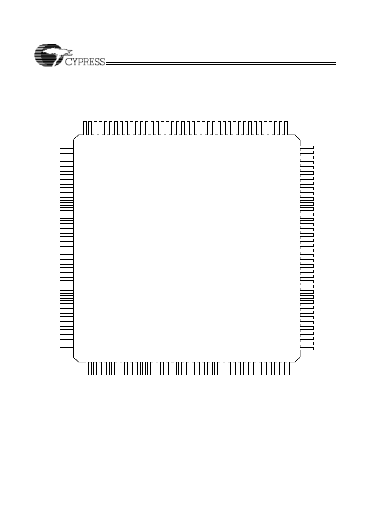
Ultra37000 CPLD Fami
ly
Document #: 38-03007 Rev. *B Page 37 of 63
Pin Configurations
[20]
(continued)
I/O
72
124
123
122
121
120
119
118
117
116
115
114
113
112
111
110
109
108
107
106
105
104
103
102
101
100
99
98
97
96
95
94
93
92
91
90
89
88
87
86
85
43
44
16045159461584715748156491555015451153521525315154150551495614857147581465914560144611436214263141
6465666768
1406913970138711377213673135741347513376132771317813079129801288112782126
160-Lead TQFP (A160) for CY37192(V)
125
84
83
42
GND
NC
I/O
16
I/O
17
I/O
18
TCK
I/O
19
I/O
20
I/O
21
I/O
22
I/O
23
I/O
24
I/O
25
I/O
26
I/O
27
I/O
28
I/O
29
I/O
30
I/O
31
I/O
32
I/O
33
I/O
34
I/O
35
I/O
36
I/O
37
I/O
38
I/O
39
I/O
40
I/O
41
I/O
42
I/O
43
I/O
44
I/O
45
GND
CLK
0/I0
V
CCO
GND
CLK
1/I1
GND
GND
GND
GND
GND
V
CCO
NC
I/O46I/O47I/O48I/O49I/O50I/O51I/O52I/O53I/O54I/O55I/O56I/O57I/O58I/O
59
I
2
V
CCO
V
CC
I/O60I/O61I/O62I/O63I/O64I/O65I/O66I/O67I/O68I/O69I/O70I/O71I/O73I/O
74
V
CCO
GND
NC
I/O
75
I/O
76
I/O
77
I/O
78
I/O
79
I/O
80
I/O
81
GND
I/O
82
I/O
83
I/O
84
I/O
85
I/O
86
I/O
87
I/O
88
I/O
89
I/O
90
I/O
91
I/O
92
I/O
93
I/O
94
I/O
95
I/O
96
I/O
97
GND
GND
CLK2/I
3
V
CCO
CLK3/I
4
I/O
98
I/O
99
I/O
100
I/O
101
TDI
I/O
102
I/O
103
I/O
104
V
CCO
GND
GND
V
CC
GND
NC
GND
V
CCO
V
CCO
I/O
105
I/O
106
I/O
107
I/O
108
I/O
109
I/O
110
I/O
111
I/O
112
I/O
113
I/O
114
I/O
115
I/O
116
I/O
117
I/O
118
I/O
119
I/O0I/O1I/O2I/O3I/O4I/O5I/O6I/O
7
I/O8I/O9I/O10I/O11I/O12I/O13I/O14I/O
15
NC
TMS
TDO
2
3
4
5
6
7
8
9
10
11
12
13
14
15
16
17
18
19
20
21
22
23
24
25
26
27
28
29
30
31
32
33
34
35
36
37
38
39
40
1
41
Top View

Ultra37000 CPLD Fami
ly
Document #: 38-03007 Rev. *B Page 38 of 63
Pin Configurations
[20]
(continued)
I/O
152
I/O
154
I/O
153
2
3
4
5
6
7
8
9
10
11
12
13
14
15
16
17
18
19
20
21
22
23
24
25
26
27
28
29
30
31
32
33
34
35
36
37
38
39
40
1
41
42
43
44
45
46
47
48
49
50
51
52
206
205
204
203
202
201
200
199
198
197
196
195
194
193
192
191
190
189
188
187
186
185
184
183
182
181
180
179
178
177
176
175
174
173
172
171
170
169
168
208
167
166
165
164
163
162
161
160
159
158
157
54555657585960616263646566676869707172737475767778798081828384858687888990
91539293949596979899100
101
102
103
154
153
152
151
150
149
148
147
146
145
144
143
142
141
140
139
138
137
136
135
134
133
132
131
130
129
128
127
126
125
124
123
122
121
120
119
118
117
116
155
115
114
113
112
111
110
109
108
107
106
105
156
104
207
208-Lead PQFP (N208) / CQFP (U208)
Top View
I/O
139
I/O
138
I/O
137
I/O
136
I/O
135
TDI
I/O
134
I/O
133
I/O
132
I/O
131
I/O
130
GND
I/O
129
I/O
128
I/O
127
I/O
126
I/O
125
I/O
124
I/O
123
I/O
122
I/O
121
I/O
120
CLK3/
I
4
V
CC
GND
V
CCO
GND
CLK2/
I
3
I/O
119
I/O
118
I/O
117
I/O
116
I/O
115
NC
I/O
114
I/O
113
I/O
112
I/O
111
I/O
110
V
CCO
GND
I/O
109
I/O
108
I/O
107
I/O
106
I/O
105
I/O
104
I/O
103
I/O
102
I/O
101
I/O
100
GND
I/O61I/O62I/O63I/O
64
TMS
I/O65I/O66I/O67I/O68I/O69GND
I/O70I/O71I/O72I/O73I/O
74
NC
I/O75I/O76I/O77I/O78I/O
79
I
2
V
CC0
GND
V
CC
I/O80I/O81I/O82I/O83I/O84I/O85I/O86I/O87I/O88I/O89GND
I/O90I/O
91
GND
I/O92I/O93I/O94GND
TDO
I/O95I/O96I/O97I/O
98
I/O99
V
CC0
I/O
60
I/O
21
I/O
22
I/O
23
I/O
24
TCK
I/O
25
I/O
26
I/O
27
I/O
28
I/O
29
GND
I/O
30
I/O
31
I/O
32
I/O
33
I/O
34
NC
I/O
35
I/O
36
I/O
37
I/O
38
I/O
39
CLK0/I
0
V
CCO
GND
NC
CLK1/I
1
I/O
40
I/O
41
I/O
42
I/O
43
I/O
44
I/O
45
I/O
46
I/O
47
I/O
48
I/O
49
GND
I/O
50
I/O
20
I/O
51
I/O
52
I/O
53
I/O
54
NC
I/O
55
I/O
56
I/O
57
I/O
58
I/O
59
V
CC0
GND
V
CC0
I/O19I/O18I/O17I/O16I/O15NC
I/O14I/O13I/O12I/O11I/O10GND
I/O9I/O8I/O7I/O6I/O5I/O4I/O3I/O2I/O1I/O0V
CC0
GND
VCCNC
I/O
159
I/O
158
I/O
157
I/O
156
I/O
155
NC
I/O
151
I/O
150
V
CC
GND
I/O
149
I/O
148
I/O
147
I/O
146
I/O
145
I/O
144
I/O
143
I/O
142
I/O
141
I/O
140
NC
GND
Ultra37000 CPLD Fami
ly
Document #: 38-03007 Rev. *B Page 39 of 63
Pin Configurations
[20]
(continued)
256-Ball PBGA (BG256)
T op V iew
1234567891011121314151617181920
A GND I/O
21
NC I/O16I/O12I/O9I/O7I/O4I/O0I/O
190
I/O
189
I/O
186
I/O
182
NC I/O
178
I/O
175
NC NC I/O
169
I/O
168
A
B I/O
23
I/O20I/O19I/O18I/O15I/O11I/O8I/O5I/O1I/O
191
I/O
187
I/O
185
I/O
181
NC NC I/O
174
I/O
171
I/O
170
NC I/O
166
B
C NC NC I/O
22
NC I/O17I/O14I/O10I/O6I/O2NC I/O
188
I/O
184
I/O
180
I/O
179
I/O
176
I/O
173
I/O
172
I/O
167
I/O
165
I/O
162
C
D I/O
24
NC NC GND NC V
CCO
I/O13GND I/O3NC VCCI/O
183
GND I/O
177VCCO
NC GND I/O
164
TDI I/O
160
D
E I/O
27
I/O26I/O25NC I/O
163
I/O
161
I/O
159
I/O
156
E
F I/O
30
TCK I/O28V
CCO
V
CCO
I/O
158
NC I/O
154
F
G I/O33I/O32I/O31I/O
29
I/O
157
I/O
155
I/O
153
I/O
152
G
H I/O
35
NC I/O34GND GND GND GND GND GND GND GND I/O
151
I/O
150
I/O
149
H
J I/O
39
I/O38I/O37I/O
36
GND GND GND GND GND GND I/O
148
I/O
147
I/O
146
I/O
145
J
K I/O
42
I/O40I/O41V
CC
GND GND GND GND GND GND I/O
144
CLK3/I4NC NC K
L I/O43I/O44I/O45I/O
46
GND GND GND GND GND GND VCCCLK2/I3I/O
143
NC L
M I/O
47
CLK0/I0CLK1/I1I/O
48
GND GND GND GND GND GND I/O
139
I/O
140
I/O
141
I/O
142
M
N I/O49I/O50I/O51GND GND GND GND GND GND GND GND I/O
136
I/O
137
I/O
138
N
P I/O52I/O53I/O55I/O
58
I/O
131
I/O
133
I/O
134
I/O
135
P
R I/O54I/O56I/O59V
CCO
V
CCO
I/O
130
NC I/O
132
R
T I/O57I/O60I/O62I/O
65
I/O
124
I/O
127
I/O
128
I/O
129
T
U I/O61I/O63I/O66GND I/O76V
CCO
I/O82GND I/O91VCCI/O98I/O
102
GND I/O
112VCCO
NC GND I/O
123
I/O
122
I/O
126
U
V I/O64I/O67I/O69I/O75I/O78I/O81I/O85I/O88I/O
92I2
I/O97I/O
101
I/O
105
I/O
109
I/O
113
TDO I/O
114
I/O
117
I/O
121
I/O
125
V
W I/O68I/O70I/O72I/O74I/O79I/O83I/O86I/O89I/O93I/O95I/O96I/O
100
I/O
104
I/O
107
I/O
110
NC NC I/O
115
I/O
118
I/O
120
W
Y I/O71I/O73I/O77TMS I/O80I/O84I/O87I/O90I/O94NC NC I/O99I/O
103
I/O
106
I/O
108
I/O
111
NC NC I/O
116
I/O
119
Y
1234567891011121314151617181920

Ultra37000 CPLD Fami
ly
Document #: 38-03007 Rev. *B Page 40 of 63
Pin Configurations
[20]
(continued)
256-Ball Fine-Pitch BGA (BB256)
T op V iew
12345678910111213141516
A GND GND I/O26I/O24I/O20VCCI/O11GND GND I/O
18
6
VCCI/O
17
7
I/O
17
2
I/O
16
7
GND GND
B GND I/O
27
I/O25I/O23I/O19I/O15I/O10GND GND I/O
18
5
I/O
18
1
I/O
17
6
I/O
17
1
I/O
16
6
I/O
16
5
GND
C I/O
29
I/O28NC I/O22I/O18I/O14I/O9I/O4I/O
19
1
I/O
18
4
I/O
18
0
I/O
17
5
I/O
17
0
NC I/O
16
3
I/O
16
4
D I/O32I/O31I/O30NC I/O17I/O13I/O8I/O3I/O
19
0
I/O
18
3
I/O
17
9
I/O
17
4
I/O
16
9
I/O
16
0
I/O
16
1
I/O
16
2
E I/O35I/O34I/O33I/O21I/O16I/O12I/O7I/O2I/O
18
9
VCCI/O
17
8
I/O
17
3
I/O
16
8
I/O
15
7
I/O
15
8
I/O
15
9
FVCCI/O38I/O37I/O36TCK VCCI/O6I/O1I/O
18
8
I/O
18
2
VCCTDI I/O
15
4
I/O
15
5
I/O
15
6
V
CC
G I/O43I/O42I/O41I/O40VCCI/O39I/O5I/O0I/O
18
7
I/O
14
8
I/O
14
9
CLK3
/I
4
I/O
15
0
I/O
15
1
I/O
15
2
I/O
15
3
H GND GND I/O47I/O46CLK0
/I
0
I/O45I/O44GND GND I/O
14
4
I/O
14
5
CLK2
/I
3
I/O
14
6
I/O
14
7
GND GND
J GND GND I/O51I/O50NC I/O49I/O48GND GND I/O
14
0
I/O
14
1
I2I/O
14
2
I/O
14
3
GND GND
K I/O57I/O56I/O55I/O54CLK1
/I
1
I/O53I/O52I/O91I/O96I/O
10
1
I/O
13
5
VCCI/O
13
6
I/O
13
7
I/O
13
8
I/O
13
9
LVCCI/O60I/O59I/O58TMS VCCI/O86I/O92I/O97I/O
10
2
VCCTDO I/O
13
2
I/O
13
3
I/O
13
4
V
CC
M I/O63I/O62I/O61I/O72I/O77I/O82VCCI/O93I/O98I/O
10
3
I/O
10
8
I/O
11
2
I/O
11
7
I/O
12
9
I/O
13
0
I/O
13
1
N I/O66I/O65I/O64I/O73I/O78I/O83I/O87I/O94I/O99I/O
10
4
I/O
10
9
I/O
11
3
NC I/O
12
6
I/O
12
7
I/O
12
8
P I/O68I/O67NC I/O74I/O79 I/O84I/O88I/O95I/O
10
0
I/O
10
5
I/O
11
0
I/O
11
4
I/O
11
8
NC I/O
12
4
I/O
12
5
R GND I/O69I/O70I/O75I/O80I/O85I/O89GND GND I/O
10
6
I/O
11
1
I/O
11
5
I/O
11
9
I/O
12
1
I/O
12
3
GND
T GND GND I/O71I/O76I/O81VCCI/O90GND GND I/O
10
7
VCCI/O
11
6
I/O
12
0
I/O
12
2
GND GND
Ultra37000 CPLD Fami
ly
Document #: 38-03007 Rev. *B Page 41 of 63
Pin Configurations
[20]
(continued)
352-Lead BGA (BG352)
Top View
1234567891011121314151617181920212223242526
A GND GND I/O
19
I/O15I/O13I/O34I/O31I/O28I/O25I/O10I/O7I/O4I/O1I/O
263
I/O
260
I/O
257
I/O
254
I/O
239
I/O
237
I/O
232
I/O
229
I/O
250
I/O
248
I/O
244
GND GND
B GND NC I/O18I/O17I/O14I/O35I/O32I/O29I/O26I/O11I/O8I/O5I/O2VCCI/O
261
I/O
258
I/O
255
I/O
252
I/O
234
I/O
231
I/O
228
I/O
249
I/O
246
I/O
245
I/O
240
GND
C I/O
23
I/O38I/O37I/O16I/O12I/O33I/O30I/O27I/O24I/O9I/O6I/O3I/O0I/O
262
I/O
259
I/O
256
I/O
253
I/O
238
I/O
235
I/O
233
I/O
230
I/O
251
I/O
247
I/O
225
I/O
224
I/O
227
D I/O39I/O40I/O36NC NC I/O21I/O20V
CCOVCCO
NC GND GND V
CCOVCCO
GND GND NC V
CCOVCCO
I/O
236
I/O
243
NC NC I/O
226
I/O
222
I/O
223
E I/O42TCK I/O41NC NC T DI I/O
221
I/O
220
F I/O45I/O44I/O43I/O
22
I/O
242
I/O
219
I/O
218
I/O
217
G I/O48I/O47I/O46I/O
63
I/O
241
I/O
216
I/O
215
I/O
214
H I/O49I/O50I/O51V
CCO
V
CCO
I/O
211
I/O
212
I/O
213
J I/O52I/O53I/O54V
CCO
V
CCO
I/O
208
I/O
209
I/O
210
K I/O55I/O56I/O57NC NC I/O
205
I/O
206
I/O
207
L I0 I/O59I/O58GND GND GND GND GND GND GND GND I/O
204
I4 I/O
197
M I/O61I/O60I1 GND GND GND GND GND GND GND GND I3 I/O
203
I/O
202
N I/O64VCCI/O62V
CCO
GND GND GND GND GND GND V
CCO
I/O
201
I/O
200
I/O
199
P I/O65I/O66I/O67V
CCO
GND GND GND GND GND GND V
CCO
I/O
196VCC
I/O
198
R I/O68I/O69I/O70GND GND GND GND GND GND GND GND I/O
193
I/O
194
I/O
195
T I/O71I/O84I/O85GND GND GND GND GND GND GND GND I/O
178
I/O
179
I/O
192
U I/O88I/O87I/O86NC NC I/O
177
I/O
176
I/O
175
V I/O91I/O90I/O89V
CCO
V
CCO
I/O
174
I/O
173
I/O
172
W I/O94I/O93I/O92V
CCO
V
CCO
I/O
171
I/O
170
I/O
169
Y I/O95I/O72I/O73I/O
110
I/O
153
I/O
190
I/O
191
I/O
168
AA I/O74I/O75I/O76I/O
111
I/O
152
I/O
187
I/O
188
I/O
189
AB I/O77I/O78I/O79N/C NC I/O
184
I/O
185
I/O
186
AC I/O81I/O80I/O
108
N/C NC I/O
112
I/O
113VCCOVCCO
NC GND GND V
CCOVCCO
GND GND NC V
CCOVCCO
I/O
150
I/O
151
NC NC I/O
155
I/O
183
I/O
182
AD I/O
109
I/O82I/O83I/O
117
I/O97I/O
100
I/O
102
I/O
105
I/O
120
I/O
123
I/O
126
I/O
129
I2 I/O
133
I/O
136
I/O
139
I/O
142
I/O
157
I/O
159
I/O
161
I/O
163
I/O
166
I/O
146
I/O
180
I/O
181
I/O
154
AE GND NC I/O
115
I/O
116
I/O
119
I/O98I/O
101
I/O
103
I/O
106
I/O
121
I/O
124
I/O
127VCC
I/O
130
I/O
134
I/O
137
I/O
140
I/O
143
I/O
160
I/O
162
I/O
165
I/O
144
I/O
147
I/O
148
NC GND
AF GND GND I/O
114
I/O
118
I/O96I/O99TMS I/O
104
I/O
107
I/O
122
I/O
125
I/O
128
I/O
131
I/O
132
I/O
135
I/O
138
I/O
141
I/O
156
I/O
158
TDO I/O
164
I/O
167
I/O
145
I/O
149
GND GND

Ultra37000 CPLD Fami
ly
Document #: 38-03007 Rev. *B Page 42 of 63
Pin Configurations
[20]
(continued)
400-Ball Fine-Pitch BGA (BB400)
T op V iew
A GNDGNDNCI/O17I/O16I/O14I/O29VCCI/O11GND GND I/O
25
7
VCCI/O
23
9
I/O
23
3
I/O
23
2
I/O
23
0
NC GND GND
B GND GND GND NC I/O15I/O13I/O28VCCI/O10GND GND I/O
25
6
VCCI/O
23
8
I/O
23
1
I/O
22
9
NC GND GND GND
C NC GND GND GND I/O
20
I/O12I/O27VCCI/O9GND GND I/O
25
5
VCCI/O
23
7
I/O
22
8
I/O
24
5
GND GND GND NC
DI/O44NC GND I/O21I/O19I/O18I/O26I/O25I/O8GND GND I/O
25
4
I/O
23
5
I/O
23
6
I/O
25
1
I/O
24
4
I/O
24
3
GND NC I/O
22
7
EI/O46I/O43I/O23I/O22NC I/O35I/O34I/O24I/O7I/O4I/O
26
3
I/O
25
3
I/O
23
4
I/O
25
0
I/O
24
8
NC I/O
24
1
I/O
24
2
I/O
22
5
I/O
22
6
FI/O47I/O45I/O42I/O41I/O40NC I/O33I/O32I/O6I/O3I/O
26
2
I/O
25
2
I/O
24
9
I/O
24
7
I/O
22
0
I/O
22
1
I/O
24
0
I/O
22
2
I/O
22
3
I/O
22
4
GI/O53I/O52I/O51I/O50I/O39I/O38I/O37I/O31I/O5I/O2I/O
26
1
VCCI/O
24
6
I/O
21
7
I/O
21
8
I/O
21
9
I/O
21
2
I/O
21
3
I/O
21
4
I/O
21
5
HVCCVCCVCCI/O49I/O48I/O36TCK VCCI/O30I/O1I/O
25
9
I/O
26
0
VCCTDI I/O
21
6
I/O
21
0
I/O
21
1
VCCVCCV
CC
JI/O59I/O58I/O57I/O56I/O55I/O54VCCI/O62I/O60I/O0I/O
25
8
I/O
20
2
I/O
20
3
CLK
3
/I
4
I/O
20
4
I/O
20
5
I/O
20
6
I/O
20
7
I/O
20
8
I/O
20
9
K GND GND GND GND I/O65I/O64CLK
0
/I
0
I/O63I/O61GND GND I/O
19
8
I/O
19
9
CLK
2 /I3
I/O
20
0
I/O
20
1
GND GND GND GND
L GND GND GND GND I/O69I/O68NC I/O67I/O66GND GND I/O
19
3
I/O
19
5
I2I/O
19
6
I/O
19
7
GND GND GND GND
MI/O89I/O88I/O87I/O86I/O85I/O84CLK
1
/I
1
I/O71I/O70I/O
12
6
I/O
13
2
I/O
19
2
I/O
19
4
VCCI/O
17
4
I/O
17
5
I/O
17
6
I/O
17
7
I/O
17
8
I/O
17
9
NVCCVCCVCCI/O91I/O90I/O72TMS VCCI/O
12
8
I/O
12
7
I/O
13
3
I/O
16
2
VCCTDO I/O
18
0
I/O
16
8
I/O
16
9
VCCVCCV
CC
PI/O95I/O94I/O93I/O92I/O75I/O74I/O73I/O
11
4
VCCI/O
12
9
I/O
13
4
I/O
13
7
I/O
16
3
I/O
18
1
I/O
18
2
I/O
18
3
I/O
17
0
I/O
17
1
I/O
17
2
I/O
17
3
RI/O80I/O79I/O78I/O
10
8
I/O77I/O76I/O
11
5
I/O
11
7
I/O
12
0
I/O
13
0
I/O
13
5
I/O
13
8
I/O
16
4
I/O
16
5
NC I/O
18
4
I/O
18
5
I/O
18
6
I/O
18
9
I/O
19
1
TI/O82I/O81I/O
11
0
I/O
10
9
NC I/O
11
6
I/O
11
8
I/O
10
2
I/O
12
1
I/O
13
1
I/O
13
6
I/O
13
9
I/O
15
6
I/O
16
6
I/O
16
7
NC I/O
15
4
I/O
15
5
I/O
18
7
I/O
19
0
UI/O83NC GND I/O
11
1
I/O
11
2
I/O
11
9
I/O
10
4
I/O
10
3
I/O
12
2
GND GND I/O
14
0
I/O
15
7
I/O
15
8
I/O
15
0
I/O
15
1
I/O
15
3
GND NC I/O
18
8
V NC GND GND GND I/O
11
3
I/O96I/O
10
5
VCCI/O
12
3
GND GND I/O
14
1
VCCI/O
15
9
I/O144I/O
15
2
GND GND GND NC
W GND GND GND NC I/O97I/O99I/O
10
6
VCCI/O
12
4
GND GND I/O
14
2
VCCI/O
16
0
I/O
14
5
I/O
14
7
NC GND GND GND
Y GNDGNDNCI/O98I/O
10
0
I/O
10
1
I/O
10
7
VCCI/O
12
5
GND GND I/O
14
3
VCCI/O
16
1
I/O
14
6
I/O
14
8
I/O
14
9
NC GND GND

Ultra37000 CPLD Fami
ly
Document #: 38-03007 Rev. *B Page 43 of 63
Ordering Information
5.0V Ordering Information
Macro-
cells
Speed
(MHz) Ordering Code
Package
Name Package Type
Operating
Range
32 200 CY37032P44-200AC A44 44-Lead Thin Quad Flat Pack Commercial
CY37032P44-200JC J67 44-Lead Plastic Leaded Chip Carrier
154 CY37032P44-154AC A44 44-Lead Thin Quad Flat Pack Commercial
CY37032P44-154JC J67 44-Lead Plastic Leaded Chip Carrier
CY37032P44-154AI A44 44-Lead Thin Quad Flat Pack Industrial
CY37032P44-154JI J67 44-Lead Plastic Leaded Chip Carrier
125 CY37032P44-125AC A44 44-Lead Thin Quad Flat Pack Commercial
CY37032P44-125JC J67 44-Lead Plastic Leaded Chip Carrier
CY37032P44-125AI A44 44-Lead Thin Quad Flat Pack Industrial
CY37032P44-125JI J67 44-Lead Plastic Leaded Chip Carrier
64 200 CY37064P44-200AC A44 44-Lead Thin Quad Flat Pack Commercial
CY37064P44-200JC J67 44-Lead Plastic Leaded Chip Carrier
CY37064P84-200JC J83 84-Lead Plastic Leaded Chip Carrier
CY37064P100-200AC A100 100-Lead Thin Quad Flat Pack
C Y 3 7 5 1 2 V P 4 0 0 - 8 3 B B C
C
ypress Semiconductor ID
F
amily Type
37 = Ultra37000 Family
M
acrocell Density
32 = 32 Macrocells 256 = 256 Macrocells
64 = 64 Macrocells 384 = 384 Macrocells
128 = 128 Macrocells 512 = 512 Macrocells
192 = 192 Macrocells
Speed
125 = 125 MHz
200 = 200 MHz 100 = 100 MHz
167 = 167 MHz 83 = 83 MHz
154 = 154 MHz 66 = 66 MHz
143 = 143 MHz
Package Type
A = Thin Quad Flat Pack (TQFP)
U = Ceramic Quad Flat Pack (CQFP)
N = Plastic Quad Flat Pack (PQFP)
NT = Thermally Enhanced Plastic Quad Flat Pack
(EQFP)
J = Plastic Leaded Chip Carrier (PLCC)
Y = Ceramic Leaded Chip Carrier (CLCC)
BG = Ball Grid Array (BGA)
BA = Fine-Pitch Ball Grid Array (FBGA)
0.8mm Lead Pitch
BB = Fine-Pitch Ball Grid Array (FBGA)
1.0mm Lead Pitch
Operating Conditions
Commercial 0°C to +70°C
Industrial -40°C to +85°C
Military -55°C to +125°C
O
perating Reference Voltage
V = 3.3V Supply Voltage
(5.0V if not specified)
P
in Count
P44 = 44 Leads
P48 = 48 Leads
P84 = 84 Leads
P100 = 100 Leads
P160 = 160 Leads
P208 = 208 Leads
P256 = 256 Leads
P352 = 352 Leads
P400 = 400 Leads

Ultra37000 CPLD Fami
ly
Document #: 38-03007 Rev. *B Page 44 of 63
64 154 CY37064P44-154AC A44 44-Lead Thin Quad Flat Pack Commercial
CY37064P44-154JC J67 44-Lead Plastic Leaded Chip Carrier
CY37064P84-154JC J83 84-Lead Plastic Leaded Chip Carrier
CY37064P100-154AC A100 100-Lead Thin Quad Flat Pack
CY37064P44-154AI A44 44-Lead Thin Quad Flat Pack Industrial
CY37064P44-154JI J67 44-Lead Plastic Leaded Chip Carrier
CY37064P84-154JI J83 84-Lead Plastic Leaded Chip Carrier
CY37064P100-154AI A100 100-Lead Thin Quad Flat Pack
5962-9951902QYA Y67 44-Lead Ceramic Leadless Chip Carrier Military
125 CY37064P44-125AC A44 44-Lead Thin Quad Flat Pack Commercial
CY37064P44-125JC J67 44-Lead Plastic Leaded Chip Carrier
CY37064P84-125JC J83 84-Lead Plastic Leaded Chip Carrier
CY37064P100-125AC A100 100-Lead Thin Quad Flat Pack
CY37064P44-125AI A44 44-Lead Thin Quad Flat Pack Industrial
CY37064P44-125JI J67 44-Lead Plastic Leaded Chip Carrier
CY37064P84-125JI J83 84-Lead Plastic Leaded Chip Carrier
CY37064P100-125AI A100 100-Lead Thin Quad Flat Pack
5962-9951901QYA Y67 44-Lead Ceramic Leadless Chip Carrier Military
128 167 CY37128P84-167JC J83 84-Lead Plastic Leaded Chip Carrier Commercial
CY37128P100-167AC A100 100-Lead Thin Quad Flat Pack
CY37128P160-167AC A160 160-Lead Thin Quad Flat Pack
125 CY37128P84-125JC J83 84-Lead Plastic Leaded Chip Carrier Commercial
CY37128P100-125AC A100 100-Lead Thin Quad Flat Pack
CY37128P160-125AC A160 160-Lead Thin Quad Flat Pack
CY37128P84-125JI J83 84-Lead Plastic Leaded Chip Carrier Industrial
CY37128P100-125AI A100 100-Lead Thin Quad Flat Pack
CY37128P160-125AI A160 160-Lead Thin Quad Flat Pack
5962-9952102QYA Y84 84-Lead Ceramic Leaded Chip Carrier Military
100 CY37128P84-100JC J83 84-Lead Plastic Leaded Chip Carrier Commercial
CY37128P100-100AC A100 100-Lead Thin Quad Flat Pack
CY37128P160-100AC A160 160-Lead Thin Quad Flat Pack
CY37128P84-100JI J83 84-Lead Plastic Leaded Chip Carrier Industrial
CY37128P100-100AI A100 100-Lead Thin Quad Flat Pack
CY37128P160-100AI A160 160-Lead Thin Quad Flat Pack
5962-9952101QYA Y84 84-Lead Ceramic Leaded Chip Carrier Military
192 154 CY37192P160-154AC A160 160-Lead Thin Quad Flat Pack Commercial
125 CY37192P160-125AC A160 160-Lead Thin Quad Flat Pack Commercial
CY37192P160-125AI A160 160-Lead Thin Quad Flat Pack Industrial
83 CY37192P160-83AC A160 160-Lead Thin Quad Flat Pack Commercial
CY37192P160-83AI A160 160-Lead Thin Quad Flat Pack Industrial
5.0V Ordering Information (continued)
Macro-
cells
Speed
(MHz) Ordering Code
Package
Name Package Type
Operating
Range

Ultra37000 CPLD Fami
ly
Document #: 38-03007 Rev. *B Page 45 of 63
256 154 CY37256P160-154AC A160 160-Lead Thin Quad Flat Pack Commercial
CY37256P208-154NC N208 208-Lead Plastic Quad Flat Pack
CY37256P256-154BGC BG256 256-Lead Ball Grid Array
125 CY37256P160-125AC A160 160-Lead Thin Quad Flat Pack Commercial
CY37256P208-125NC N208 208-Lead Plastic Quad Flat Pack
CY37256P256-125BGC BG256 256-Lead Ball Grid Array
CY37256P160-125AI A160 160-Lead Thin Quad Flat Pack Industrial
CY37256P208-125NI N208 208-Lead Plastic Quad Flat Pack
CY37256P256-125BGI BG256 256-Lead Ball Grid Array
5962-9952302QZC U162 160-Lead Ceramic Quad Flat Pack Military
83 CY37256P160-83AC A160 160-Lead Thin Quad Flat Pack Commercial
CY37256P208-83NC N208 208-Lead Plastic Quad Flat Pack
CY37256P256-83BGC BG256 256-Lead Ball Grid Array
CY37256P160-83AI A160 160-Lead Thin Quad Flat Pack Industrial
CY37256P208-83NI N208 208-Lead Plastic Quad Flat Pack
CY37256P256-83BGI BG256 256-Lead Ball Grid Array
5962-9952301QZC U162 160-Lead Ceramic Quad Flat Pack Military
384 125 CY37384P208-125NC N208 208-Lead Plastic Quad Flat Pack Commercial
CY37384P256-125BGC BG256 256-Lead Ball Grid Array
83 CY37384P208-83NC N208 208-Lead Plastic Quad Flat Pack Commercial
CY37384P256-83BGC BG256 256-Lead Ball Grid Array
CY37384P208-83NI N208 208-Lead Plastic Quad Flat Pack Industrial
CY37384P256-83BGI BG256 256-Lead Ball Grid Array
512 125 CY37512P208-125NC N208 208-Lead Plastic Quad Flat Pack Commercial
CY37512P256-125BGC BG256 256-Lead Ball Grid Array
CY37512P352-125BGC BG352 352-Lead Ball Grid Array
100 CY37512P208-100NC N208 208-Lead Plastic Quad Flat Pack Commercial
CY37512P256-100BGC BG256 256-Lead Ball Grid Array
CY37512P352-100BGC BG352 352-Lead Ball Grid Array
CY37512P208-100NI N208 208-Lead Plastic Quad Flat Pack Industrial
CY37512P256-100BGI BG256 256-Lead Ball Grid Array
CY37512P352-100BGI BG352 352-Lead Ball Grid Array
5962-9952502QZC U208 208-Lead Ceramic Quad Flat Pack Military
83 CY37512P208-83NC N208 208-Lead Plastic Quad Flat Pack Commercial
CY37512P256-83BGC BG256 256-Lead Ball Grid Array
CY37512P352-83BGC BG352 352-Lead Ball Grid Array
CY37512P208-83NI N208 208-Lead Plastic Quad Flat Pack Industrial
CY37512P256-83BGI BG256 256-Lead Ball Grid Array
CY37512P352-83BGI BG352 352-Lead Ball Grid Array
5962-9952501QZC U208 208-Lead Ceramic Quad Flat Pack Military
5.0V Ordering Information (continued)
Macro-
cells
Speed
(MHz) Ordering Code
Package
Name Package Type
Operating
Range

Ultra37000 CPLD Fami
ly
Document #: 38-03007 Rev. *B Page 46 of 63
3.3V Ordering Information
Macro-
cells
Speed
(MHz) Ordering Code
Package
Name Package Type
Operating
Range
32 143 CY37032VP44-143AC A44 44-Lead Thin Quad Flat Pack Commercial
CY37032VP44-143JC J67 44-Lead Plastic Leaded Chip Carrier
CY37032VP48-143BAC BA50 48-Lead Fine Pitch Ball Grid Array
100 CY37032VP44-100AC A44 44-Lead Thin Quad Flat Pack Commercial
CY37032VP44-100JC J67 44-Lead Plastic Leaded Chip Carrier
CY37032VP48-100BAC BA50 48-Lead Fine Pitch Ball Grid Array
CY37032VP44-100AI A44 44-Lead Thin Quad Flat Pack Industrial
CY37032VP44-100JI J67
44-Lead Plastic Leaded Chip Carrier
CY37032VP48-100BAI BA50
48-Lead Fine Pitch Ball Grid Array
64 143 CY37064VP44-143AC A44 44-Lead Thin Quad Flatpack Commercial
CY37064VP44-143JC J67 44-Lead Plastic Leaded Chip Carrier
CY37064VP48-143BAC BA50 48-Lead Fine-Pitch Ball Grid Array
CY37064VP84-143JC J83 84-Lead Plastic Leaded Chip Carrier
CY37064VP100-143AC A100 100-Lead Thin Quad Flatpack
CY37064VP100-143BBC BB100 100-Lead Fine-Pitch Ball Grid Array
100 CY37064VP44-100AC A44 44-Lead Thin Quad Flatpack Commercial
CY37064VP44-100JC J67 44-Lead Plastic Leaded Chip Carrier
CY37064VP48-100BAC BA50 48-Lead Fine-Pitch Ball Grid Array
CY37064VP84-100JC J83 84-Lead Plastic Leaded Chip Carrier
CY37064VP100-100AC A100 100-Lead Thin Quad Flatpack
CY37064VP100-100BBC BB100 100-Lead Fine-Pitch Ball Grid Array
CY37064VP44-100AI A44 44-Lead Thin Quad Flatpack Industrial
CY37064VP44-100JI J67 44-Lead Plastic Leaded Chip Carrier
CY37064VP48-100BAI BA50 48-Lead Fine-Pitch Ball Grid Array
CY37064VP84-100JI J83 84-Lead Plastic Leaded Chip Carrier
CY37064VP100-100BBI BB100 100-Lead Fine-Pitch Ball Grid Array
CY37064VP100-100AI A100 100-Lead Thin Quad Flatpack
5962-9952001QYA Y67 44-Lead Ceramic Leaded Chip Carrier Military
128 125 CY37128VP84-125JC J83 84-Lead Plastic Leaded Chip Carrier Commercial
CY37128VP100-125AC A100 100-Lead Thin Quad Flat Pack
CY37128VP100-125BBC BB100 100-Lead Fine-Pitch Ball Grid Array
CY37128VP160-125AC A160 160-Lead Thin Quad Flat Pack
83 CY37128VP84-83JC J83 84-Lead Plastic Leaded Chip Carrier Commercial
CY37128VP100-83AC A100 100-Lead Thin Quad Flat Pack
CY37128VP100-83BBC BB100 100-Lead Fine-Pitch Ball Grid Array
CY37128VP160-83AC A160 160-Lead Thin Quad Flat Pack
CY37128VP84-83JI J83 84-Lead Plastic Leaded Chip Carrier Industrial
CY37128VP100-83AI A100 100-Lead Thin Quad Flat Pack
CY37128VP100-83BBI BB100 100-Lead Fine-Pitch Ball Grid Array
CY37128VP160-83AI A160 160-Lead Thin Quad Flat Pack
5962-9952201QYA Y84 84-Lead Ceramic Leaded Chip Carrier Military

Ultra37000 CPLD Fami
ly
Document #: 38-03007 Rev. *B Page 47 of 63
192 100 CY37192VP160-100AC A160 160-Lead Thin Quad Flat Pack Commercial
66 CY37192VP160-66AC A160 160-Lead Thin Quad Flat Pack Commercial
CY37192VP160-66AI A160 160-Lead Thin Quad Flat Pack Industrial
256 100 CY37256VP160-100AC A160 160-Lead Thin Quad Flat Pack Commercial
CY37256VP208-100NC N208 208-Lead Plastic Quad Flat Pack
CY37256VP256-100BGC BG256 256-Lead Ball Grid Array
CY37256VP256-100BBC BB256 256-Lead Fine-Pitch Ball Grid Array
66 CY37256VP160-66AC A160 160-Lead Thin Quad Flat Pack Commercial
CY37256VP208-66NC N208 208-Lead Plastic Quad Flat Pack
CY37256VP256-66BGC BG256 256-Lead Ball Grid Array
CY37256VP256-66BBC BB256 256-Lead Fine-Pitch Ball Grid Array
CY37256VP160-66AI A160 160-Lead Thin Quad Flat Pack Industrial
CY37256VP256-66BGI BG256 256-Lead Ball Grid Array
CY37256VP256-66BBI BB256 256-Lead Fine-Pitch Ball Grid Array
5962-9952401QZC U162 160-Lead Ceramic Quad Flat Pack Military
384 83 CY37384VP208-83NC N208 208-Lead Plastic Quad Flat Pack Commercial
CY37384VP256-83BGC BG256 256-Lead Ball Grid Array
66 CY37384VP208-66NC N208 208-Lead Plastic Quad Flat Pack Commercial
CY37384VP256-66BGC BG256 256-Lead Ball Grid Array
CY37384VP208-66NI N208 208-Lead Plastic Quad Flat Pack Industrial
CY37384VP256-66BGI BG256 256-Lead Ball Grid Array
512 83 CY37512VP208-83NC N208 208-Lead Plastic Quad Flat Pack Commercial
CY37512VP256-83BGC BG256 256-Lead Ball Grid Array
CY37512VP352-83BGC BG352 352-Lead Ball Grid Array
CY37512VP400-83BBC BB400 400-Lead Fine-Pitch Ball Grid Array
66 CY37512VP208-66NC N208 208-Lead Plastic Quad Flat Pack Commercial
CY37512VP256-66BGC BG256 256-Lead Ball Grid Array
CY37512VP352-66BGC BG352 352-Lead Ball Grid Array
CY37512VP400-66BBC BB400 400-Lead Fine-Pitch Ball Grid Array
CY37512VP208-66NI N208 208-Lead Plastic Quad Flat Pack Industrial
CY37512VP256-66BGI BG256 256-Lead Ball Grid Array
CY37512VP352-66BGI BG352 352-Lead Ball Grid Array
CY37512VP400-66BBI BB400 400-Lead Fine-Pitch Ball Grid Array
5962-9952601QZC U208 208-Lead Ceramic Quad Flat Pack Military
3.3V Ordering Information (continued)
Macro-
cells
Speed
(MHz) Ordering Code
Package
Name Package Type
Operating
Range

Ultra37000 CPLD Fami
ly
Document #: 38-03007 Rev. *B Page 48 of 63
Package Diagrams
44-lead Thin Plastic Quad Flat Pack A44
51-85064-*B
44-Lead Plastic Leaded Chip Carrier J67
51-85003-*A
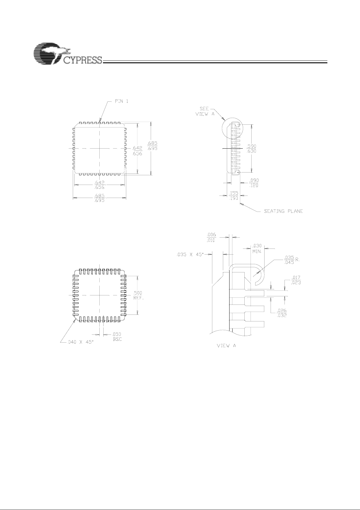
Ultra37000 CPLD Fami
ly
Document #: 38-03007 Rev. *B Page 49 of 63
Package Diagrams (continued)
44-Pin Ceramic Leaded Chip Carrier Y67
51-80014-**
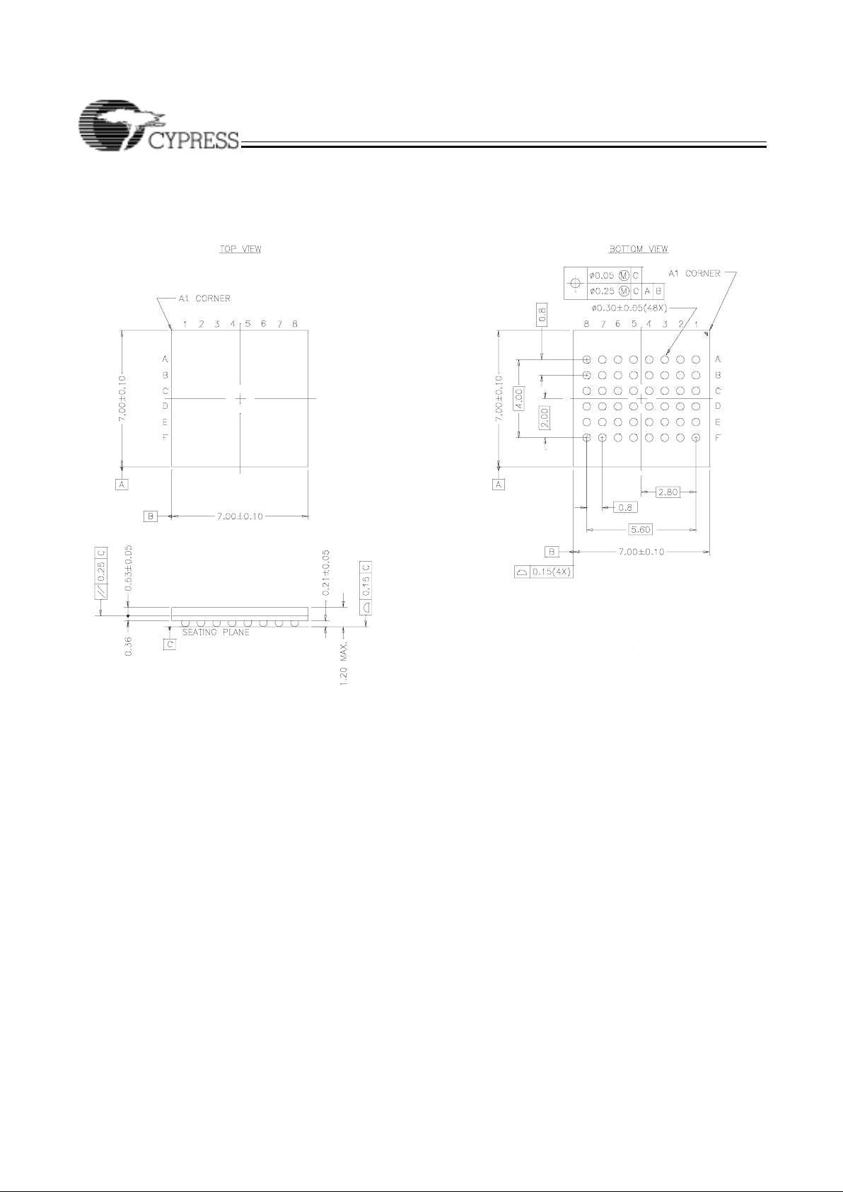
Ultra37000 CPLD Fami
ly
Document #: 38-03007 Rev. *B Page 50 of 63
Package Diagrams (continued)
48-Ball (7.0 mm x 7.0 mm x 1.2 mm, 0.80 pitch) Thin BGA BA48D
51-85109-*C
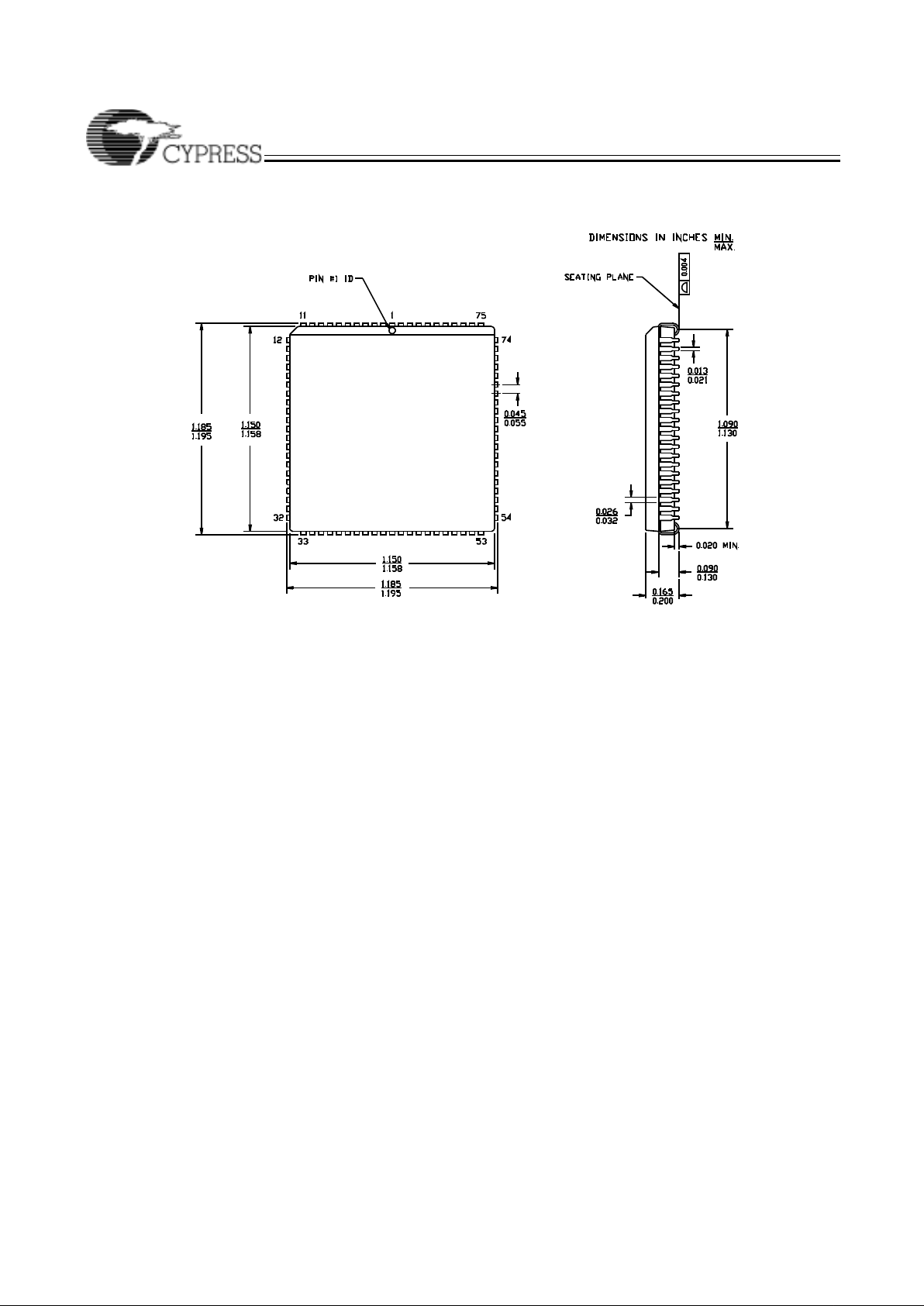
Ultra37000 CPLD Fami
ly
Document #: 38-03007 Rev. *B Page 51 of 63
Package Diagrams (continued)
84-Lead Plastic Leaded Chip Carrier J83
51-85006-*A
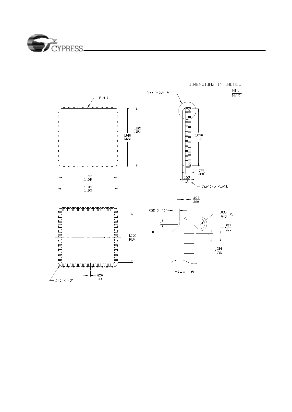
Ultra37000 CPLD Fami
ly
Document #: 38-03007 Rev. *B Page 52 of 63
Package Diagrams (continued)
84-Pin Ceramic Leaded Chip Carrier Y84
51-80095-*A
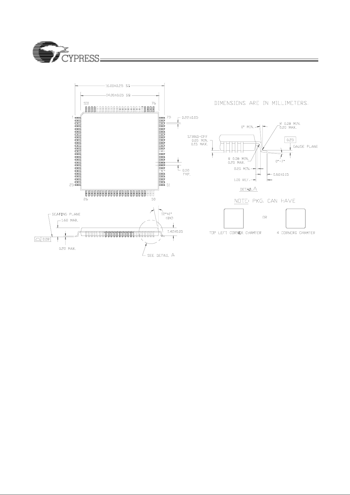
Ultra37000 CPLD Fami
ly
Document #: 38-03007 Rev. *B Page 53 of 63
Package Diagrams (continued)
100-Pin Thin Plastic Quad Flat Pack (TQFP) A100
51-85048-*B
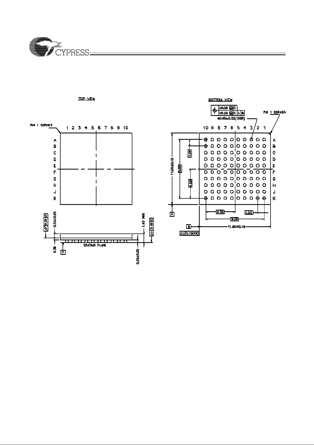
Ultra37000 CPLD Fami
ly
Document #: 38-03007 Rev. *B Page 54 of 63
Package Diagrams (continued)
100-Ba ll Thin Ball Grid Array (11 x 11 x 1.4 mm) BB100
51-8 510 7-*B
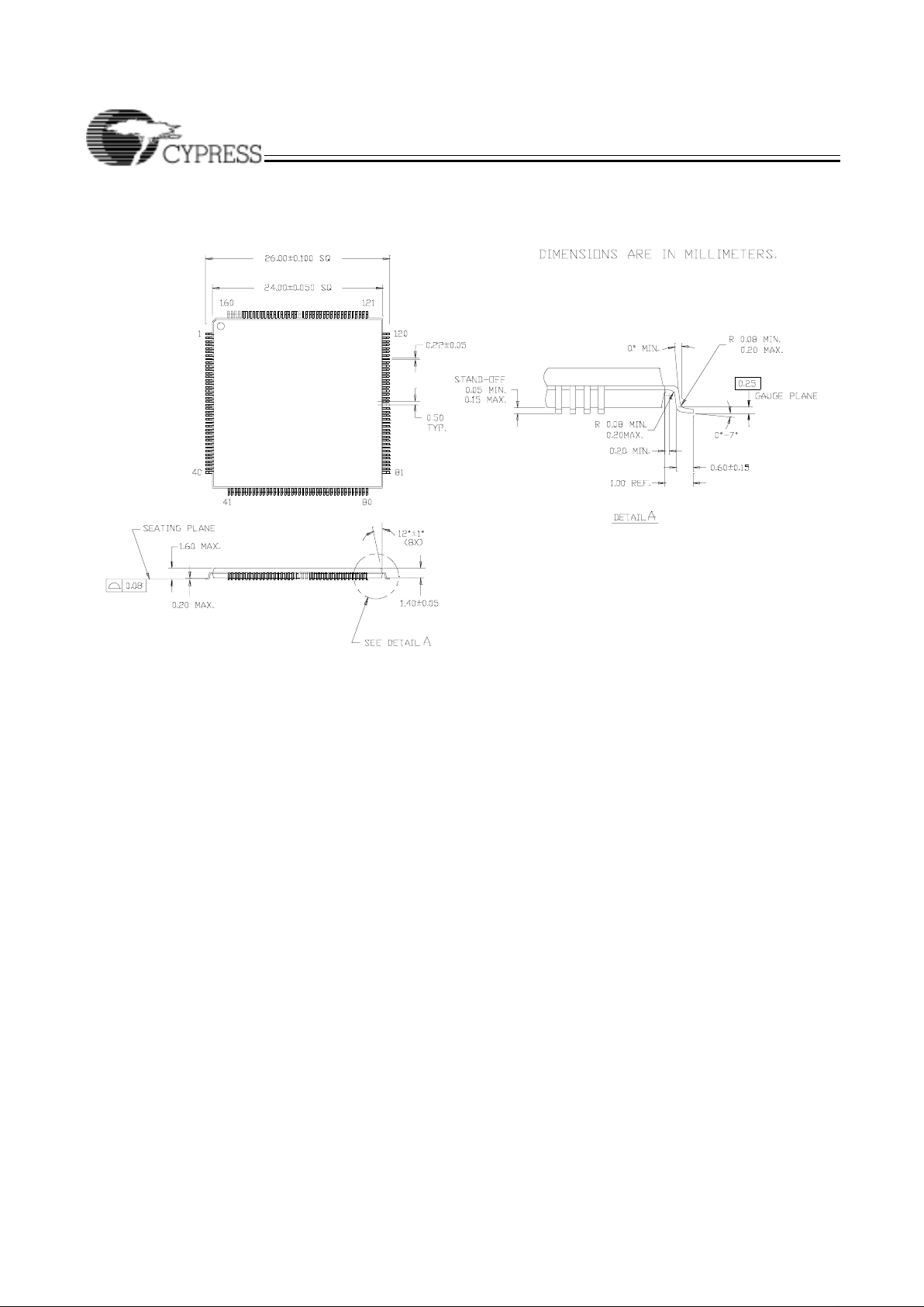
Ultra37000 CPLD Fami
ly
Document #: 38-03007 Rev. *B Page 55 of 63
Package Diagrams (continued)
160-Pin Thin Plastic Quad Flat Pack (24 x 24 x 1.4 mm) (TQFP) A160
51-85049-*B

Ultra37000 CPLD Fami
ly
Document #: 38-03007 Rev. *B Page 56 of 63
Package Diagrams (continued)
160-Lead Ceramic Quad Flatpack (Cavity Up) U162
51-80106-**

Ultra37000 CPLD Fami
ly
Document #: 38-03007 Rev. *B Page 57 of 63
Package Diagrams (continued)
208-Lead Plastic Quad Flatpack N208
51-85069-*B

Ultra37000 CPLD Fami
ly
Document #: 38-03007 Rev. *B Page 58 of 63
Package Diagrams (continued)
51-80105-*A
208-Lead Ceramic Quad Flatpack (Cavity Up) U208
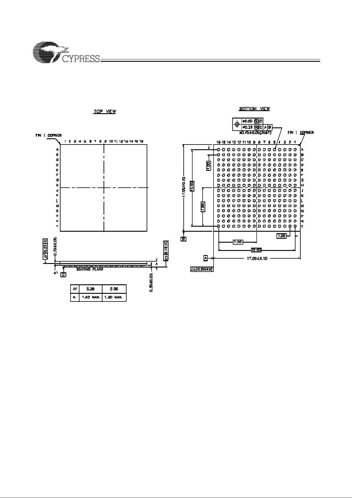
Ultra37000 CPLD Fami
ly
Document #: 38-03007 Rev. *B Page 59 of 63
Package Diagrams (continued)
256-Ball FBGA (17 x 17 mm) BB 256
51-85108-*C

Ultra37000 CPLD Fami
ly
Document #: 38-03007 Rev. *B Page 60 of 63
Package Diagrams (continued)
388-Lead PBGA (35 x 35 x 2. 33 mm) BG388
51-85103-*C

Ultra37000 CPLD Fami
ly
Document #: 38-03007 Rev. *B Page 61 of 63
Warp is a registered trademark, and In-Syst em Rep rogrammab le, ISR , Warp Profes sional, Warp Enterprise, and Ultra3 7000 are
trademarks, of C ypress Semic onducto r .V iewDraw a nd SpeedW av e are tra demarks of V iewLo gic. Wind ows is a reg istered tra demark of Microsoft Corporation. A ll product and company n ames mention ed in this do cument are the trademarks of the ir respective
holders.
Package Diagrams (continued)
400-Ball FBGA (21 x 21 x 1.4 mm) BB400
51-85111-*A

Ultra37000 CPLD Famil
y
Document #: 38-03007 Rev. *B Page 62 of 63
© Cypress Semiconductor Corporation, 2003. The information contained herein is subject to change without notice. Cypress Semiconductor Corporation assumes no responsibility for the use
of any circuitry other than cir cuitry embodied i n a Cypress Sem iconductor product . Nor does it convey or imply any license un der patent or other righ ts. Cypre ss Semiconductor does not autho rize
its products for use as critical components in life-support systems where a malfunction or failure may reasonably be expected to result in significant injury to the user. The inclusion of Cypress
Semiconductor products in life-support systems application implies that the manufacturer assumes all risk of such use and in doing so indemnifies Cypress Semiconductor against all charges.
Addendum
3.3V Operating Range
(CY37064VP100-143AC, CY37064VP100-143BBC, CY37064VP44-143AC, CY37064VP48-143BAC)
Range Ambient Temperature
[2]
Junction Temperature V
CC
Commercial 0°C to +70°C 0°C to +90°C 3.3V ± 0.16V

Ultra37000 CPLD Fami
ly
Document #: 38-03007 Rev. *B Page 63 of 63
Document History Page
Document Title: Ultra37000 CPLD Family 5V, 3.3V, ISR™ High-Performance CPLDs
Document Number: 38-03007
REV. ECN NO.
Issue
Date
Orig. of
Change Description of Change
** 106272 04/18/01 SZV Change from Spec number: 38-00475 to 38-03007
*A 124942 03/21/03 OOR Updated 3.3V V
cc
requirements for –144 speeds
Added an Addendum
*B 126262 05/09/03 TEH Changed pinout for CY37128V BB100 package
 Loading...