

Page 1
CY24272
Rambus® XDR™ Clock Generator with
Zero SDA Hold Time
Features
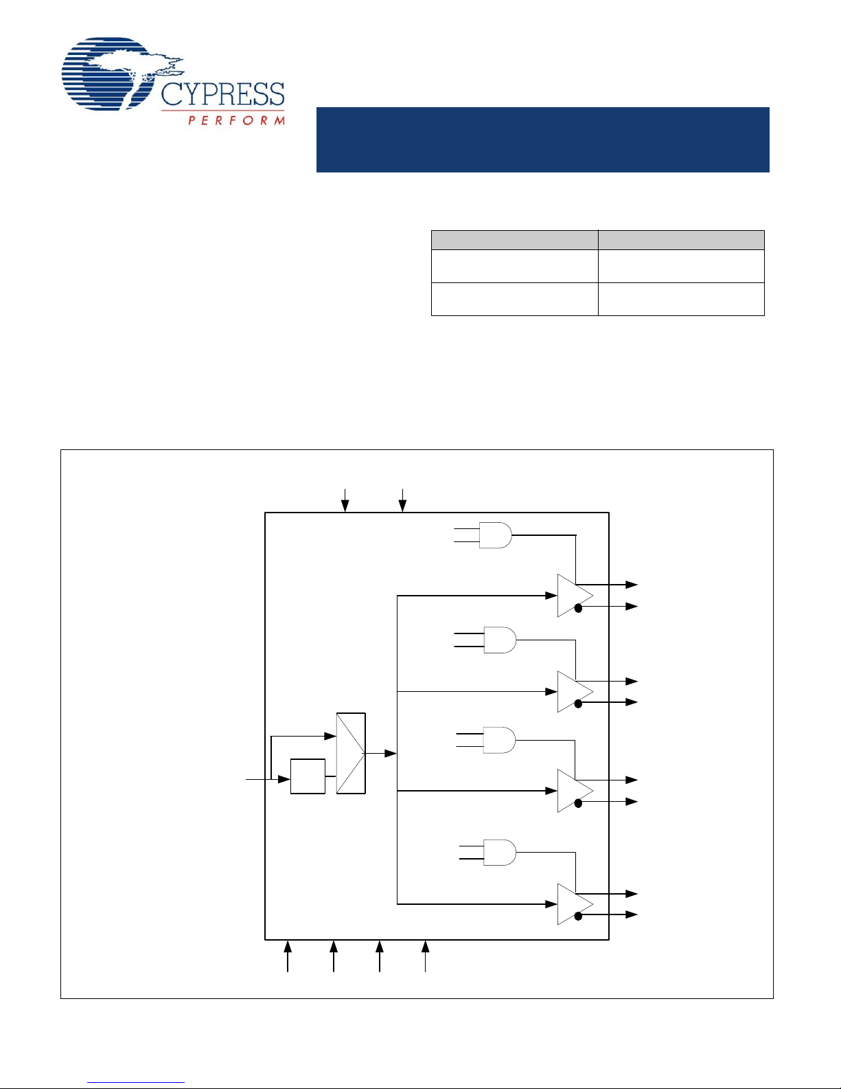
CLK0
CLK0B
CLK1
CLK1B
CLK2
CLK2B
CLK3
CLK3B
REFCLK,REFCLKB
SCL SDA ID0
ID1
EN
RegA
EN
RegB
EN
RegC
EN
RegD
PLL
Bypass
MUX
/BYPASS EN
Logic Block Diagram
■ Meets Rambus
requirements
■ 25 ps typical cycle-to-cycle jitter
❐ –135 dBc/Hz typical phase noise at 20 MHz offset
■ 100 or 133 MHz differential clock input
■ 300–667 MHz high speed clock support
■ Quad (open drain) differential output drivers
■ Supports frequency multipliers: 3, 4, 5, 6, 9/2 and 15/4
■ Spread Aware™
■ 2.5V operation
■ 28-pin TSSOP package
®
Extended Data Rate (XDR™) clocking
Table 1. Device Comparison
CY24271 CY24272
SDA hold time = 300 ns
(SMBus compliant)
R
= 200Ω typical
RC
(Rambus standard drive)
SDA hold time = 0 ns
2
(I
C compliant)
RRC = 295Ω minimum
(Reduced output drive)
Cypress Semiconductor Corporation • 198 Champion Court • San Jose, CA 95134-1709 • 408-943-2600
Document Number: 001-42414 Rev. ** Revised November 9, 2007
[+] Feedback
Page 2
CY24272
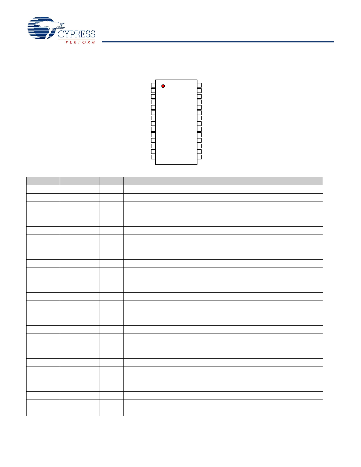
Pinouts
Figure 1. Pin Diagram - 28 Pin TSSOP
/BYPASS
REFCLKB
VDD
CLK0B
VSS
CLK2B
CLK3
CLK3B
VDD
VSS
CLK2
CLK0
VSS
CLK1
CLK1B
VDD
VDDP
ISET
VSSC
SDA
ID0
ID1
EN
SCL
VSSP
VSS
REFCLK
VDDC
1
2
3
4
5
6
7
8
9
10
11
12
13
14
28
27
26
25
24
23
22
21
20
19
18
17
16
15
CY24272
Table 2. Pin Definition - 28 Pin TSSOP
Pin No. Name IO Description
1 VDDP PWR 2.5V power supply for phased lock loop (PLL)
2 VSSP GND Ground
3 ISET I Set clock driver current (external resistor)
4 VSS GND Ground
5 REFCLK I Reference clock input (connect to clock source)
6 REFCLKB I Complement of reference clock (connect to clock source)
7 VDDC PWR 2.5V power supply for core
8 VSSC GND Ground
9 SCL I SMBus clock (connect to SMBus)
10 SDA I SMBus data (connect to SMBus)
1 1 EN I Output Enable (CMOS signal)
12 ID0 I Device ID (CMOS signal)
13 ID1 I Device ID (CMOS signal)
14 /BYPASS I REFCLK bypassing PLL (CMOS signal)
15 VDD PWR Power supply for outputs
16 CLK3B O Complement clock output
17 CLK3 O Clock output
18 VSS GND Ground
19 CLK2B O Complement clock output
20 CLK2 O Clock output
21 VSS GND Ground
22 VDD PWR Power supply for outputs
23 CLK1B O Complement clock output
24 CLK1 O Clock output
25 VSS GND Ground
26 CLK0B O Complement clock output
27 CLK0 O Clock output
28 VDD PWR Power supply for outputs
Document Number: 001-42414 Rev. ** Page 2 of 13
[+] Feedback
Page 3
CY24272
PLL Multiplier
Notes
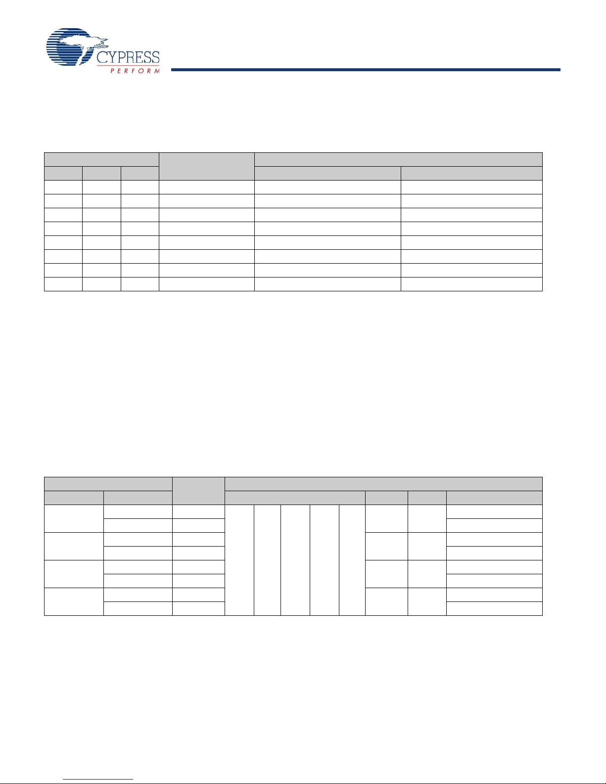
1. Output frequencies shown in Table 3 are based on nominal input frequencies of 100 MHz and 133.3 MHz. The PLL multipliers are applicable to spread spectrum
modulated input clock with maximum and minimum input cycle time. The REFSEL bit in SMBus 81h is set correctly as shown.
2. Default PLL multiplier at power up.
Table 3 shows the frequency multipliers in the PLL, selectable by programming the SMBus registers MULT0, MULT1, and MULT2.
Default multiplier at power up is 4.
Table 3. PLL Multiplier Selection
Register
MULT2 MULT1 MULT0 REFCLK = 100 MHz
Frequency Multiplier
Output Frequency (MHz)
[1]
, REFSEL = 0 REFCLK = 133 MHz
0 0 0 3 300 400
001 4 400
[2]
0 1 0 5 500 667
0 1 1 6 600 –
1 0 0 Reserved – –
1 0 1 9/2 450 600
1 1 0 Reserved – –
1 1 1 15/4 375 500
Input Clock Signal
The XCG receives either a differential (REFCLK/REFCLKB) or a
single-ended reference clocking input (REFCLK).
When the reference input clock is from a different clock source,
it must meet the voltage levels and timing requirements listed in
DC Operating Conditions on page 7 and AC Operating Conditions on page 8.
For a single-ended clock input, an external voltage divider and a
supply voltage, as shown in Figure 2 on page 6, provide a
reference voltage V
proper trip point of REFCLK. For the range of V
DC Operating Conditions on page 7, the outputs also meet the
at the REFCLKB pin. This determines the
TH
specified in
TH
Modes of Operation
The modes of operation are determined by the logic signals
applied to the EN and /BYPASS pins and the values in the five
SMBus Registers: RegTest, RegA, RegB, RegC, and RegD.
Table 5 on page 4 shows selection from one to all four of the
outputs, the Outputs Disabled Mode (EN = low), and Bypass
Mode (EN = high, /BYPASS = low). There is an option reserved
for vendor test. Disabled outputs are set to High Z.
At power up, the SMBus registers default to the last entry in Table
6 on page 5. The value at RegTest is 0. The values at RegA,
RegB, RegC, and RegD are all ‘1’. Thus, all outputs are
controlled by the logic applied to EN and /BYPASS.
DC and AC Operating Conditions tables.
[1]
, REFSEL = 1
–
Table 4. SMBus Device Addresses for CY24272
XCG
Device Operation Five Most Significant Bits ID1 ID0 WR# / RD
0
1
2
3
Document Number: 001-42414 Rev. ** Page 3 of 13
Write D8
Read D9 1
Write DA
Read DB 1
Write DC
Read DD 1
Write DE
Read DF 1
Hex
Address
11011
8-bit SMBus Device Address Including Operation
00
01
10
11
0
0
0
0
[+] Feedback
Page 4

CY24272
Notes
3. Bypass Mode: REFCLK bypasses the PLL to the output drivers.
4. Default mode of operation is at power up.
Table 5. Modes of Operation for CY24272
EN /BYPASS RegTest RegA RegB RegC RegD CLK0/CLK0B CLK1/CLK1B CLK2/CLK2B CLK3/CLK3B
L X X X X X X High Z High Z High Z High Z
H X 1 X X X X Reserved for Vendor Test
H L 0 X X X X REFCLK/
REFCLKB
[3]
REFCLK/
REFCLKB
REFCLK/
REFCLKB
REFCLK/
REFCLKB
H H 0 0 0 0 0 High Z High Z High Z High Z
H H 0 0 0 0 1 High Z High Z High Z CLK/CLKB
H H 0 0 0 1 0 High Z High Z CLK/CLKB High Z
H H 0 0 0 1 1 High Z High Z CLK/CLKB CLK/CLKB
H H 0 0 1 0 0 High Z CLK/CLKB High Z High Z
H H 0 0 1 0 1 High Z CLK/CLKB High Z CLK/CLKB
H H 0 0 1 1 0 High Z CLK/CLKB CLK/CLKB High Z
H H 0 0 1 1 1 High Z CLK/CLKB C LK/CLKB CLK/CLKB
H H 0 1 0 0 0 CLK/CLKB High Z High Z High Z
H H 0 1 0 0 1 CLK/CLKB High Z High Z CLK/CLKB
H H 0 1 0 1 0 CLK/CLKB High Z CLK/CLKB High Z
H H 0 1 0 1 1 CLK/CLKB High Z CLK/CLKB CLK/CLKB
H H 0 1 1 0 0 CLK/CLKB CLK/CLKB High Z High Z
H H 0 1 1 0 1 CLK/CLKB CLK/CLKB High Z CLK/CLKB
H H 0 1 1 1 0 CLK/CLKB CLK/CLKB CLK/CLKB High Z
HH 0
[4]
[4]
1
[4]
1
[4]
1
[4]
1
CLK/CLKB CLK/CLKB CLK/CLKB CLK/CLKB
Device ID and SMBus Device Address
The device ID (ID0 and ID1) is a part of the SMBus device 8-bit
address. The least significant bit of the address design ates a
write or read operation. Table 4 on page 3 shows the addresses
for four CY24272 devices on the same SMBus.
SMBus Protocol
The CY24272 is a slave receiver supporting operations in the
word and byte modes described in sections 5.5.4 and 5.5.5 of
the SMBus Specification 2.0.
DC specifications are modified to Rambus standard to support
1.8, 2.5, and 3.3 volt devices. Time out detection and packet
error protocol SMBus features are not supported.
Hold time for SDA is reduced relative to the CY24271, so that it
is compatible with I
2
C.
SMBus Data Byte Definitions
Three data bytes are defined for the CY24272. Byte 0 is for
programming the PLL multiplier registers and clock output
registers.
The definition of Byte 2 is sh own in Table 6, Table 7, and Table 8
on page 5. The upper five bits are the revision numbers of the
device and the lower three bits are the ID numbers assigned to
the vendor by Rambus.
Document Number: 001-42414 Rev. ** Page 4 of 13
[+] Feedback
Page 5

CY24272
Note
5. RW = Read and Write, RO = Read Only, POD = Power on default. See Table 3 on page 3 for PLL multipliers and Table 5 on page 4 for clock output selections.
Ta bl e 6. Command Code 80 h
[5]
Bit Register POD Type Description
7 Reserved 0 RW Reserved (no internal function)
6 MULT2 0 RW PLL Multiplier Select (reference Table 3 on page 3)
5MULT1 0 RW
4MULT0 1 RW
3 RegA 1 RW Clock 0 Output Select
2 RegB 1 RW Clock 1 Output Select
1 RegC 1 RW Clock 2 Output Select
0 RegD 1 RW Clock 3 Output Select
Ta bl e 7. Command Code 81 h
[5]
Bit Register POD Type Description
7 Reserved 0 RW Reserved (no internal function)
6 Reserved 0 RW
5 Reserved 0 RW
4 Reserved 0 RW
3 Reserved 1 RW Reserved (must be set to ‘1’ for proper operation)
2 REFSEL 0 RW Reference Frequency Select (reference Table 3 on page 3)
1 Reserved 0 RW Reserved (must be set to ‘0’ for proper operation)
0 RegTest 0 RW Reserved (must be set to ‘0’ for proper operation)
Ta bl e 8. Command Code 82 h
[5]
Bit Register POD Type Description
7Device
6?RO
5?RO
Revision
Number
? RO Contact factory for Device Revision Number information.
4?RO
3?RO
2 Vendor ID 0 RO Rambus assigned Vendor ID Code
11RO
00RO
Document Number: 001-42414 Rev. ** Page 5 of 13
[+] Feedback
Page 6

CY24272
Figure 2. Differential and Single-Ended Clock Inputs
REFCLKB
REFCLK
Input
XDR Clock Generator
Inpu t
XDR Clock Generator
REFCLK
Supply Voltage
V
TH
Differential Input Single-ended Input
Absolute Maximum Conditions
Parameter Description Condition Min Max Unit
V
DD
V
DDC
V
DDP
V
IN
T
S
T
A
T
J
Ø
JA
ESD
HBM
Clock Buffer Supply Voltage –0.5 4.6 V
Core Supply Voltage –0.5 4.6 V
PLL Supply Voltage –0.5 4.6 V
Input Voltage (SCL and SDA) Relative to V
Input Voltage (REFCLK/REFCLKB
) Relative to V
Input Voltage Relative to V
SS
SS
SS
–0.5 4.6 V
–0.5 V
–0.5 V
+ 1.0 V
DD
+ 0.5 V
DD
Temperature, Storage Non-functional –65 150 °C
Temperature, Op erating Ambient Functional 0 70 °C
Temperature, Junction Functional – 150 °C
Junction to Ambient thermal resis-
Zero air flow – 100 °C/W
tance
ESD Protection (Human Body Model) MIL-STD-883, Method 3015 2000 – V
Document Number: 001-42414 Rev. ** Page 6 of 13
[+] Feedback
Page 7

CY24272
DC Operating Conditions
Notes
6. Not 100% tested except V
IXCLK
and ΔV
IXCLK
. Parameters guaranteed by design and characterizations, not 100% tested in production.
7. This range of SCL and SDA input high voltage enables the CY24272 for use with 3.3V, 2.5V, or 1.8V SMBus voltages.
8. Single-ended operation guaranteed only when 0.8 < (V
IH,SE
– VTH)/(V
TH
– VIL,SE) < 1.2.
Parameter Description Condition Min Max Unit
V
DDP
V
DDC
V
DD
V
IHCLK
V
ILCLK
V
IXCLK
ΔV
V
IH
V
IL
V
IH,SM
V
IL,SM
V
TH
V
IH,SE
V
IL,SE
T
A
IXCLK
[8]
Supply Voltage for PLL 2.5V ± 5% 2.375 2.625 V
Supply Voltage for Core 2.5V ± 5% 2.375 2.625 V
Supply Voltage for Clock Buffers 2.5V ± 5% 2.375 2.625 V
Input High Voltage, REFCLK/REFCLKB 0.6 0.95 V
Input Low Voltage, REFCLK/REFCLKB –0.15 +0.15 V
[6]
Crossing Point Voltage, REFCLK/REFCLKB 200 550 mV
[6]
Difference in Crossing Point Voltage, REFCLK/REFCLKB – 150 mV
Input Signal High Voltage at ID0, ID1, EN, and /BYPASS 1.4 2.625 V
Input Signal Low Voltage at ID0, ID1, EN, and /BYPASS –0.15 0.8 V
Input Signal High Voltage at SCL and SDA
[7]
1.4 3.465 V
Input Signal Low Voltage at SCL and SDA –0.15 0.8 V
Input Threshold Voltage for single-ended REFCLK 0.35 0.5V
Input Signal High Voltage for single-ended REFCLK V
+ 0.3 2.625 V
TH
Input Signal Low Voltage for single-ended REFCLK –0.15 VTH – 0.3 V
Ambient Operating Temperature 0 70 °C
DD
V
Document Number: 001-42414 Rev. ** Page 7 of 13
[+] Feedback
Page 8

CY24272
AC Operating Conditions
Notes
9. Jitter measured at crossing points and is the absolute value of the worst case deviati on.
10.Measured at crossing points.
11.If input modulation is used; input modulation is allowed but not required.
12.The amount of allowed spreading for any non-triangular modulation is det ermined by the induced downstr eam tracking skew t hat cannot exceed the skew generated
by the specified 0.6% triangular modulation. Typically , the amount of allowed non-triangular modulation is about 0.5%.
13.V
OX
is measured on external divider network.
14.V
COS
= (clock output high voltage – clock output low voltage), measured on the external divider network.
15.V
OL_ABS
is measured at the clock output pins of the package.
16.I
REF
is equal to V
ISET/RRC
.
17.Min im um I
OL,ABS
is measured at the clock output pin with RRC = 266 ohms or less.
18.Z
OUT
is defined at the output pins as (0.94V – 0.90V)/(I
0.94
– I
0.90
) under conditions specified for I
OL, ABS
.
The AC operating conditions follow.
Parameter Description Condition Min Max Unit
t
CYCLE,IN
t
JIT,IN(cc)
[10]
t
DCIN
t
/ t
RIN
Δt
/ t
RIN
[11]
p
MIN
FIN
REFCLK, REFCLKB input cycle time REFSEL = 0, /BYPASS = High 9 11 ns
Input Cycle to Cycle Jitter
Input Duty Cycle Over 10,000 cycles 40% 60% t
Rise and Fall Times Measured at 20%–80% of input
Rise and Fall Times Difference – 150 ps
FIN
Modulation Index for triangular modulation – 0.6 %
Modulation Index for non-triangular modulation – 0.5
[11]
f
MIN
t
SR,IN
C
IN,REF
C
IN,CMOS
f
SCL
Input Frequency Modulation 30 33 kHz
Input Slew Rate (measured at 20%–80% of
input voltage) for REFCLK
Capacitance at REFCLK inputs – 7 pF
Capacitance at CMOS inputs – 10 pF
SMBus clock frequency input in SCL pin DC 100 kHz
[6]
REFSEL = 1, /BYPASS = High 7 8 ns
/BYPASS = Low 4 – ns
[9]
–185ps
175 700 ps
voltage for REFCLK and
REFCLKB inputs
[12]
14V/ns
CYCLE
%
DC Electrical Specifications
Parameter Description Min Typ Max Unit
[6]
V
OX
V
COS
V
OL,ABS
V
ISET
[7]
I
DD
[7]
I
DD
I
OL/IREF
I
OL,ABS
V
OL,SDA
I
OL,SDA
I
OZ
Z
OUT
Differential output crossing point voltage
[6]
Output voltage swing (peak-to-peak single-ended)
Absolute output low voltage at CLK[3:0], CLK[3:0]B
Reference voltage for swing controlled current, I
Power Supply Current at 2.625V, f
Power Supply Current at 2.625V, f
Ratio of output low current to reference current
Minimum current at V
OL,ABS
[17]
SDA output low voltage at test condition of SDA output low current = 4 mA – – 0.4 V
SDA output low voltage at test condition of SDA voltage = 0.8V 6 – – mA
Current during High Z per pin at CLK[3:0], CLK[3:0]B – – 10 μA
Output dynamic impedance when clock output signal is at VOL = 0.9V
[13]
= 100 MHz, and f
ref
= 133 MHz, and f
ref
[16]
–1.08–V
[14]
[15]
0.98 1.0 1.02 V
REF
= 300 MHz – – 85 mA
out
= 667 MHz – – 125 mA
out
–400–mV
0.85 – – V
6.8 7.0 7.2
25 – – mA
[18]
1000 – – Ω
Document Number: 001-42414 Rev. ** Page 8 of 13
[+] Feedback
Page 9

CY24272
AC Electrical Specification
The AC Electrical specifications follow.
Parameter Description Min Typ Max Unit
t
CYCLE
t
JIT(cc)
Clock Cycle time
Jitter over 1-6 clock cycles at 400–635 MHz
[19]
Jitter over 1-6 clock cycles at 638–667 MHz – 25 30 ps
L
20
Phase noise SSB spectral purity L(f) at 20 MHz offset: 400–500 MHz
(In addition, device must not exceed L(f) = 10log[1+(50x10
f = 1 MHz to 100 MHz except for the region near f = REFCLK/Q where Q is
the value of the internal reference divider.)
t
JIT(hper,cc)
Cycle-to-cycle duty cycle error at 400–635 MHz – 25 40 ps
Cycle-to-cycle duty cycle error at 636–667 MHz – 25 30 ps
Δt
SKEW
Drift in t
supply voltage varies between 2.375V and 2.625V.
when ambient temperature varies between 0°C and 70°C and
SKEW
DC Long term average output duty cycle 45% 50 55% t
t
EER,SCC
tCR,t
CF
t
CR,CF
PLL output phase error when tracking SSC –100 – 100 ps
Output rise and fall times at 400–667 MHz (measured at 20%–80% of output
voltage)
Difference between output rise and fall times on the same pin of the single
device (20%–80%) of 400–667 MHz
Table 9. SMBus Timing Specification
Parameter Description Min Max Units
FSMB SMBus Operating Frequency 10 100 kHz
TBUF Bus free time between Stop and Start Condition 4.7 μs
THD:ST A Hold time after (Repeated) Start Condition.
After this period, the first clock is generated.
TSU:STA Repeated Start Condition setup time 4.7 μs
TSU:STO Stop Condition setup time 4.0 μs
THD:DAT Data Hold time 0 ns
TSU:DAT Data Setup time 250 ns
TTIMEOUT Detect clock low timeout Not supported
TLOW Clock low period 4.7 μs
THIGH Clock high period 4.0 50 μs
TLOW:SEXT Cumulative clock low extend time (slave device) 25 ms
TLOW:MEXT Cumulative clock low extend time (master device) 10 ms
TF Clock/Data Fall Time 300 ns
TR Clock/Data Rise Time 1000 ns
TPOR Time in which a device must be operational after power on reset 500 ms
[6]
1.25 3.34 ns
[20]
[21]
6
/f)
2.4
] –138 for
–2540ps
– –135 –128 dBC/Hz
––15ps
CYCLE
–150–ps
[22]
– – 100 ps
4.0 μs
CY24272 doesn’t
extend
Document Number: 001-42414 Rev. ** Page 9 of 13
[+] Feedback
Page 10

CY24272
Test and Measurement Setup
Differential Driver
CLK
CLKB
Swing Curre n t
Control
ISET
R
RC
Measureme nt
Point
V
TS
R
1
Z
CH
V
T
R
T1
C
S
R
T2
R
3
R
2
Measureme nt
Point
V
TS
R
1
Z
CH
V
T
R
T1
C
S
R
T2
R
3
R
2
Notes
19.Max and min output clock cycle times are based on nominal outputs frequency of 300 and 667 MHz, respectively. For spread spectrum modulated differential or
single-ended REFCLK, the output clock tracks the modulation of the input.
20.Output short term jitter spec is the absolute value of the worst case deviation.
21.t
SKEW
is the timing difference between any two of the four differential clocks and is measured at common mode voltage. Δt
SKEW
is the change in t
SKEW
when the
operating temperature and supply voltage change.
22.t
CR,CF
applies only when appropriate RRC and output resistor network resistor values are selected to match pull up and pull down currents.
Figure 3. Clock Outputs
Example External Resistor Values
and Termination Voltages for a 50Ω Channel
Parameter Value Unit
R
1
R
2
R
3
R
T1
R
T2
C
S
R
RC
V
TS
V
T
33.0 Ω
18.0 Ω
17.0 Ω
60.4 Ω
301 Ω
2700 pF
432 Ω
2.5V V
1.2V V
Signal Waveforms
A physical signal that appears at the pins of a device is deemed
valid or invalid depending on its voltage and timing relations with
other signals. Input and output voltage waveforms are defined as
shown in Figure 4 on page 11. Both rise and fall times are defined
between the 20% and 80% points of the voltage swing, with the
swing defined as V
H–VL
.
Figure 5 on page 11 shows the definition of the output crossing
point. The nominal crossing point between the complementary
outputs is defined as the 50% point of the DC voltage levels.
There are two crossing points defined: Vx+ at the rising edge of
CLK and Vx– at the falling edge of CLK. For some waveforms,
both Vx+ and Vx– are below Vx,nom (for example, if t
CF
).
than t
is larger
CR
Jitter
This section defines the specifications that relate to timing uncertainty (or jitter) of the input and output waveforms. Figure 6 on
page 11 shows the definition of cycle-to-cycle jitter with re spect
to the falling edge of the CLK signal. Cycle-to-cycle jitter is the
difference between cycle times of adjacent cycles. Equal requirements apply rising edges of the CLK signal. Figure 7 on page 11
shows the definition of cycle-to-cycle duty cycle error (t
Cycle-to-cycle duty cycle is defined as the difference between
t
(high times) of adjacent differential clock cycles. Equal
PW+
requirements apply to t
cycles.
, low times of the differential click
PW-
DC,ERR
).
Document Number: 001-42414 Rev. ** Page 10 of 13
[+] Feedback
Page 11

CY24272
Figure 4. Input and Output Waveforms
V
H
t
R
t
F
80%
20%
V
L
V
(t)
Vx.nom
CLK
CLKB
Vx+
Vx-
CLK
CLKB
t
CYCLE,i
t
CYCLE,i+1
tJ = t
CYCLE,i
- t
CYCLE,i+1 over 10,000 consecutive cycles
CLK
CLKB
t
CYCLE,
(i)
t
PW-
(i)
t
PW+
(i)
t
PW-
(i+1)
t
PW+
(i+1)
t
CYCLE,
(i+1)
t
DC,ERR
= t
PW-
(i) - t
PW-
(i+1) and t
PW-
(i+1) - t
PW+
(i+1)
Figure 5. Crossing Point Voltage
Figure 6. Cycle-to-cycle Jitter
Document Number: 001-42414 Rev. ** Page 11 of 13
Figure 7. Cycle-to-cycle Duty-cycle Error
[+] Feedback
Page 12

CY24272
Ordering Information
PIN 1 ID
SEATING
PLANE
BSC.
BSC
0°-8°
PLANE
GAUGE
1
28
9.60[0.378]
1.10[0.043] MAX.
0.65[0.025]
0.20[0.008]
0.05[0.002]
6.50[0.256]
0.076[0.003]
6.25[0.246]
4.50[0.177]
4.30[0.169]
9.80[0.386]
0.15[0.006]
0.19[0.007]
0.30[0.012]
0.09[[0.003]
0.25[0.010]
0.70[0.027]
0.50[0.020]
0.95[0.037]
0.85[0.033]
51-85120-*A
Part Number Package Type Product Flow
Pb-Free
CY24272ZXC 28-pin TSSOP Commercial, 0°C to 70°C
CY24272ZXCT 28-pin TSSOP – Tape and Reel Commercial, 0°C to 70°C
Package Drawing and Dimension
Figure 8. 28-Pin Thin Shrunk Small Outline Package (4.40-mm Body) ZZ28
Document Number: 001-42414 Rev. ** Page 12 of 13
[+] Feedback
Page 13

CY24272
Document History Page
Document Title: CY24272 Rambus® XDR™ Clock Generator with Zero SDA Hold Time
Document Number: 001-42414
REV. ECN NO.
Issue
Date
** 1749003 See ECN KVM/AESA New data sheet
Orig. of
Change
Description of Change
No 8 or 15/2 multipliers or 133MHz * 4 option
Max frequency is 667MHz
© Cypress Semiconductor Corporation, 2007. The information contained herein is subject to change without notice. Cypress Semiconductor Corporation assumes no responsibility for the use of any
circuitry other than circuitry embodied in a Cypress product. Nor does it convey or imply any license under patent or other rights. Cypress products are not warranted nor int ended to be used for med ical,
life support, life saving, critical control or safety applications, unless pursuant to an express written agreement with Cypress. Furthermore, Cypress does no t author ize its products fo r use as critica l
components in life-support systems where a malfunction or failure may reasonably be expected to result in significant injury to the user. The inclusion of Cypress products in life-support systems
application implies that the manufacturer assumes all risk of such use and in doing so indemnifies Cypress against all charges.
Any Source Code (software and/or firmware) is owned by Cypress Semiconductor Corporation (Cypress) and is protected by and subject to worldwide patent protection (United States and foreign),
United States copyright laws and international treaty provisions. Cypress hereby gr ant s to l icense e a pers onal, no n-exclu sive , non-tr ansfer able license to copy, use, modify, create derivative works of,
and compile the Cypress Source Code and derivative works for the sole purpose of creating custom software and or firmware in support of licensee product to be used only in conju nction with a Cypress
integrated circuit as specified in the ap plicable agreem ent. Any reprod uction, modificatio n, translation, co mpilation, or repr esentation of this Source Co de except as speci fied above is pro hibited with out
the express written permission of Cypress.
Disclaimer: CYPRESS MAKES NO WARRANTY OF ANY KIND, EXPRESS OR IMPLIED, WITH REGARD TO THIS MATERIAL, INCLUDING, BUT NOT LIMITED TO, THE IMPLIED WARRANTIES
OF MERCHANTABILITY AND FITNESS FOR A PARTICULAR PURPOSE. Cypress reserves the right to make changes without further notice to the materials described herein. Cypress doe s not
assume any liability arising out of the applic ation or use o f any pr oduct or circ uit de scribed herein . Cypr ess does n ot author ize its p roducts fo r use as critical compon ents in life-su pport systems whe re
a malfunction or failure may reason ably be expected to result in significant injury to the user. The inclusion of Cypress’ product in a life-support systems application implies that the manufacturer
assumes all risk of such use and in doing so indemnifies Cypress against all charges.
Use may be limited by and subject to the applicable Cypress software license agreement.
Document Number: 001-42414 Rev. ** Revised November 9, 2007 Page 13 of 13
PSoC Designer™, Programmable System-on-Chip™, and PSoC Express™ are trademarks and PSoC® is a registered t rade mark of Cypress S em ic on duct or C orp. A ll other trademarks or registered
trademarks referenced he rein are property of the re spective c orporatio ns. Purch ase of I2C components from Cypress or one of its sublicensed Associated Companies conveys a license under the
Philips I2C Patent Rights to use these components in an I2C system, provided that the system conforms to the I2C Standard Specification as defined by Philips. S pread Aware is a trademark of Cypress
Semiconductor Corporation. Ramb us is a r egistere d tradema rk, and X DR i s a trade mark, of R ambus In c. All products and comp any name s mentio ned in this do cument may be the tr ademarks o f their
respective holders.
[+] Feedback
 Loading...