

Cypress Semiconductor CY2309SC-1T, CY2309SC-1H, CY2309SC-1, CY2309ZI-1HT, CY2309ZI-1H Datasheet
...
CY2305
CY2309
Low-cost 3.3V Zero Delay Buffer
Features
• 10-MHz to 100-/133-MHz operating range, compatible
with CPU and PCI bus frequencies
• Zero input-output propagation delay
• Multiple low-skew outputs
—Output-output skew less than 250 ps
—Device-device skew less than 700 ps
—One input drives five outputs (CY2305)
—One input drives nine outputs, group ed as 4 + 4 + 1
(CY2309)
• Less than 200 ps cycle-cycle jitter, compatible with
Pentium
-based systems
• Te st Mode to bypass phase-locked loop (PLL) (CY2309
only [see “Select Input Decoding” on page 2])
• Available in sp ac e-sa vin g 16-pin 150 -mil SOIC or
4.4-mm TSSOP p ack age s (CY2 309 ), a nd 8-pin , 1 50-m il
SOIC package (CY2305)
• 3.3V operation
• Industrial temperature available
Functional Description
The CY2309 is a low-cost 3.3V zero delay buffer designed to
distribute high-speed clocks and is avail able in a 16-p in SOIC
or TSSOP package. The CY2305 is an 8-pin version of the
CY2309. It accepts one reference input, and drives out five
low-skew clocks. The -1H versions of each device operate at
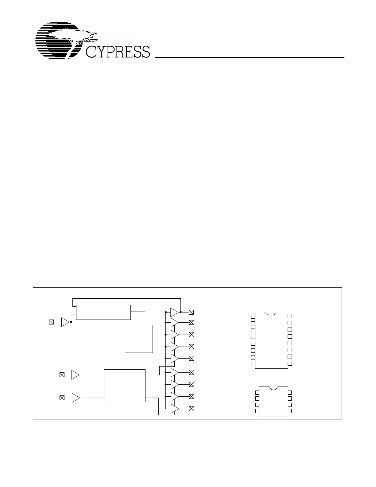
Block Diagram
PLL
REF
S2
Select Input
Decoding
S1
2309-1
MUX
up to 100-/133-MHz frequencies, and have higher drive than
the -1 devices. All parts have on-chip PLLs which lock to an
input clock on the REF pin. The PLL feedback is on-chip and
is obtained from the CLKOUT pad.
The CY2309 has two banks of four outputs each, which can
be controlled by the Sele ct inputs as shown in the “Select Input
Decoding” table on page 2. If all outp ut clocks are not required,
BankB can be three-stated. The select inputs also allow the
input clock to be directly app lied to the out puts for chip and
system testing purposes.
The CY2305 and CY2309 PLLs enter a power-down mode
when there are no rising ed ges on the R EF input. In this state,
the outputs are three-s tated and the PLL is turned of f, resulting
in less than 12.0 µA of current draw for commercial temperature devices and 25.0 µA for indus trial temperature p arts. The
CY2309 PLL shuts down in one additional case as shown in
the table below.
Multiple CY2305 and CY2309 devices can accept the same
input clock and di stribute it. In this case, the skew betwe en the
outputs of two devices is guaranteed to be less than 700 ps.
All outputs ha ve less than 20 0 ps of cycl e-cycle jitter . The input
to output propagation delay on both devices is guaranteed to
be less than 350 ps, and the output to output skew is
guaranteed to be less than 250 ps.
The CY2305/CY2309 is avai lable in two/thre e diff erent conf igurations, as shown in the ordering information (page 10). The
CY2305-1/CY2309-1 is the base part. The CY2305-1H/
CY2309-1H is the high-dri ve ve rsion of the - 1, and i ts rise a nd
fall times are much faster than the -1s.
Pin Configuration
SOIC/TSSOP
DD
S2
REF
CLK2
CLK1
GND
Top View
1
2
3
4
5
6
7
8
SOIC
Top View
1
2
3
4
16
15
14
13
12
11
10
9
8
7
6
5
CLKOUT
CLKA4
CLKA3
V
DD
GND
CLKB4
CLKB3
S1
CLKOUT
CLK4
V
DD
CLK3
2309-2
2309-3
CLKOUT
CLKA1
CLKA2
CLKA3
CLKA4
CLKB1
CLKB2
CLKB3
CLKB4
REF
CLKA1
CLKA2
V
GND
CLKB1
CLKB2
Cypress Semiconductor Corporation • 3901 North First Street • San Jose, CA 95134 • 408-943-2600
Document #: 38-07140 Rev. *C Revised December 14, 2002
Pin Description for CY2309
Pin Signal Description
DD
[1]
Input reference frequency, 5V-tolerant inp ut
[2]
[2]
Buffered clock output, Bank A
Buffered clock output, Bank A
3.3V supply
1REF
2 CLKA1
3 CLKA2
4V
5 GND Ground
6 CLKB1
7 CLKB2
8S2
9S1
10 CLKB3
1 1 CLKB4
[2]
[2]
[3]
[3]
[2]
[2]
Buffered clock output, Bank B
Buffered clock output, Bank B
Select input, bit 2
Select input, bit 1
Buffered clock output, Bank B
Buffered clock output, Bank B
12 GND Ground
13 V
14 CLKA3
15 CLKA4
DD
[2]
[2]
16 CLKOUT
[2]
3.3V supply
Buffered clock output, Bank A
Buffered clock output, Bank A
Buffered output, interna l feed bac k on this pin
CY2305
CY2309
Pin Description for CY2305
Pin Signal Description
1REF
2CLK2
3CLK1
[1]
[2]
[2]
Input reference frequency, 5V-tolerant inp ut
Buffered clock output
Buffered clock output
4 GND Ground
DD
[2]
[2]
[2]
Buffered clock output
3.3V supply
Buffered clock output
Buffered clock output, internal feedback on this pin
5CLK3
6V
7CLK4
8 CLKOUT
Select Input Decoding for CY2309
S2 S1 CLOCK A1–A4 CLOCK B1–B4 CLKOUT
0 0 Three-state Three-state Driven PLL N
0 1 Driven Three-state Driven PLL N
1 0 Driven Driven Driven Reference Y
1 1 Driven Driven Driven PLL N
Notes:
1. Weak pull-down.
2. Weak pull-down on all outputs.
3. Weak pull -ups on these inputs.
4. This output is driven and has an internal feedback for the PLL. The load on this output can be adjusted to change the skew between the reference and output.
[4]
Output Source PLL Shutdown
Document #: 38-07140 Rev. *C Page 2 of 13
CY2305
CY2309
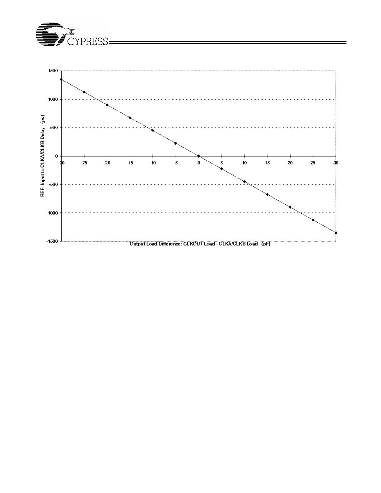
REF. Input to CLKA/CLKB Delay vs. Loading Difference between CLKOUT and CLKA/CLKB Pins
Zero Delay and Skew Control
All outputs should be uniformly loaded to achieve Zero Delay
between the input and output. Since the CLKOUT pin is the
internal feedback to the PLL , its relativ e loading can adj ust the
input-output delay. This is shown in the above graph.
For applications requiring zero input-output delay, all outputs,
including CLKOUT, must be equally loaded. Even if CLKOUT
is not used, it must have a capacitive load, equal to that on
other outputs, for obtaining zero input-output delay. If input to
output delay adjustmen ts are required, use the above graph to
calculate lo ading differences between the CLKOUT pin and
other outputs.
For zero output-output skew, be sure to load all outputs
equally. For further information refer to the application note
entitled “CY2305 and CY2309 as PCI and SDRAM Buffers.”
Document #: 38-07140 Rev. *C Page 3 of 13
Maximum Ratings
CY2305
CY2309
Supply Voltage to Ground Potential...............–0.5V to +7.0V
DC Input Voltage (Except REF) ............–0.5V to VDD + 0.5V
DC Input Voltage REF.........................................–0.5V to 7V
Storage Temperature .................................–65°C to +150°C
Junction Temperature................................................. 150°C
Static Discharge Voltage
(per MIL-STD-883, Method 3015) ...........................> 2,000V
Operating Conditions for CY2305SC-XX and CY2309SC-XX Commercial Temperature Devices
Parameter Description Min. Max. Unit
V
DD
T
A
C
L
C
L
C
IN
Supply Voltage 3.0 3.6 V
Operating Temperature (Ambient Temperature) 0 70 °C
Load Capacitance, below 100 MHz 30 pF
Load Capacitance, from 100 MHz to 133 MHz 10 pF
Input Capacitance 7 pF
Power-up time for all VDD's to reach minimum specified voltage
t
PU
(power ramps must be monotonic) 0.05 50 ms
Electrical Characteristics for CY2305SC-XX and CY2309SC-XX Commercial Temperature Devices
Parameter Description Test Conditions Min. Max. Unit
[6]
DD
[5]
[5]
= 0V 50.0 µA
IN
[6]
[6]
DD
IOL = 8 mA (–1)
I
12 mA (–1H)
OH =
IOH = –8 mA (–1)
I
= –12 mA (–1H)
OL
2.0 V
2.4 V
0.8 V
100.0 µA
0.4 V
32.0 mA
SEL inputs at V
10-pF load
1
Measured at 1.4V, F
DD
10
10
= 66.67 MHz 40.0 50.0 60.0 %
out
100
133.33
[7]
MHz
MHz
Measured between 0.8V and 2.0V 2.50 ns
Measured between 0.8V and 2.0V 2.50 ns
[6]
All outputs equally loaded 250 ps
Measured at VDD/2 0 ±350 ps
[6]
Measured at VDD/2. Measured in PLL
[6]
Bypass Mode, CY2309 device only.
[6]
Measured at VDD/2 on the CLKOUT pins
158.7ns
0700ps
of devices
Measured at 66 .67 MHz, load ed outp uts 200 ps
Stable power supply, valid clock
1.0 ms
presented on REF pin
/2.
V
IL
V
IH
I
IL
I
IH
V
OL
V
OH
(PD mode) Power Down Supply Current REF = 0 MHz 12.0 µA
I
DD
I
DD
Input LOW Voltage
Input HIGH Voltage
Input LOW Current V
Input HIGH Current VIN = V
Output LOW Voltage
Output HIGH Voltage
Supply Current Unloaded outputs at 66.67 MHz,
Switching Characteristics for CY2305SC-1and CY2309SC-1 Commercial Temperature Devices
Parameter Name Test Conditions Min. Typ. Max. Unit
t1 Output Frequency 30-pF load
[6]
Duty Cycle
t3 Rise Time
t
4
t
5
t
6A
t
6B
t
7
t
J
t
LOCK
Notes:
5. REF input has a threshold voltage of V
6. Parameter is guaranteed by design and characterization. Not 100% tested in production.
7. All parameters specified with loaded outputs.
Fall Time
Output to Output Skew
Delay, REF Rising Edge to
CLKOUT Rising Edge
Delay, REF Rising Edge to
CLKOUT Rising Edge
Device to Device Skew
Cycle to Cycle Jitter
PLL Lock Time
= t2 ÷ t
[6]
[6]
[6]
Document #: 38-07140 Rev. *C Page 4 of 13
 Loading...