

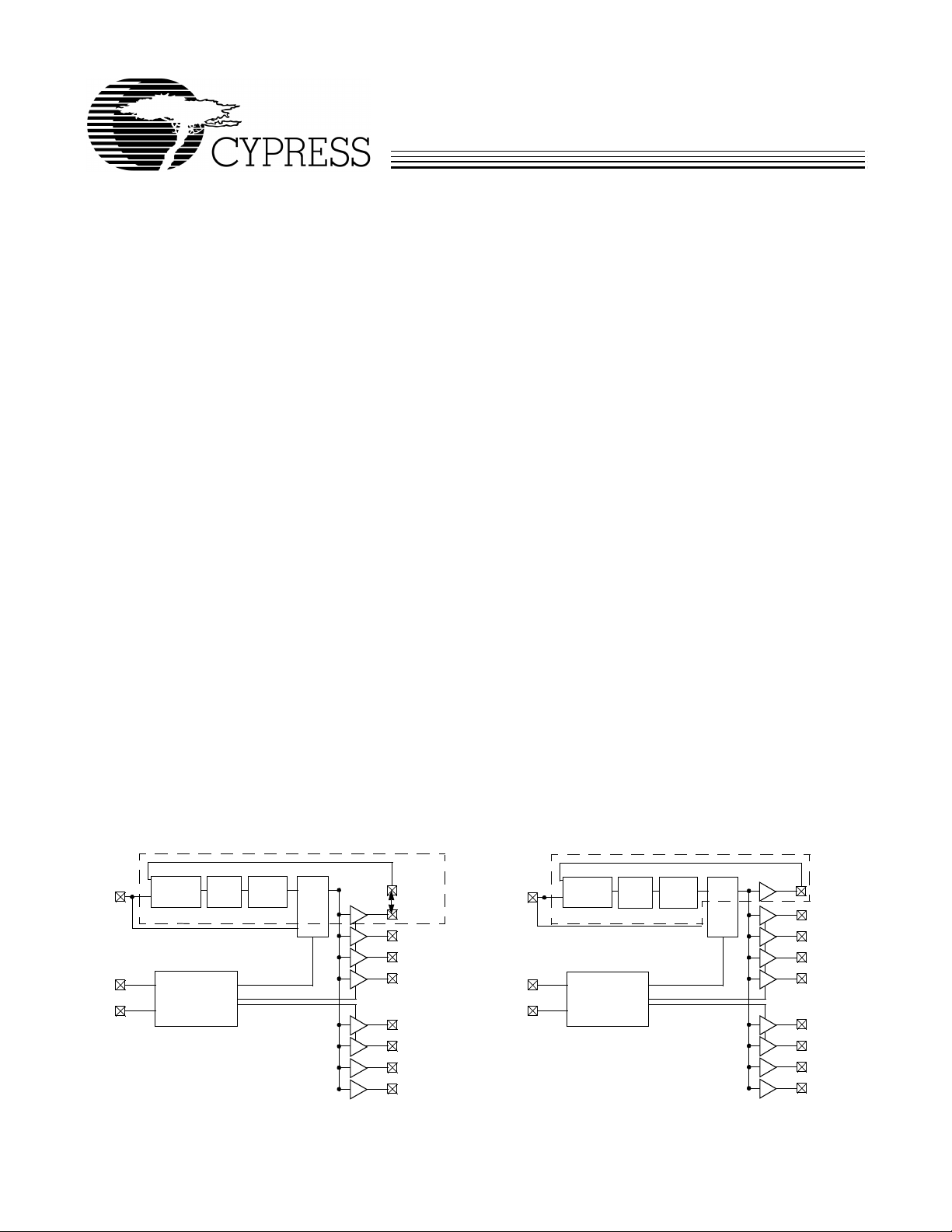
Figure 2. Simplified Block Diagram of CY2309
VCO
REF
CLKA1
CLKA2
CLKA3
CLKA4
CLKOUT
Loop
Filter
Phase
Detector
PLL
MUX
Select Input
Decoding
S2
S1
CLKB1
CLKB2
CLKB3
CLKB4
CY2305 and CY2309 as PCI and SDRAM Buffers
Introduction to Cypress Zero Delay Buffers
What is a Zero Delay Buffer?
A zero delay buffer is a device that can fan out 1 clock signal
into multiple clock signals with zero delay and very low skew
between the outputs. This de vice is well suited as a buffer for
PCI or SDRAM due to its zero input to out put delay and very
low output to output skew.
A simplified diag ram of the CY2308 zero dela y buff er is shown
in Figure 1. The CY2308 is built using a PLL that uses a ref-
erence input and a feedback input. The feedback loop is
closed by driving the feedback input (FBK) from one of the
outputs. The phase detector in the PLL adjusts the output
frequency of the VCO so that the two inputs have no phase
difference. Since an output is one of the inputs to the PLL,
zero phase difference is maintained from REF to the output
driving FBK. Now if all outputs are uniformly loaded, zero
phase difference will be maintained from REF to all outputs.
This is a simple zero delay buffer. Introducing additional devices (e.g., dividers) between the output and FBK can give
rise to some innovative applications for the PLL, and for further information on these refer to the Cypress Application
Note “CY2308 Zero Delay Buffer”. Since many buffering ap-
plications require only a simple closure of the feedback loop,
Cypress has designed zero delay buffers with Internal Feedback Loops: the CY2305 and CY2309.
What are the CY2305 and CY2309?
Cypress ha s desi gned zer o de la y b u ff ers espec iall y sui ted f or
use with PCI or SDRAM buffering. The CY2305 an d CY2309
have been designed with the feedback path integrated for
simpler system design. A simplified block diagram of the
CY2309 zero delay buffer is shown Figure 2. This zero delay
buffer uses a input/output pad on CLKOUT so that the feedback signal can be sensed directly from the out put itself .
Drive Capability
The CY2305 and CY2309 have high drive outputs designed
to meet the JEDEC SDRAM specifications of 30 pF capacitance on each DIMM clock input.
Since the typical CMOS input is 7 pF and the CY2305/09 are
designed to dri ve up to 30 pF; this means that up to 4 CMOS
inputs can be driven from a single output of a CY2305/09.
Howev er t he ou tput loadi ng o n the CY2305/ 09 mu st be equal
on all outputs to maintain zero dela y from the input.
Power Down
The CY2305 and CY2309 ha ve a unique po wer-down mode:
if the input r ef ere nce is stoppe d, the part au tomati call y en ters
a shutdown state , shutting down t he PLL and three-st ating the
outputs. When the part is in shut down mode it dr aws less t han
50 µA, and can come out of shutdown mode with the PLL
locked in less than 1 m s. This power down mode c an also be
entered by three-stating the input reference driver and al lowing the internal pull-down to pull the input LOW (the input
does not have to go LOW, it only has to stop).
5 Volt to 3.3 Volt Level Shifting
The CY2305 and CY2309 can ac t as a 5-volt to 3.3-volt level
shifter. The reference input pad is 5-volt signal-compatible.
Since many system components still operate at 5 volts, this
feature provides the capability to generate multiple 3.3-volt
clocks from a single 5-volt reference clock. This 5-volt signal-compatibility is only available on the reference pad; the
other input pads on the CY2309 are not 5-volt compati ble.
REF
Phase
Detector
Loop
Filter
VCO
PLL
Select Input
Decoding
S2
S1
Figure 1. Simplified Block Diagram of CY2308
Cypress Semiconductor Corporation • 3901 North First Street • San Jose • CA 95134 • 408-943-2600
MUX
FBK
CLKA1
CLKA2
CLKA3
CLKA4
CLKB1
CLKB2
CLKB3
CLKB4
March 25, 1997 – Revised July 29, 1997
CY2305 and CY2309 as PCI and SDRAM Buffers
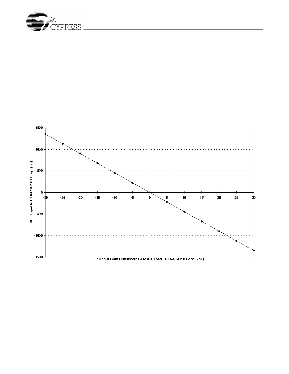
Lead or Lag Adjustments
To adjust the lead or lag of the outputs on the CY2305 or
CY2309, one must understand the relationships between
REF and CLKOUT, and the relationship between CLKOUT
and the other output s . To understa nd the r elat ionshi p , f irst w e
need to understand a few properties of the CY2305 and
CY2309 Phase Loc ked Loops. The PLL senses the pha se of
the CLKOUT pin at a threshold of V
the REF pin at the same V
/2 threshol d. All the ou tputs s tart
dd
/2 and compares it to
dd
their trans iti on at the same t ime (incl uding CLKOUT). Changing the load on an output changes its rise time and theref ore
how long it takes the output to get to the V
/2 threshold.
dd
Using these properties to our advantage, we can then adjust
the time when the outputs reach the V
to when the REF in put reaches the V
/2 threshold relative
dd
/2 threshold. T he CLK-
dd
OUT output however cannot be adjusted: it will always have
zero delay from the REF input at V
/2. The outputs can be
dd
advanced by loading the CLKOUT out put more heavily than
the other out puts or can be dela yed b y loadi ng CLKO UT more
lightly than the other outputs. Figure 3 shows how many ps
the outputs are moved vs. the difference in the loading between CLKOUT and the other outputs. As a rough guideline,
the adjustment is 50 ps/pF of loading difference. Note: the
zero delay buffer will always adjust itself to keep the V
point of the output at zero delay from the V
reference. If the application requires the outputs of the zero
/2 point of the
dd
dd
delay buffer to have zero delay from another output of the
referenc e clock chip , the output of the cloc k chip t hat is drivi ng
the zero delay buffer must be loaded the same as the other
outputs of t he cloc k chip or the output s of the zero delay buf fer
will be advanced/delayed with reference to those other outputs.
/2
Figure 3. Lead Lag Adjus tments
2
CY2305 and CY2309 as PCI and SDRAM Buffers
Output To Output Skew
The skew between CLKOUT and the other outputs is not dynamically adjusted by the loop. All MUST have the same load
on them to achieve zero output to output skew. If the other
outputs are less loaded than CLKOUT, they will lead i t; and if
the other outputs are mor e loaded, they will lag the CLKOUT.
The relationshi p that exi sts between the CLK OUT and the rest
Zero Delay Buffer Timing diagrams with different loading configurations.
REF input and all
outputs loaded equally
REF
CLKOUT
of the outputs is tha t the y all s tart the rising edge at the same
time, but different loads will cause them to have different rise
times and different times crossing the measurement thresholds. Since CLK OUT i s the only output th at is monitor ed, it will
be the output that has the zero dela y fr om the reference and
the other clocks will be relative to CLKOUT and their loading
differences.
CLKA1
CLKA4
CLKB1
CLKB4
REF input and CLKA1-CLKB4 loaded
equally, with CLKOUT loaded more
REF
CLKOUT
CLKA1
CLKA4
CLKB1
CLKB4
Zero Delay
REF input and CLKA1-CLKB4 loaded
equally, with CLKOUT loaded less
REF
CLKOUT
CLKA1
CLKA4
CLKB1
CLKB4
Advanced
Delayed
3
 Loading...