

Cypress Semiconductor CY22392ZI-xxx, CY22392ZC-xxx, CY22392FI, CY22392FC Datasheet
5
CY22392
Three-PLL General Purpose
FLASH Programmable Clock Generator
Features Benefits
Three integrated phase-locked loops Generates up to 3 unique frequencies on 6 outputs up to
200 MHz from an external source. Functional upgrade for current CY2292 family.
Ultra Wide Divide Counters (8-bit Q, 11-bit P, and 7-bit
Post Divide)
Improved Linear Crystal Load Capacitors Improves frequency accuracy over temperature, age, process,
Flash programmability Non-Volatile programming enables easy customization,
Field programmable In-house programming of samples and prototype quantities is
Low-jitter, high-accuracy outputs Performance suit able for high -end multimed ia, communicat ions,
Power-management options (Shutdown, OE, Suspend) Supports nume rous l ow- po wer a ppl ic ati on schemes and redu c-
Configurable Crystal Drive Strength Adjust Crystal Drive Strength for compatibility with virtually all
Frequency Select via 3 External LVTTL Inputs 3-Bit External Frequency Select Options for PLL1, CLKA, and
3.3V operation Industry-standard supply voltage.
16-pin TSSOP Packages Industry-standard packaging saves on board space.
CyClocksRT™ Support Easy to use software support for design entry.
Allows for 0 ppm Frequency Generati on and Frequ ency Conversion under the most demanding applications.
and initial offset.
ultra-fast turnaround, performance tweaking, design timing margin testing, inventory control, lower part count, and more secure
product supply. In addition, any part in the family can also be
programmed multiple times which reduces programming errors
and provides an easy upgrade path for existing designs.
available using the CY3672 FTG Development Kit. Production
quantities are avail able through Cypress Semic onductor’s value
added Distributio n p artners or by usi ng thi rd p ar ty prog ramme rs
from BP Microsystems, HiLo Systems, and others.
industrial, A/D Converters, and consumer applications.
es EMI by allowing unused outputs to be turned off.
crystals.
CLKB.
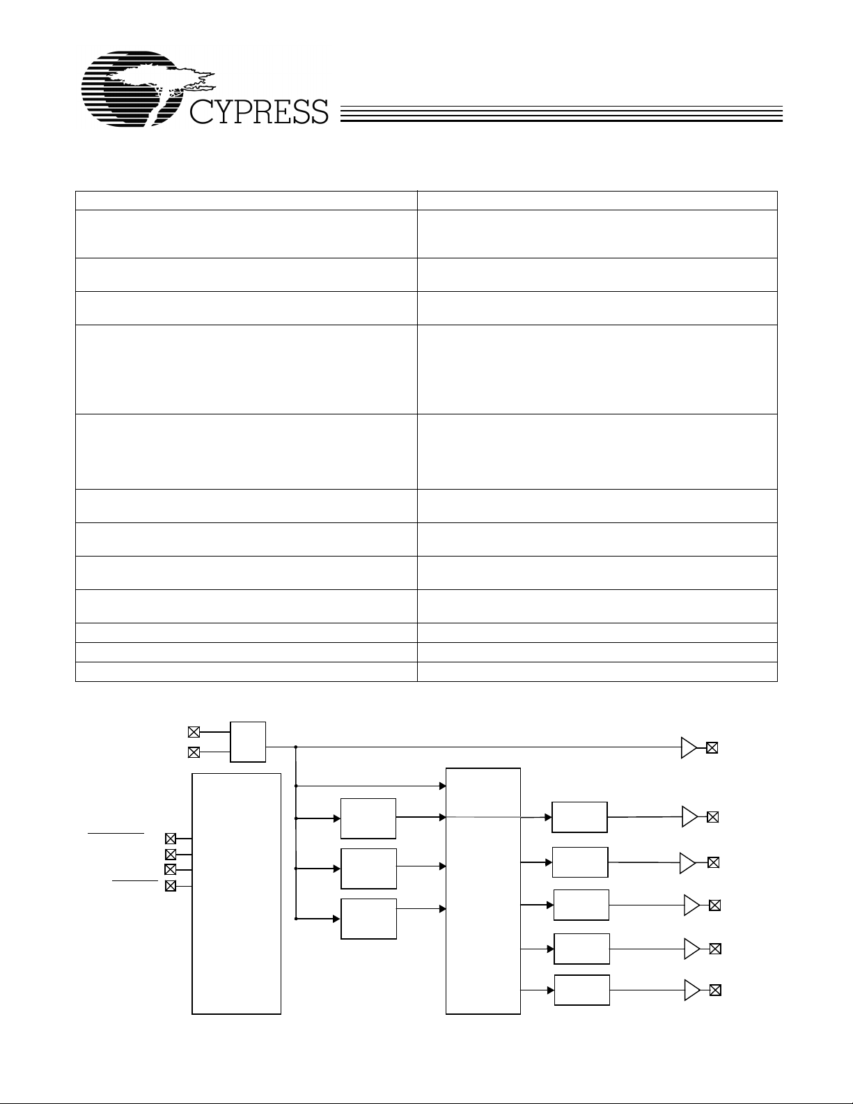
Logic Block Diagram
XTALIN
XTALOUT
CONFIGURATION
SHUTDOWN
S2/SUSPEND
CYClocks RT is a trademark of Cypress Semiconductor Corporation
/OE
S0
S1
OSC.
FLASH
PLL1
11 BIT P
8 BIT Q
PLL2
11 BIT P
8 BIT Q
PLL3
11 BIT P
8 BIT Q
4x4
Crosspoint
Switch
Divider
/2,3, or 4
Divider
7 BIT
Divider
7 BIT
Divider
7 BIT
Divider
7 BIT
Cypress Semiconductor Corporation • 3901 North First Street • San Jose • CA 95134 • 408-943-2600
Document #: 38-07013 Rev. *C Revised December 14, 2002
XBUF
CLKE
CLKD
CLKC
CLKB
CLKA
CY22392
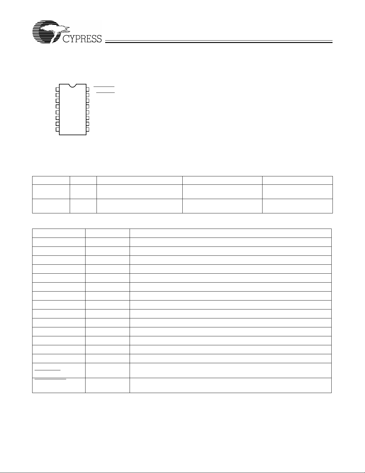
Pin Configuration
CY22392
16-pin TSSOP
CLKC
V
DD
AGND
XTALIN
XTALOUT
XBUF
CLKD
CLKE
1
2
3
4
5
6
7
8
16
15
14
13
12
11
10
9
SHUTDOWN
S2/SUSPEND
AV
DD
S1
S0
GND
CLKA
CLKB
/OE
Selector Guide
Part Number Outputs Input Frequency Range Output Frequency Range Specifics
CY22392FC 6 8 MHz–30 MHz (external crystal)
1 MHz–166 MHz (reference clock)
CY22392FI 6 8 MHz–30 MHz (external crystal)
1 MHz–150 MHz (reference clock)
Up to 200 MHz Commercial Temperature
Up to 166 MHz Industrial Temperature
Pin Summary
Name Pin Number Description
CLKC 1 Configurable clock output C
V
DD
AGND 3 Analog Ground
XTALIN 4 Reference crystal input or external reference clock input
XTALOUT 5 Reference crystal feedback
XBUF 6 Buffered reference clock output
CLKD 7 Configurable clock output D
CLKE 8 Configurable clock output E
CLKB 9 Configurable clock output B
CLKA 10 Configurable clock output A
GND 11 Ground
S0 12 General Purpose Input for Frequency Control; bit 0
S1 13 General Purpose Input for Frequency Control; bit 1
AV
DD
S2/
SUSPEND
SHUTDOWN/OE 16 Places outputs in thr ee-s tat e condit ion and sh ut s down ch ip whe n LOW. Optionally ,
2 Power supply
14 Analog Power Supply
15 General Purpose Input for Fre quency Control; bit 2. Optionally Suspe nd mode control
input.
only places outputs in tristate condition and does not shut down chip when LOW
Document #: 38-07013 Rev. *C Page 2 of 9

CY22392
Operation
The CY22392 is an upgrade to the exis ting CY 2292. The new
device has a wider frequency range, greater flexibility, improved performance, and incorporates many features that reduce PLL sensitivity to external system issues.
The device has three PLLs which, when combined with the
reference, allow up to fou r inde penden t frequ encies t o b e output on up to six pi ns. These th ree PLLs are c ompletely pr ogrammable.
Configurable PLLs
PLL1 generates a frequency that is equal to the reference divided by an 8-bi t div ider (Q) and m ultipl ied b y an 11-bit divider
in the PLL feedback loop (P). The outp ut of PLL1 is sent to the
crosspoint switch. The output of PLL1 is also sent to a /2, /3,
or /4 synchronous post-divider that is output through CLKE.
The frequency of PLL1 can be changed by external CMOS
inputs, S0, S1, S2. See the following section on General-Purpose Inputs for more details.
PLL2 generates a frequency that is equal to the reference divided by an 8-bi t div ider (Q) and m ultipl ied b y an 11-bit divider
in the PLL feedback loop (P). The outp ut of PLL2 is sent to the
crosspoint switch.
PLL3 generates a frequency that is equal to the reference divided by an 8-bi t div ider (Q) and m ultipl ied b y an 11-bit divider
in the PLL feedback loop (P). The outp ut of PLL3 is sent to the
cross-point switch.
General-Purpose Inputs
S0, S1, and S2 are general-purpose inputs that can be programmed to allow for eight different frequency settings. Options that may be switched with these general purpose inputs
are as follows; the frequency of PLL1, the output divider of
CLKB, and the output divider of CLKA.
CLKA and CLKB both have 7-bit dividers that point to one of
two programmable settings (register 0 and register 1). Both
clocks share a single register control, so both must be set to
register 0, or both must be set to register 1.
For example: the p art may be programm ed to use S0 , S1, and
S2 (0,0,0 to 1,1,1) to control eight different values of P and Q
on PLL1. For each PLL1 P and Q setting , one of the two CLKA
and CLKB divider regis ters can be chosen. A ny divider change
as a result of switching S0, S1, or S2 is guara nteed to be glitch
free.
Crystal Input
The input crystal osci llator is an important feature of thi s device
because of its flexibility and performance features.
The oscillator inverter has programmable drive strength. This
allows for maximum compatibility with crystals from various
manufacturers, processes, performances, and qualities.
The input load capacitors are placed on-die to reduce external
component cost. These capacitors are true parallel-plate capacitors for ultra-linear performance. These were chosen to
reduce the frequency shift that oc curs when non-linear load
capacitan ce in teract s wit h load , bias , supp ly, and temperature
changes. Non-linea r (FET gate) cryst al load cap acitors should
not be used f or MPEG, POTS dial tone, Comm unicati ons, or
other applications that are sensitive to absolute frequency requirements.
The value of the load capacitors is determined by six bits in a
programmable register. The load capacitance can be set with
a resolution of 0.375 pF for a total crystal load range of 6 pF
to 30 pF.
For driven clock inpu ts the input load capacitors may be com pletely bypassed . This enabl es the clock chip to acce pt driven
frequency inputs up to 166 MHz. If the application requires a
driven input, then XTALOUT must be left floating.
Output Configuration
Under normal operation there are four internal frequency
sources that may be routed via a programmable crosspoint
switch to any of the four programmable 7-bit output dividers.
The four sources are: reference, PLL1, PLL2, and PLL3. In
addition, many outputs have a unique capability for even
greater flexibilit y . The foll owing is a desc ription of each output.
CLKA’s output originates from the crossp oin t s witc h a nd g oes
through a programmable 7-bit post divider. The 7-bit post divider derives its value from one of two programmable registers. Each of the eight possible combinations of S0, S1, S2
controls which of the two programmable registers is loaded
into CLKA’s 7-bit post divider. See the section “General-Pur-
pose Inputs” for more information.
CLKB’s output origi nates from the c rossp oin t swit ch and goes
through a programmable 7-bit post divider. The 7-bit post divider derives its value from one of two programmable registers. Each of the eight possible combinations of S0, S1, and
S2 controls whic h of the two programmab le registers i s loaded
into CLKA’s 7-bit post divider. See the section “General-Pur-
pose” Inputs for more information.
CLKC’s output or iginat es from the cross point swit ch an d goe s
through a programmable 7-bit post divider. The 7-bit post divider derives its value from one programmable register.
CLKD’s output or iginat es from the cross point swit ch an d goe s
through a programmable 7-bit post divider. The 7-bit post divider derives its value from one programmable register.
CLKE’s output originates from PLL1 and goes through a post
divider that may be programmed to /2, /3, or /4.
XBUF is simply the buffered r efere nc e.
The Clock outputs have been designed to drive a single point
load with a total lumpe d load cap acita nce of 15pF. While driving multiple loads is possible with the proper termination it is
generally not recommended.
Power Saving Features
The SHUTDOWN
pulled LOW . If sy stem shut down is enabl ed, a LOW on t his pin
also shuts of f the PLLs, count ers, the referenc e oscilla tor , an d
all other active components. The resulting current on the V
pins will be less than 5 µA (typical). After leaving shutdown
mode, the PLLs will have to relock.
The S2/SUSPEND
customizable se t of outp uts a nd/or PLLs , when L OW . Al l PLLs
and any of the outputs can be shut off in nearly any combination. The only limitation is that if a PLL is shut off, all outputs
derived from it mus t a ls o b e s hut off. Suspending a PLL shuts
off all associated logic, while suspending an output simply
forces a three-state condition.
/OE input three-states the outputs when
DD
input can be configured to shut down a
Document #: 38-07013 Rev. *C Page 3 of 9
 Loading...