

Page 1
Z9973
3.3V , 125-MHz, Multi-Output Zero Delay Buffer
Features
• Output frequency up to 125 MHz
• 12 clock outputs: frequency configurable
• 350 ps max output-to-output skew
• Configurable output disable
• Two reference clock inputs for dynamic toggling
• Oscillator or PECL reference input
• Spread spectrum-compatible
• Glitch-free output clocks transitioning
• 3.3V power supply
• Pin-compatible with MPC973
• Industrial temperature range: –40°C to +85°C
• 52-pin TQFP package
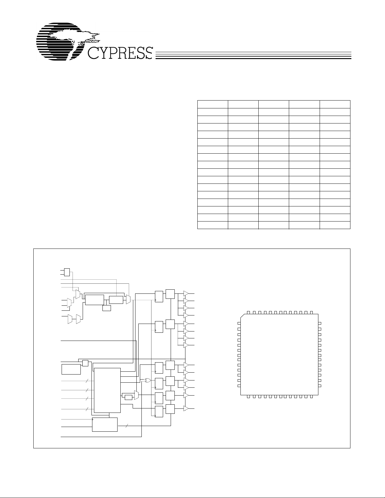
Block Diagram
PECL_CLK
PECL_CLK#
VCO_SEL
PLL_EN
REF_SEL
D
D
D
D
D
D
TCLK0
TCLK1
TCLK_SEL
FB_IN
FB_SEL2
MR#/OE
SELA(0,1)
SELB(0,1)
SELC(0,1)
FB_SEL(0,1)
SCLK
SDATA
INV_CLK
0
1
Power-On
Reset
2
2
2
2
Phase
Detector
LPF
/4, /6, /8, /12
/4, /6, /8, /10
/2, /4, /6, /8
/4, /6, /8, /10
Sync Pulse
Data Generator
Output Disable
Circuitry
VCO
0
1
0
1
/2
12
T a ble 1. Frequency Table
VC0_SEL FB_SEL2 FB_SEL1 FB_SEL0 F
[1]
VC0
00008x
000112x
001016x
001120x
010016x
010124x
011032x
011140x
10004x
10016x
10108x
101110x
11008x
110112x
111016x
111120x
Note:
1. x = the reference input frequency, 200 MHz < F
.
< 480 MHz.
VCO
Pin Configuration
Sync
Q
Frz
Sync
Q
Frz
Sync
Q
Frz
Sync
Q
Frz
Sync
Q
Frz
Sync
Q
Frz
QA0
QA1
QA2
QA3
QB0
QB1
QB2
QB3
QC0
QC1
QC2
QC3
FB_OUT
SYNC
MR#/OE
SCLK
SDATA
FB_SEL2
PLL_EN
REF_SEL
TCLK_SEL
TCLK0
TCLK1
PECL_CLK
PECL_CLK#
VCO_SEL
VDDC
QA1
QA0
VSS
52 51 50 49 48 47 46 45 44 43 42 41 40
VSS
1
2
3
4
5
6
7
8
9
10
11
12
13
VDD
14 15 16 17 18 19 20 21 22 23 24 25 26
INV_CLK
QC3
VSS
Z9973
QC2
VDDC
SELB1
SELB0
SELA1
SELA0
VDDC
QA3
QA2
VSS
VSS
39
QB0
38
VDDC
37
QB1
36
VSS
35
QB2
34
VDDC
33
QB3
32
FB_IN
31
VSS
30
FB_OUT
29
VDDC
28
27
FB_SEL0
FB_SEL1
SYNC
VSS
QC0
VDDC
QC1
SELC0
SELC1
Cypress Semiconductor Corporation • 3901 North First Street • San Jose • CA 95134 • 408-943-2600
Document #: 38-07089 Rev. *D Revised December 21, 2002
[+] Feedback
Page 2
Z9973
Pin Description
Pin Number Pin Name PWR I/O Type Pin Description
11 PECL_CLK I PU PECL Clock Input.
12 PECL_CLK# I PD PECL Clock Input.
9TCLK0 IPUExternal Reference/Test Clock Input.
10 TCLK1 I PU External Reference/Test Clock Input.
44, 46, 48, 50 QA(3:0) VDDC O Clock Outputs. See Table 2 for frequency selections.
32, 34, 36, 38 QB(3:0) VDDC O Clock Outputs. See Table 2 for frequency selections.
16, 18, 21, 23 QC(3:0) VDDC O Clock Outputs. See Table 2 for frequency selections.
29 FB_OUT VDDC O Feedback Clock Output. Connect to FB_IN for normal operation. The
25 SYNC VDDC O Synchronous Pulse Output. This output is used for system synchroni-
42, 43 SELA(1,0 ) I PU Frequency Se lect In put s. Th ese i nput s sele ct th e div ider ra tio at QA(0:3 )
40, 41 SELB(1,0 ) I PU Frequency Se lect In put s. Th ese i nput s sele ct th e div ider ra tio at QB(0:3 )
19, 20 SELC(1,0) I PU Frequency Select Input s . These in puts s elect the divi der ratio at Q C(0:3)
5, 26, 27 FB_SEL(2:0) I PU Feedback Select Inputs. These inputs select the divide ratio at FB_OUT
52 VCO_SEL I PU VCO Divider Select Input. When set LOW, the VCO output is divided by
31 FB_IN I PU Feedback Clock Input. Connect to FB_OUT for accessing the
6 PLL_EN I PU PLL Enable Input. When asserted HIGH, PLL is enabled. And when LOW,
7 REF_SEL I PU Reference Select Input. When HIG H, the crystal osc illator is selected. An d
8 TCLK_SEL I PU TCLK Select Input. When LOW , TCLK0 is selected and when HIGH TCLK1
2MR#/OE IPUMaster Reset/Output Enable Input. When ass erted LOW, res ets all of the
14 INV_CLK I PU Inverted Clock Input. When set HIGH, QC(2,3) out puts are inverted. Whe n
3SCLK IPUSerial Clock Input. Clocks data at SDATA into the internal register.
4SDATA IPUSerial Data Input. Input data is clocked to the internal register to
17, 22, 28,
33,37, 45, 49
13 VDD 3.3V Supply for PLL.
1, 15, 24, 30,
35, 39, 47, 51
Note:
2. A bypass capacitor (0.1 µF) should be placed as close as possible to each positive power (< 0.2”). If these bypass capacitors are not close to the pins, their
high-frequency filtering characteristics will be cancelled by the lead inductance of the traces.
[2]
divider ratio for this output is set by FB_SEL(0:2). See Table 1. A bypass
delay capacitor at this output will control Input Reference/ Output Banks
phase relationships.
zation. The rising edge of the output pulse is in sync with both the rising
edges of QA (0:3) and QC(0:3) output clocks regardless of the divi der ratios
selected.
outputs. See Table 2.
outputs. See Table 2.
outputs. See Table 2.
output. See Table 1.
2. When set HIGH, the divider is bypassed. See Table 1.
phase-locked loop (PLL).
PLL is bypassed.
when LOW, TCLK (0,1) is the referenc e clo ck .
is selected.
internal flip-flops and also disables all of the outputs. When pulled HIGH,
releases the internal flip-flops from reset and enables all of the outputs.
set LOW, the inverter is bypassed.
enable/disable individual outputs. This provides flexibility in power
management.
VDDC 3.3V Power Supply for Output Clock Buffers.
VSS Common Ground.
Document #: 38-07089 Rev. *D Page 2 of 9
[+] Feedback
Page 3
Z9973
Functional Description
The Z9973 has an integrat ed PL L that prov ides low -ske w and
low-jitter clock output s for high-performa nce microproc essors.
Three independent banks of four outputs as well as an
independent PLL feedback output, FB_OUT, provide exceptional flexibility for possible output configurations. The PLL is
ensured stable operation given that the VCO is configured to
run between 200 MHz to 480 MHz. This allows a wide range
of output frequencies up to125 MHz.
The phase detector co mp ares the inp ut referen ce cloc k to the
external feedback input. For normal operation, the external
feedback input, FB_IN, is connected to the feedback output,
FB_OUT. The internal VCO is runnin g at mu ltiple s of the input
reference clock set by FB_SEL(0:2) and VCO_SEL select
Table 2. Frequency Select Inputs
VCO_SEL SELA1 SELA0 QA SELB1 SELB0 QB SELC1 SELC0 QC
0 0 0VCO/80 0VCO/80 0VCO/4
0 0 1VCO/120 1VCO/120 1 VCO/8
0 1 0VCO/161 0VCO/161 0VCO/12
0 1 1VCO/241 1VCO/201 1VCO/16
1 0 0VCO/40 0VCO/40 0VCO/2
1 0 1VCO/60 1VCO/60 1VCO/4
1 1 0VCO/81 0VCO/81 0VCO/6
1 1 1VCO/121 1VCO/101 1 VCO/8
inputs (see Table 1). The VCO frequency is then divided to
provide the required output frequencies. These dividers are
set by SELA(0,1), SELB(0,1), SELC(0,1) select inputs (see
Table 2). For situations in which the VCO needs to run at
relatively low frequencies and hence might not be stable,
assert VCO_SEL LOW to d ivide the VCO frequency by 2. This
will maintain the desired output relationships, but will provide
an enhanced PLL lock range.
The Z9973 is also capable of providing inverted output clocks.
When INV_CLK is asserted HIGH, QC2 and QC3 output
clocks are inverted. These clocks could be used as feedback
outputs to the Z9973 or a secon d PLL device to generate earl y
or late clocks for a specific design. This inversion does not
affect the output to output skew.
Zero Delay Buffer
When used as a ze ro de lay bu ff er, the Z9973 will likely be i n a
nested clock tree application. For these applications the
Z9973 offers a low-voltage PECL clock input as a PLL
reference. This allows the user to us e LVPECL as the primary
clock distribution device to take advantage of its far superior
skew performance. The Z9973 can then lock onto the LVPECL
reference and translate with near-zero delay to low-skew
outputs.
By using one of the outputs as a feedback to the PLL, the
propagation delay through the device is eliminated. The PLL
works to align the output edge with the input reference edge
thus producing near-zero delay. The reference frequency
affects the static phase offset of the PLL and thus the relative
delay between inputs and outputs. Because the static phase
offset is a function o f the referenc e clock, the Tpd of t he Z9973
is a function of the configuration used.
Glitch-Free Output Frequency Transitions
Customarily, when output buffers have their internal counters
changed “on the fly,” their output clock periods will:
1. contain short or “runt” clock perio ds. These are clock cy cles
in which the cycle(s) are shorter in period than either the
old or new frequency to which it is being transitioned.
2. contain stretched clock periods. These are clock cycles in
which the cycle(s) are longer in period than either the old
or new frequency to which it is being transitioned.
This device specifically includes logic to guarantee that runt
and stretched clock pulses do not occur if the device logic
levels of any or all of the following pins changed “on the fly”
while it is operating: SELA, SELB, SELC, and VCO_SEL.
SYNC Output
In situations where output frequency relationships are not
integer multiples of each other, the SYNC output provides a
signal for system synchronization. The Z9973 monitors the
relationship between the QA and the QC output clocks. It
provides a low-going pulse, one p eriod in durat ion, one peri od
prior to the coincident ri sin g edges of th e QA and Q C out put s.
The duration and the placement of the pulse depend on the
higher of the QA and QC output frequencies. The following
timing diagram illustrates various waveforms for the SYNC
output (see Figure 1). Note. The SYNC output is defined for
all possible combinations of the QA and QC outputs even
though under some relationships the lower frequency clock
could be used as a synchronizing signal.
Document #: 38-07089 Rev. *D Page 3 of 9
[+] Feedback
Page 4

VCO
QA
QC
SYNC
QA
QC
SYNC
QC
QA
SYNC
Z9973
1:1 Mode
2:1 Mode
3:1 Mode
3:2 Mode
QA
QC
SYNC
QC
QA
SYNC
QA
QC
SYNC
QA
QC
SYNC
4:1 Mode
4:3 Mode
6:1 Mode
Figure 1. Sync Output Waveforms
Document #: 38-07089 Rev. *D Page 4 of 9
[+] Feedback
Page 5

Z9973
Power Management
The individual output enable/freeze control of the Z9973
allows the user to implement unique power management
schemes into the desig n. The outp uts are stoppe d in the logi c
“0” state when the freeze con trol bit s are ac tiv ate d. The seri al
input register cont ains one program mable freeze enabl e bit for
12 of the 14 output clocks. The QC0 and FB_OUT outputs
cannot be frozen with the serial port, which avoids any
potential lock-up si tuat ion sho uld an e rror occu r in load ing the
Start
D0 D1 D2 D3 D4 D5 D6 D7 D8 D9 D10 D11
Bit
D0-D3 are the control bits for QA0-QA3, respectively
D4-D7 are the control bits for QB0-QB3, respectively
D8-D10 are the control bits for QC1-QC3, respectively
D11 is the control bit for SYNC
Figure 2. SDATA Input Register
serial data. An output is frozen whe n a logic “0” is programmed
and enabled when a logic “1” is written. The enabling and
freezing of individual outputs is done in such a manner as to
eliminate the possibility of partial “runt” clocks.
The serial input register is programmed through the SDATA
input by writing a logic “0” start bit followed by 12 NRZ freeze
enable bits (see Figure 2). The period of each SDATA bit
equals the period of the free-running SCLK signal. The SDAT A
is sampled on the rising edge of SCLK.
Document #: 38-07089 Rev. *D Page 5 of 9
[+] Feedback
Page 6

Z9973
Maximum Ratings
Maximum Input Voltage Relative to VSS:............ VSS – 0.3V
Maximum Input Voltage Relative to VDD:.............VDD + 0.3V
Storage Temperature: ................................–65°C to + 150°C
Operating Temperature:................................–40°C to +85°C
Maximum ESD protection...............................................2 kV
Maximum Power Supply:................................................5.5V
Maximum Input Curr ent:..................................................±20 mA
DC Parameters (V
[3]
= 2.9V to 3.6V, V
DD
This device contains circuitry to protect the inputs against
damage due to high static voltages or electric field; however,
precautions should be taken to avoid application of any
voltage higher tha n the maximum rate d voltages to thi s circuit.
For proper operation, V
the range:
< (VIN or V
V
SS
Unused inputs must always be tied to an appropriate logic
voltage level (either V
= 3.3V ±10%, TA = –40°C to +85°C)
DDC
OUT
and V
IN
) < VDD .
or VDD).
SS
should be constrained to
OUT
Parameter Description Conditions Min. Typ. Max. Unit
V
IL
V
IH
V
PP
V
CMR
I
IL
I
IH
V
OL
V
OH
I
DDQ
I
DDA
I
DD
Input LOW Voltage V
SS
Input HIGH Voltage 2.0 V
Peak-to-Peak Input Voltage
300 1000 mV
0.8 V
DD
PECL_CLK
Common Mode Range PECL_CLK
Input Low Current
Input High Current
Output Low Voltage
Output High Voltage
[10]
[10]
[11]
[11]
[9]
V
– 2.0 V
DD
– 0.6 V
DD
–120 µA
120 µA
IOL = 20 mA 0.5 V
IOH = –20 mA 2.4 V
Quiescent Supply Current 10 15 mA
PLL Supply Current VDD only 15 20 mA
Dynamic Supply Current QA and QB @ 60 MHz,
225 mA
QC @ 120 MHz, CL = 30 pF
QA and QB @ 25 MHz,
125
QC @ 50 MHz, CL = 30 pF
C
IN
Input Pin Capacitance 4 pF
V
AC Parameters (V
= 2.9V to 3.6V , V
DD
= 3.3V ±10%, TA = –40°C to +85°C)
DDC
[4]
Parameter Description Conditions Min. Typ. Max. Units
Tr / Tf TCLK Input Rise / Fall 3.0 ns
Fref Reference Input Frequency Note 5 Note 5 MHz
FrefDC Reference Input Duty Cycle 25 75 %
Fvco PLL VCO Lock Range 200 480 MHz
Tlock Maximum PLL Lock Time 10 ms
Tr / Tf Output Clocks Rise/Fall Time
Notes:
3. The voltage on any input or I/O pic cannot exceed the power pin during power-up. Power supply sequencing is NOT required.
4. Parameters are guaranteed by design and characterization. Not 100% tested in production.
5. Maximum and minimum i nput reference is limited by VC0 lock range.
6. Outputs loaded with 30 pF each.
[6]
0.8V to 2.0V 0.15 1.2 ns
Document #: 38-07089 Rev. *D Page 6 of 9
[+] Feedback
Page 7

Z9973
AC Parameters (V
= 2.9V to 3.6V , V
DD
= 3.3V ±10%, TA = –40°C to +85°C) (Continued )
DDC
[4]
Parameter Description Conditions Min. Typ. Max. Units
Fout Maximum Output Frequency Q (÷2) 125 MHz
Q (÷4) 120
Q (÷6) 80
Q (÷8) 60
FoutDC Output Duty Cycle
tpZL, tpZH Output Enable Time
tpLZ, tpHZ Output Disable Time
TCCJ Cycle to Cycle Jitter
TSKEW Any Output to Any Output Skew
Propagation Delay
[6]
[6]
(all outputs) 2 10 ns
[6]
(all outputs) 2 8 ns
(peak to peak)
[7,8]
[6]
[6,7]
TCYCLE
/2 – 750
TCYCLE
/2 + 750
± 100 ps
250 350 ps
–225 –25 175 ps
ps
Tpd QFB = (÷8) –70 130 330
–130 70 270
Ordering Information
Part Number Package Type Production Flow
IMIZ9973BA 52-pin TQFP Industrial, –40°C to +85°C
IMIZ9973BAT 52-pin TQFP–Tape and Reel Industrial, –40°C to +85°C
Notes:
7. 50Ω transmission line terminated into VDD/2.
8. Tpd is specified for a 50-MHz input reference. Tpd does not include jitter.
9. The VCMR is the difference from the most positive side of the differential input signal. Normal operation is obtained when the “High” input is within the VCMR
range and the input lies within the VPP specification.
10. Inputs have pull-up/pull-down resistors that effect input current.
11. Driving series or parallel terminated 50Ω (or 50Ω to VDD/2) transmission lines.
Document #: 38-07089 Rev. *D Page 7 of 9
[+] Feedback
Page 8

ng so indemnifies Cypress Semiconductor against all charges.
Package Drawing and Dimensions
52-lead Thin Plastic Quad Flat Pack (10 × 10 × 1.4 mm) A52
Z9973
51-85131-**
All product and company names mentioned in this document are the trademarks of their respective holders.
Document #: 38-07089 Rev. *D Page 8 of 9
© Cypress Semiconductor Corporation, 2002. The information contained herein is subject to change without notice. Cypress Semiconductor Corporation assumes no responsibility for the use
of any circuitry other than cir cuitry embodi ed in a Cypress S emiconductor product . Nor does it convey or imply any license un der patent or other righ ts. Cypre ss Semiconductor does not autho rize
its products for use as critical components in life-support systems where a malfunction or failure may reasonably be expected to result in significant injury to the user. The inclusion of Cypress
Semiconductor products in life-support systems application implies that the manufacturer assumes all risk of such use and in doi
[+] Feedback
Page 9

Document Title: Z9973 3.3V, 125 MHz Multi-Output Zero Delay Buffer
Document Number: 38-07089
Rev. ECN No. Issue Date
** 107125 06/06/01 IKA Convert from IMI to Cypress
*A 108067 07/03/01 NDP Changed Commercial to Industrial
*B 111799 02/06/02 BRK Convert from Word Doc to Adobe Framemaker Cypress Format
*C 116452 07/30/02 HWT Corrected the Ordering Information to match the DevMaster.
*D 122774 12/21/02 RBI Add power up requirements to maximum ratings information.
Orig. of
Change Description of Change
Changed the Timing Diagram and the operating voltage condition
Z9973
Document #: 38-07089 Rev. *D Page 9 of 9
[+] Feedback
 Loading...