

Spread Spectrum Frequency Timing Generator
W42C32-05
Cypress Semiconductor Corporation
• 3901 North First Street • San Jose • CA 95134 • 408-943-2600
September 28, 1999, rev. **
Features
• Maximized EMI suppression usi ng Cypress’s Spread
Spec t r u m techno logy
• Generates a spread spectrum timing signal
• Reduces measured EMI by as much as 12 dB
• Integrated loop filter components
• Requires a single lo w -cost fundament al crystal (or
other frequency reference) for proper operation
• Special spread spectrum control functions
• Low-power CMOS design
• Av ailable in 16-pin SOIC package, (300 mil)
Overview
The W42C32 modulat es the output of a single PLL in order to
‘spread’ the bandwidth of a synthesized clock and, more importantly, decrease the peak amplitudes of its fundamental
harmonics. Since peak amplitudes are reduced, the radiated
electromagnet ic e missio ns o f the W42C32- 05 ar e s ignif icant ly
lower t han the typical narrow band signal produced by oscillators and most frequency generators. Lowering a signal’s amplitude by increasing its bandwidth is a method of reducing
EMI called ‘spread spectrum frequency timing generation’.
This patented techni que not only reduces the emis sions of the
primary clock, bu t also impact s ev ery signal synchroniz ed to it.
Key Specifications
Cycle-to-Cycle Jitter ....................................................250 ps
45/55 Duty Cycle.................................... approximately 1.4V
Selectable Frequency spread
2 ns rise/fall time 0.4V to 2.0V, 3.3V supply
2 ns rise/fall time 0.8V to 2.4V, 5.0V supply
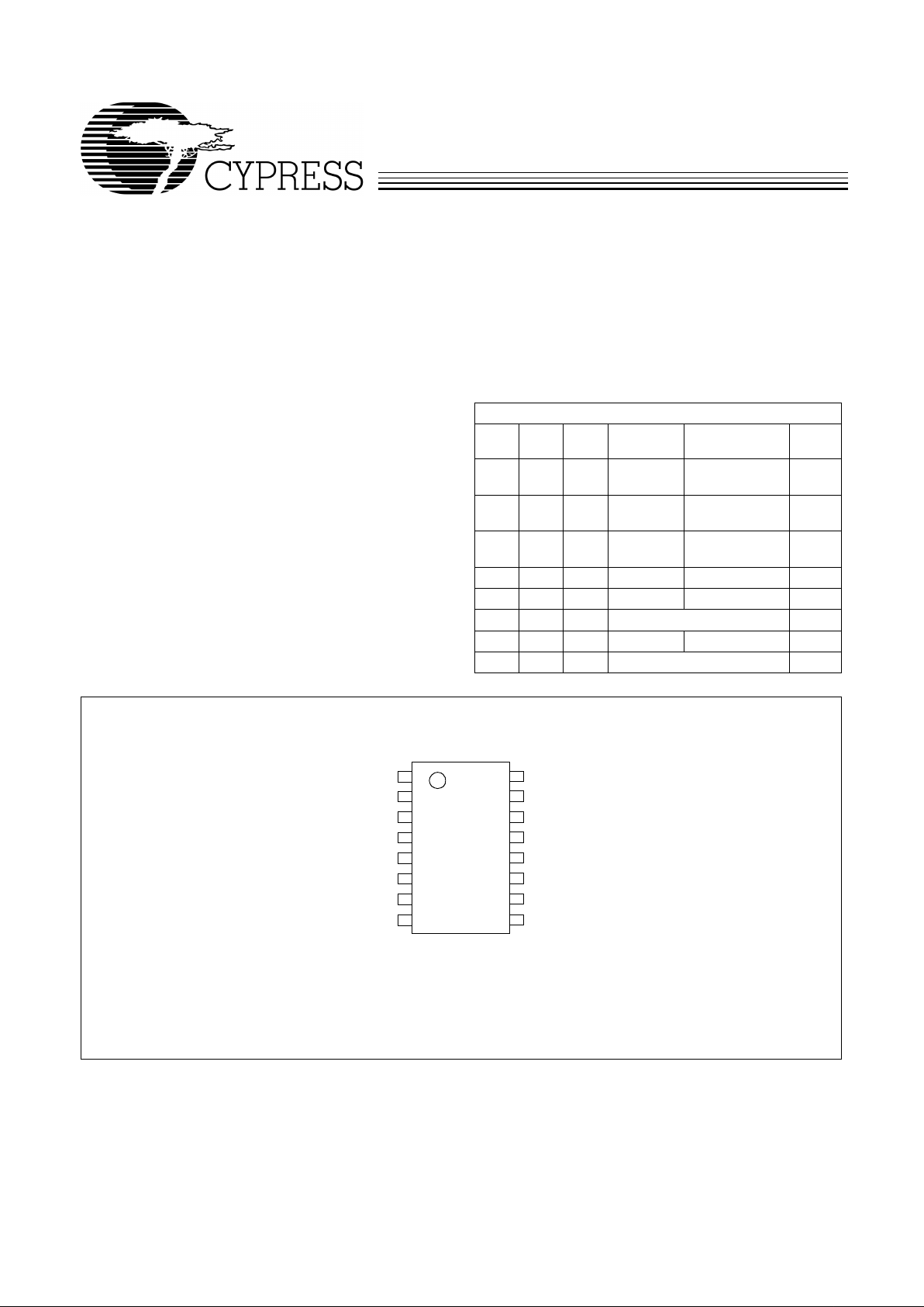
T able 1. Frequency Spread Selection
W42C32-05
FS2 FS1 FS0
REFOUT
(MHz)
CLKOUT
(MHz)
VDD
(V)
0 0 0 22.1148 44.2296 ±
2.5%
5.0
0 0 1 22.1148 44.2296
±1.5%
5.0
0 1 0 14.7456 29.4912 ±
2.5%
5.0
0 1 1 18.432 18.432 ± 2.5% 5 .0
1 0 0 14.318 66.66 – 2% 3.3
1 0 1 Reserved 3.3
1 1 0 14.318 100 – 2% 3.3
1 1 1 Reserved 3.3
Pin Configuration
W42C32-05
16
15
14
13
12
11
10
9
1
2
3
4
5
6
7
8
PD#
X1
X2
GND
AGND
FS0
TEST
CLKOUT
REFOUT
FS2
FS1
SSON#
RESET
VDD
AVDD
REFEN#
SOIC
W42C32-05
2
Pin Definitions
[1]
Pin Name Pin No.
Pin
T ype Pin Description
CLKOUT 8 O
Output Modulated Frequency
: Frequency is set using FS0:2 (refer to Table 1).
REFOUT 16 O
Reference Output:
A buffered version of the input frequency.
X1 2 I
Crystal Connection or External Reference Frequency Input :
This pin has dual functions. It c an b e used a s ei ther an e xt ernal crystal con nectio n, or as an e xt ernal ref er enc e
frequency input.
X2 3 I
Crystal Connection:
If using an external reference, this pin must be left unconnecte d.
SSON# 13 I
Spread Spe ctrum Contro l (active LO W):
Pulling this input s ignal HIGH turns the internal
modulating wa veform off. This pin has an inte rnal pull-down resistor.
FS0 6 I
Frequency Select ion Bit 0:
This pin selects t he frequency and spreadi ng characteri stics.
Refer to Tabl e 1 . This pin has an internal pull-up resistor.
FS1 14 I
Frequency Select ion Bit 1:
This pin selects t he frequency and spreadi ng characteri stics.
Refer to Tabl e 1 . This pin has an internal pull-up resistor.
FS2 15 I
Frequency Select ion Bit 2:
This pin selects t he frequency and spreadi ng characteri stics.
Refer to Tabl e 1 (note the V
DD
specific ation). This pin has an internal pull-up resistor.
PD# 1 I
Po wer-down (active LOW):
Enabling power-down reduces current consumption and
disables the clock outputs. This pin has an internal pull-up resistor.
REFEN# 9 I
Reference Cloc k Selection Input:
Pulling this signal LOW turns the REFOUT cloc k
output on. This pin has an inter nal pull-up resistor.
RESET 12 I
Reset:
A reset starts the spread spec trum modulating frequency at the beginnin g point
of the modulation pr of ile . This pin has an i nternal pull -do wn resi stor. T o reset the spread
spectrum modulating frequency, pull thi s pin from LO W to HIGH.
VDD 11 P
Po wer Connection:
Connected to either 3.3V or 5.0V po wer supply . V
DD
and A VDD must
be the same voltage le vel.
AVDD 10 P
Analog Power Connection:
Connected to ei ther 3.3V or 5.0V power supply. V
DD
and
AV
DD
must be the same voltage level.
GND 4 G
Ground Connection :
Connect to the common system ground plane.
AGND 5 G
Analog Ground Connection:
Connect to the common system ground plane.
TEST 7 I
Three-state Input:
Pulling this input pin and REFEN# pin HI GH, CLKOUT will be
three-stated. This pin has an internal pull-down resistor.
[2]
Notes:
1. Pull-up resistors not CMOS level.
2. Pulling PD# and REFEN# input pins HIGH, REFOUT will be three-stated.
W42C32-05
3
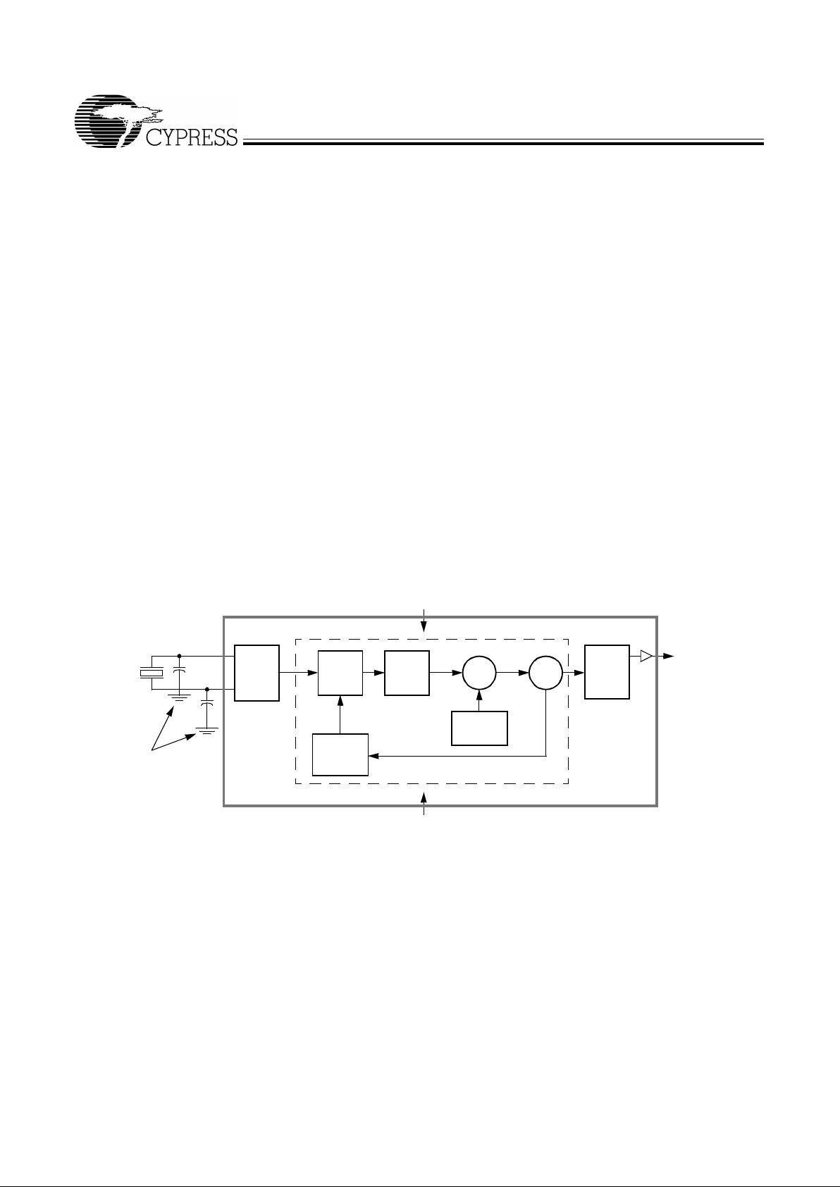
Functional Description
The W42C32-05 uses a phase-locked loop (PLL) to multiply
the frequency of a low-cost, low-frequency cr ystal up to the
desired cl ock f req uency. The basic c ircuit top olog y is s ho wn i n
Figure 1. An on- chip crystal driver causes the crystal to osci llate at its fundamental. The resulting reference signal is divided by Q and fed to the phase detector. The VCO output is
divided by P and also fed back to the phase detect or . The PLL
will force the frequency of the VCO output signal to change
until the divi ded output signal and the di vided re f erenc e signal
match at the phase detector input. The output frequency is
then equal to the ratio of P/Q times the reference frequency.
The unique feature of the Spr ead Spec trum F requ ency Timin g
Generator is that a modulating waveform is superimposed at
the input to the VCO . Thi s causes t he VCO ou tput to b e sl ow ly
swept across a predetermined frequency band.
Because the modulating frequency is typically 1000 times
slower than the fundamental clock, the spread spectrum process has little impact on system performance.
Frequency Selecti on W it h SSFTG
In Spread Spectr um frequency timing generat ion, EMI reduction depends on the shape, modulation percentage, and frequency of the modulating waveform. While the shape and frequency of the modulating waveform in the W42C32 are fixed,
the modulati on percentage may be varied.
Using frequency select bits (FS2:0 pins), various spreading
percentages for different input frequency ranges can be chosen. For example, refer to the W42C32-05 in Ta b l e 1. If the
logic level on FS2:0 = 000, then an input reference frequency
between 14 and 24 MHz will produce an output frequency at
twice the reference frequency with a spread of ±2.5%.
A larger spreading per centage improves EMI reduction. However, large spread percentages may either exceed system
maximum frequ ency ra tings or lo wer the a v erag e fr equency t o
a point where performance is affected. For these reasons,
spreading percentages between ±0.875% and ±2.5% are
most common.
Additional Features of the W42C32-05
A RESET pin is available to aid in applications which have
multiple PLL clock generators. When a reset is issued, the
modulation profile shown in Figure 3 is reset to its starting
point. This feature is necessary for applications in which two
spread spectrum systems must synchr onize with each other.
The REFOUT out pin provi des a buffered version of the input
clock frequency.
The SSON# pin disables the spread spectr um function when
set to logic HIGH. Otherwi se, an internal pull-down resistor
leaves this feature enab led.
The PD# pin reduces power consumption and disables the
clock output s when set to logic LOW. Otherwise, an internal
pull-up resistor places the W42C32-05 into normal mode .
Figure 1. System Block Diagra m (Co ncept, not actual impl eme ntat ion)
XTAL
Freq.
Phase
Modulating
VCO
Post
CLKOUT
Detector
Charge
Pump
Waveform
DividersDivider
Feedback
Divider
PLL
GND
V
DD
X1
X2
Crystal load
capacitors
as needed
Σ
Q
P

W42C32-05
4
Spread Spectrum Frequency Tim ing
Generation
The benefits of using Spread Spectrum Frequency Timing
Generation are depicted in Figure 2. An EMI emission profile
of a clock harmonic is shown.
Contrast the typical clock EMI with the Cypress spread spectrum clock. Noti ce t he spik e in th e typi cal cl oc k. Thi s spi k e can
make sys tems fail quasi-peak EMI test ing. The FCC an d other
regulatory agencies test for peak emissions. With Cypress’s
Spread Spectrum Frequency Timing Generator (SSFTG), the
peak energy i s much lower (at leas t 8 dB) becaus e the energ y
is spread out across a wider bandwidth.
Modulating Waveform
The shape of the modul ating wa vef orm is critica l to EMI reduction. The modulation scheme used to accomplish the maximum reduction in EMI is shown in Figure 3. The period of the
modulation is shown as a percentage of the period length
along the X axis. The amount that the frequency is varied is
shown along the Y axis, also shown as a percentage of the
total frequency spread.
Cypress frequency selection tables express the modulation
percentage in two wa y s. The firs t method di spla y s the spr eading frequency band as a percent of the programmed average
output frequency, symmetric about the programmed average
frequency. This method is always sho w n using the expression
f
Center ± XMOD
% in the frequency spread selection table.
The second approach is to specify the maximum operati ng
frequency and th e spreadi ng band as a percent age of this fr equency. The output signal is swept from the lower edge of the
band to the maximum frequency. The expression for this approach is f
MAX – XMOD
%. Whenever this expression is used,
Cypress has taken care to ensure that f
MAX
will never be exceeded. This is important in applications where the clock
drives componen ts with tight maxi mu m clock sp eed spec ifi cations.
SSFTG
Typical Clock
5dB/div
Amplitude (dB)
Figure 2. Typical Clo ck and SSFTG Comparison
100%
60%
20%
80%
40%
0%
–20%
–40%
–60%
–80%
–100%
10%
20%
30%
40%
50%
60%
70%
80%
90%
100%
10%
20%
30%
40%
50%
60%
70%
80%
90%
100%
Time
Frequency Shift
Figure 3. Modulation W aveform Profile

W42C32-05
5
Absolute Maximum Ratings
Stresses gre ater th an those list ed i n this tab le may cause permanent damage to the de vice. These represent a str ess ratin g
only. Operation of the device at these or any other conditions
above those specified in the operat ing sections of this specifi cation is not implied. Maximum conditions for extended periods may affect reliability.
Parameter Description Rating Unit
V
DD
, V
IN
V oltage on any pin with respect to GND –0.5 to +7 .0 V
T
STG
Storage Temperature –65 to +150 °C
T
A
Operating Temperature 0 to +70 °C
T
B
Ambient Temperature under Bias –55 to +125 °C
DC Electr i cal C h ar acteristics :
0°C < T
A
< 70°C, VDD = 5.0V±10%, 3.3V±5%
Parameter Description T est Condi tion Min T yp Max Unit
I
DD
Supply Current V
DD
= 5.0, 100 MHz 35 45 mA
t
OFF
Power Down Time 4 cycles
[3]
t
ON
Power Up Tim e F irst locked cl ock cycle after
PD# goes HIGH
5ms
t
EN
Enable/Dis able Time Time required for output t o be
enabled/disabled
4cycles
[3]
V
IL
Input Low Voltage VDD = 5.0V 0.8 V
V
DD
= 3.3V 0.15V
DD
V
V
IH
Input High Voltage VDD = 5.0V 3.0 V
V
DD
= 3.3V 0.7V
DD
V
V
OL
Output Low Voltage 0.4 V
V
OH
Output High Voltage VDD = 5.0V 2.4 V
V
DD
= 3.3V 2.4 V
I
IL
Input Low Cur rent –100
µ
A
I
IH
Input High Current 10
µ
A
I
OL
Output Low Current @ 0.4V, VDD = 3.3V 2.4 mA
I
OH
Output High Current @ 2.4V, VDD = 3.3V 2.4 mA
C
I
Input Capacitance All pins exce pt X1, X2 7 pF
C
L
XTAL Load Capacitance Pins X1, X2 16 pF
R
P
Input Pull-Up Resistor VIN = 0V 300 kΩ
Z
OUT
Clock Output Impedance Any clock output pin 33 Ω
Note:
3. Cycle refers to input clock cycles supplied by the input crystal or reference.

W42C32-05
6
AC Electrical Characteristics:
TA = 0°C to +70°C, VDD = 5V±10%. 3.3V±5%
Symbol Parame ter Test Condition Min Typ Max Unit
f
IN
Input Frequency 12 28 MHz
f
OUT
Output Frequency 18 100 MHz
t
R
Output Rise Time 15-pF load 0.4V–2.4V 1 2 ns
t
F
Output Fall Time 15-pF load 2.4V–0.8V 1 2 ns
t
OD
Output Duty Cycle 15-pF load, VDD = 5.0V 45 55 %
t
OD
Output Duty Cycle 15-pF load, VDD = 3.3V 40 60 %
t
ID
Input Duty Cycle 40 60 %
t
JCYC
Jitter, C y cle-to-Cycle 250 300 ps
Harmonic Reduction f
in
= 16 MHz, ninth harmonic meas ured,
reference board, 15-pF load
8dB

W42C32-05
7
Application Information
Recommended Circuit Configuration
For optimum performance in system applic ations t he power
supply decoupli ng scheme show n in Figure 4 should be used.
V
DD
decoupling is important to both reduce phase jitter and
EMI radiation. The 0.1-µF decoupling capacitor should be
placed as close to the V
DD
pin as possible, otherwise the in-
creased tr ace inductance will negate its decoupling capability.
The 10-µF decoupling capacitor shown should be a tantalum
type. For further EMI protection, the V
DD
connection can be
made via a ferrite bead, as shown.
The 16-pF XTAL load capacitors can be u sed to r aise t he inte -
grated 12-pF capacitors up to a total load of 20 pF on the
crystal.
Recommended Board Layout
Figure 4 shows a recommended 2-layer board layout .
Document #: 38-00808
Ordering Information
Ordering Code
Freq. Mask
Code
Package
Name
Packag e Type
W42C32 05 G 16-pin Plastic SOIC (300-mil)
Figure 4. Recommended Board Layout (2-Layer Board)
C1 =16 pF
C
2
= 16 pF
XTAL1
Typical value is 16 pF.
High frequency supply decoupling
capacitor (0.1-
µF recommended).
Common supply low frequency
decoup ling capacitor (10-
µF tantalum
recommended).
XTAL load capacitors.C1, C2 =
C3, C5, C6 =
C4 =
Match value to line impedance.
33Ω =
33
Ω
CLKOUT
33
Ω
(Modulated Output)
C4 = 10 µF
C3 = 0.1 µF
REFOUT
Ground
Ground
Fer r ite Bea d
Voltage Supply Input
(3.3V, 5.0V)
1
2
3
4
5
6
7
8
16
15
14
13
12
11
10
9
G
G
G
C5
G
C6
(Via to ground plane)

W42C32-05
© Cypress Semiconductor Corporation, 1999. The information contained herein is subject to change without notice. Cypress Semiconductor Corporation assumes no responsibility for the use
of any circuitry other than circuitry embodied in a Cypress Semiconductor product. Nor does it con vey or imply any license under patent or other rights. Cypress Semiconductor does not authorize
its products for use as critical components in life-support systems where a malfunction or failure may reasonably be expected to result in significant injury to the user. The inclusion of Cypress
Semiconductor products in life-support systems application implies that the manufacturer assumes all risk of such use and in doing so indemnifies Cypress Semiconductor against all charges.
Package Diagram
16-Pin Small Outline Integrat ed Circuit (SOIC, 300-mil)
 Loading...