W40S11-23
Clock Buffer/Driver
Features
• Thirteen skew-controlled CMOS clock outputs
(SDRAM0:12)
• Supports three SDRAM DIMMs
• Ideal for hi gh-performance system s designed around
Intel’s latest chip set
2
C serial configuration interface
•I
• Clock Skew between a ny two outputs is less than 250 ps
• 1- to 5-ns propag ation delay
• DC to 133-MHz opera tion
• Single 3.3V supply voltage
• Low power CMOS design pa ckaged i n a 28-pi n, 300-mil
SOIC (Small Outline Integrated Circuit)
Overview
The Cypress W40S11-23 is a low-voltage, thirteen-output
clock buffer. Output buffer impedance is approximately 15Ω,
which is ideal for driving SDRAM DIMMs.
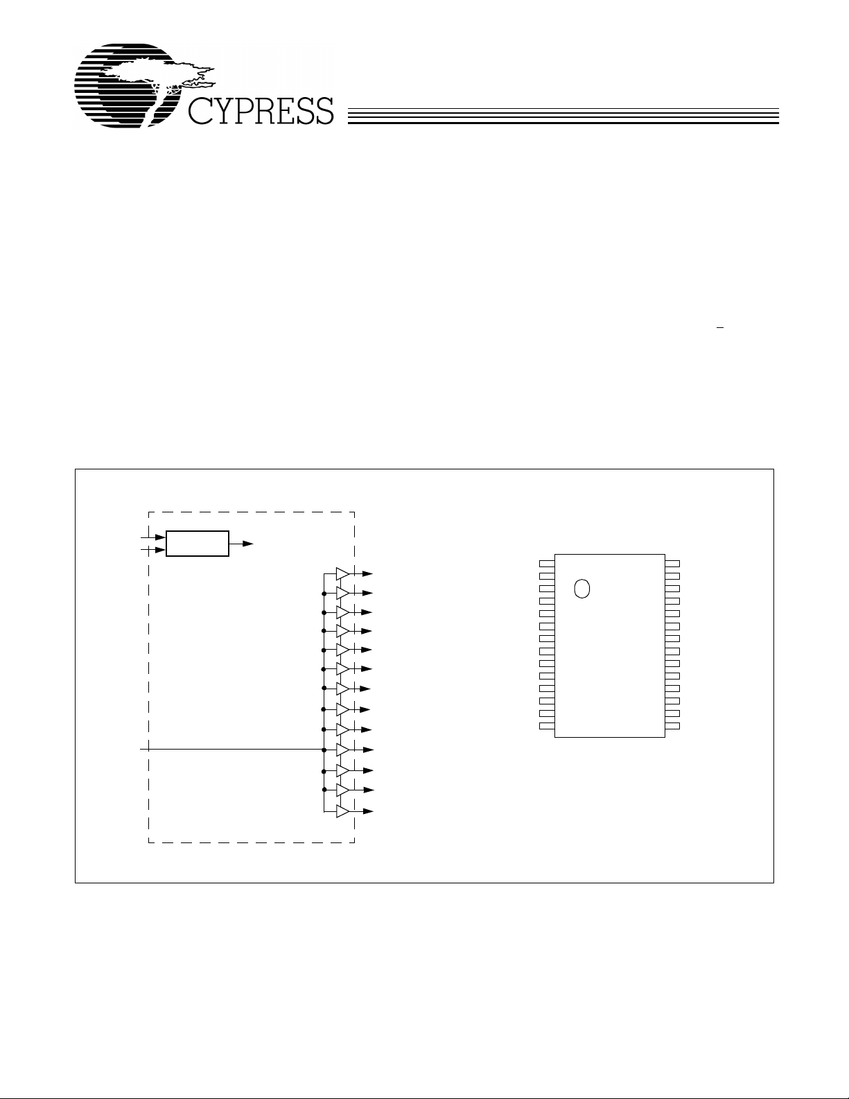
Block Diagram
SDATA
SCLOCK
BUF_IN
Serial Port
Device Control
SDRAM0
SDRAM1
SDRAM2
SDRAM3
SDRAM4
SDRAM5
SDRAM6
SDRAM7
SDRAM8
SDRAM9
SDRAM10
SDRAM11
SDRAM12
Key Specifications
Supply Voltages:......... ............ ............ ..........VDD = 3.3V±5%
Operating Tempera tu re : . .......... ... ......... ... .. ........ 0° C to +70°C
Input Threshold: ..................................................1.5V typical
Maximu m In p ut Voltage:............. ......... ... ......... ... ..V
DD
+ 0.5V
Input Frequency:...............................................0 to 133 MHz
BUF_IN to SDRAM0:12 Propagation Delay:......1.0 to 5.0 ns
Output Edge Rate:..................... .. .. .. ........... .. .. .... >
1.5 V/ns
Output Clock Skew: .................................................. ±250 ps
Output Duty Cycle : .... .. .......... .. ... ......... ... . 4 5 /5 5 % wor st ca s e
Output Impedance:...................... .. ............ ...........15Ω typica l
Output Type:................................................ CMOS rail-to-rail
Pin Configuration
SOIC
VDD
SDRAM0
SDRAM1
GND
VDD
SDRAM2
SDRAM3
GND
BUF_IN
SDRAM4
SDRAM5
SDRAM12
VDD
SDATA
Note:
1. Internal pull-up resistor of 250K on SDATA and SCLOCK inputs
(not CMOS level).
1
2
3
4
5
6
7
8
9
10
11
12
13
[1]
14
28
27
26
25
24
23
22
21
20
19
18
17
16
15
VDD
SDRAM11
SDRAM10
GND
VDD
SDRAM9
SDRAM8
GND
VDD
SDRAM7
SDRAM6
GND
GND
SCLOCK
[1]
Cypress Semiconductor Corporation
• 3901 North First Street • San Jose • CA 95134 • 408-943-2600
September 28, 1999 rev. **

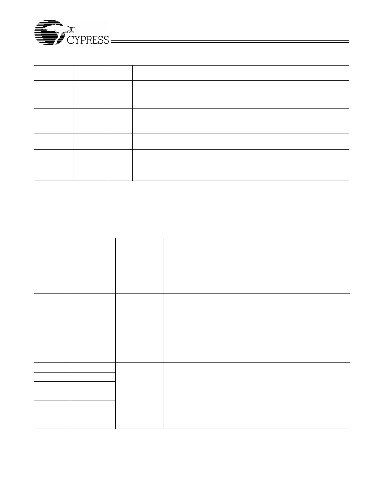
Pin Definitions
Pin Name
SDRAM0:12 2, 3, 6, 7, 10,
BUF_IN 9 I
SDATA 14 I/O
SCLOCK 15 I
VDD 1, 5, 13, 2 0,
GND 4, 8, 16, 1 7,
Pin
No.
11, 18, 19,
22, 23, 26,
27, 12
24, 28
21, 25
Type Pin Description
W40S11-23
Pin
SDRAM Outputs:
O
rising input edge to a rising output edge is 1 to 5 ns. All outpu ts are sk ew controll ed to
within ± 250 ps of each other.
Clock Input:
2
I
C Data input:
of this data sheet. In ternal 250-kΩ pull-up resistor.
2
C clock input:
I
2
the I
C section of this dat a sheet. Internal 250-kΩ pull-up resi stor.
Power Connection:
P
supply.
Ground Connection:
G
Provides buf fered copy of BUF_IN. The propagati on delay from a
This clock input has an input threshold vol tage of 1.5V (typ).
Data should be pr esen ted to thi s input as describe d in th e I
2
The I
C data clock should be present ed to this inpu t as described in
Powe r supply for core l ogic and output buff ers. Connec ted to 3.3V
Connect all ground pins to the common system ground plane.
2
C section
Functional Description
capacitiv e load . Thus , o utput s ignal ing is both TTL and CMOS
level compatible . Nominal output buffer impedance is 15Ω.
Output Drivers
The W40S11-23 output buffers are CMOS type which deliver
a rail-to-rail (GND to V
) output voltage swi ng into a nominal
DD
Operation
Data is written to the W40S11-23 in ten bytes of eight bits
each. Bytes are written in the order shown in Table 1.
Table 1. Byte Writing Sequence
Byte
Sequence Byte Name Bit Sequence Byte Description
1 Slave Address 11010010 Commands the W40S11-23 to acce pt the bits in Data Bytes 0–6 for in -
ternal register configuratio n. Since other devices may exis t on the same
common serial data b us , it is neces sary to ha v e a sp ecific sl a ve a ddre ss
for each potential receiver . The sla ve re ceiver add ress for the W40S11-23
is 11010010. Register setting wil l not be made if the Slave Addr ess is not
correct (or is for an alternate slave receiver).
2 Command
Code
Don’t Care Unused by the W40S1 1-23 , ther ef ore bi t val ues ar e igno red (don’t care).
This byte must be included i n the data write sequen ce to maintain prop er
byte allocation. The Command Code Byte is part of the standard serial
communication protocol and may be used when writi ng to another addressed slave receiver on the serial data bus.
3 Byte Count Don’t Care Unused by the W40S1 1-23 , ther ef or e bit val ues ar e i gnored (don ’t care ).
This byte must be included i n the data write sequen ce to maintain prop er
byte allocation. The Byte Count Byte is part of the standard serial communication pr otocol and may be used when writ ing to another address ed
slave receiver on the serial data bus.
4 Data Byte 0 Refer to Table 2 The data bit s in thes e bytes set int ernal W40S11-23 r egister s that co ntrol
5 Data Byte 1
6 Data Byte 2
device oper ation. The data bits are only accepted when the Address Byte
bit sequence i s 11010010, as n oted above . For description of bit control
functions, refer to Table 2, Data Byte Serial Configuration Map.
7 Data Byte 3 Don’t Care Ref er to Cypress Frequency Timing Generators.
8 Data Byte 4
9 Data Byte 5
10 Data Byte 6
2

W40S11-23
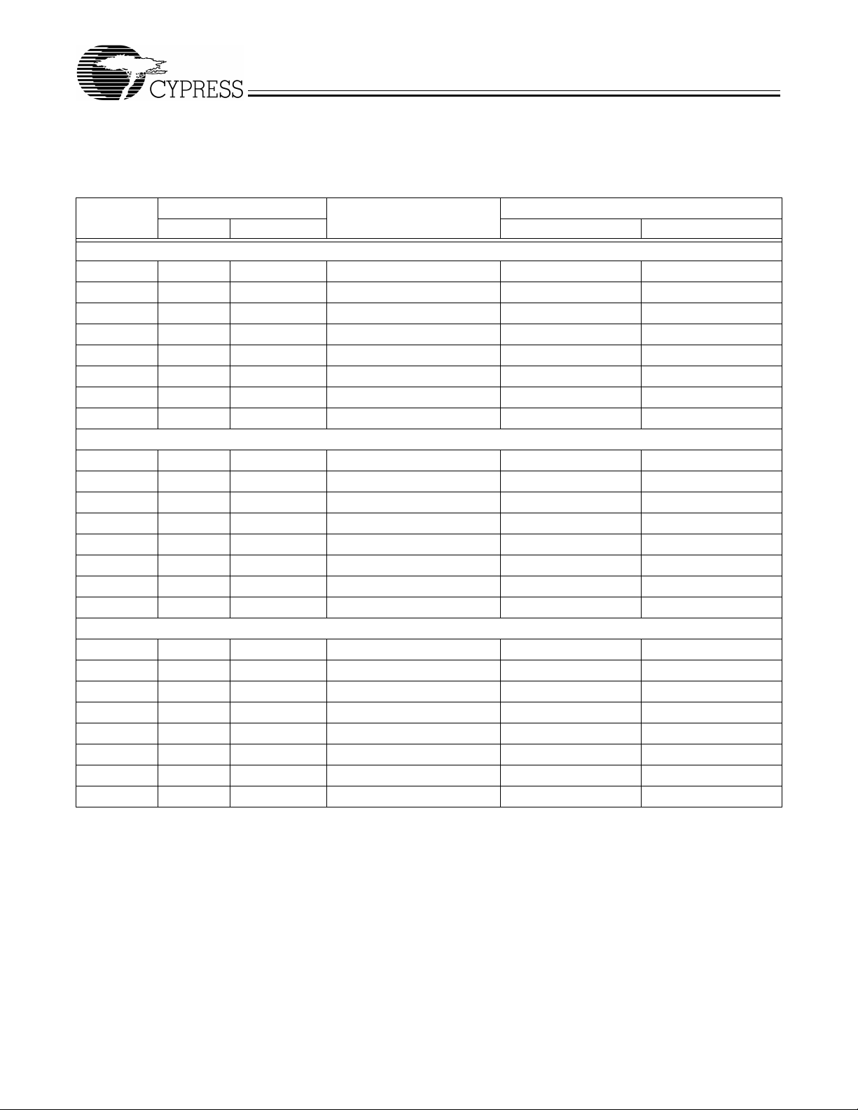
Writing Data Bytes
Each bit in the data bytes control a particular device function.
Table 2 gives the bit f ormats fo r register s located in Data Byt es
0–6.
Bits are written MSB (most significant bit) first, which is bit 7.
Table 2. Data Bytes 0–2 Serial Configuration Map
Affected Pin
Bit(s)
Pin No. Pin Name 0 1
[2]
Control Function
Bit Control
Data Byte 0 SDRAM Active/Inactive Register (1=Enable, 0=Disable)
7 11 SDRAM5 Clock Output Disable Low Active
6 10 SDRAM4 Clock Output Disable Low Active
5 N/A Reserved (Reserved) - 4 N/A Reserved (Reserved) - 3 7 SDRAM3 Clock Output Disable L ow Active
2 6 SDRAM2 Clock Output Disable L ow Active
1 3 SDRAM1 Clock Output Disable L ow Active
0 2 SDRAM0 Clock Output Disable L ow Active
Data Byte 1 SDRAM Active/Inactive Register (1=Enable, 0=Disable)
7 27 SDRAM11 Clock Output Disable Low Active
6 26 SDRAM10 Clock Output Disable Low Active
5 23 SDRAM9 Clock Output Disable Low Active
4 22 SDRAM8 Clock Output Disable Low Active
3 N/A Reserved (Reserved) - 2 N/A Reserved (Reserved) - 1 19 SDRAM7 Clock Output Disable Low Active
0 18 SDRAM6 Clock Output Disable Low Active
Data Byte 2 SDRAM Active/Inactive Register (1=Enable, 0=Disable)
7 N/A Reserved (Reserved) - 6 12 SDRAM12 Clock Output Disable Low Active
5 N/A Reserved (Reserved) -- -4 N/A Reserved (Reserved) -- -3 N/A Reserved (Reserved) -- -2 N/A Reserved (Reserved) -- -1 N/A Reserved (Reserved) -- -0 N/A Reserved (Reserved) -- --
Note:
2. At power-up all SDRAM outputs are enabled and active. Program Reserved bits to a “0.”
3
 Loading...