W40S11-02
SDRAM Buffer - 2 DIMM (Mobile)
Features
• Ten skew-controlled CMOS outputs (SDRAM0:9)
• Supports two SDRAM DIMMs
• Ideal for hi gh-performance systems designed around
Intel®’s latest Mobile chip set
2
•I
C Serial configuration interface
• Skew between any two outputs is less than 250 ps
• 1 to 5 ns propagatio n delay
• DC to 133-MHz operation
• Single 3.3V supply voltage
• Low power CMOS design pa ckaged i n a 28-pi n, 209-mil
SSOP (Shrink Small Outline Package)
Overview
The Cypress W40S11-02 is a low-voltage, ten-output clock
buffer. Output buffer impedance is approximately 15Ω, which
is ideal for driving SDRAM DIMMs.
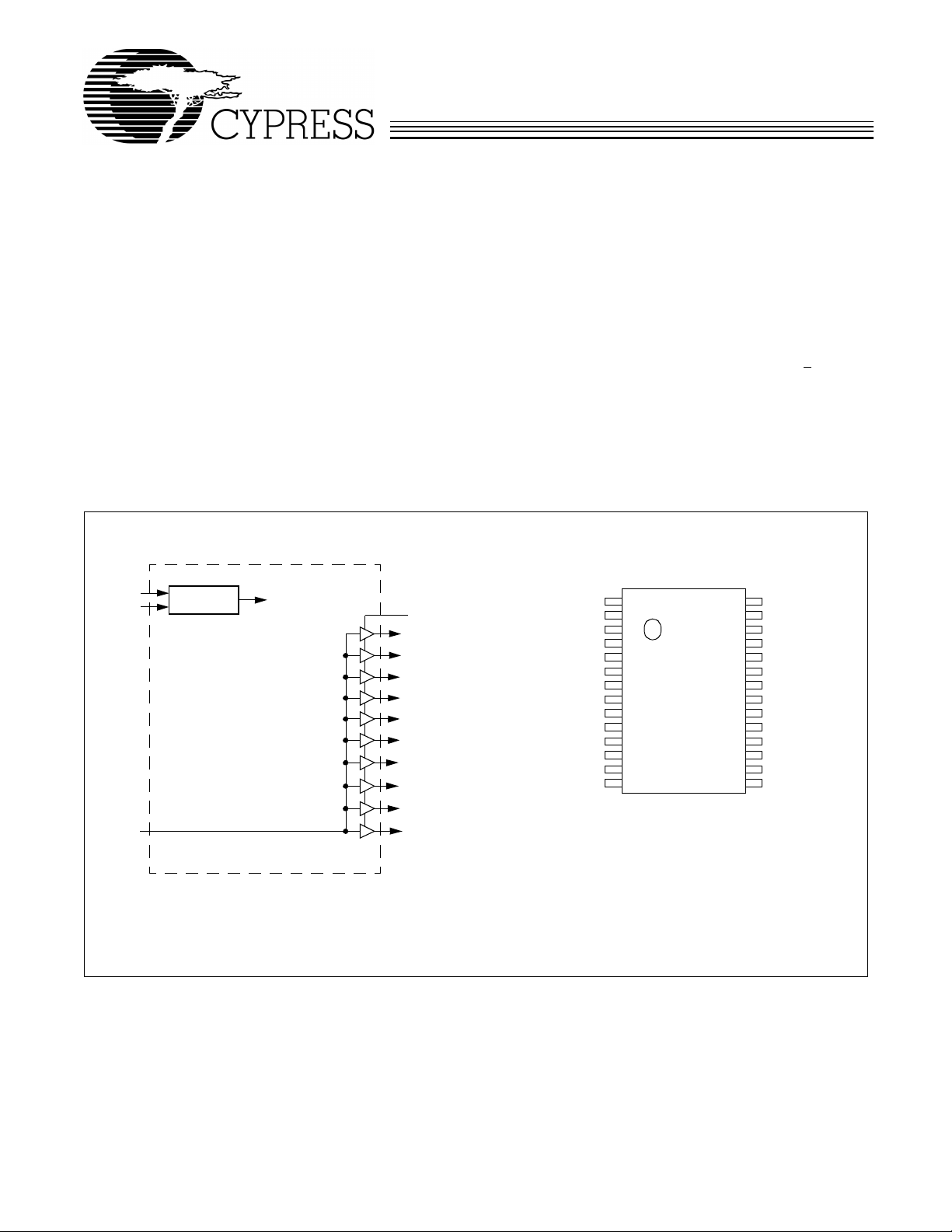
Block Diagram
SDATA
SCLOCK
BUF_IN
Serial Port
Device Control
OE
SDRAM0
SDRAM1
SDRAM2
SDRAM3
SDRAM4
SDRAM5
SDRAM6
SDRAM7
SDRAM8
SDRAM9
Key Specifications
Supply Voltages:...........................................VDD = 3.3V±5%
Operating Tempe ra tu re : .................................... 0° C to +70°C
Input Threshold: ..................................................1.5V typical
Maximu m In p ut Voltage:............. ..........................V
DD
+ 0.5V
Input Frequency:...............................................0 to 133 MHz
BUF_IN to SDRAM0:9 Propagation Delay:........1.0 to 5.0 ns
Output Edge Rate:....................... .. .. ............. .. ....... >
1.5 V/ns
Output Skew:............................................................ ±250 ps
Output Duty Cyc le : .... .. ............................ 45/5 5 % worst case
Output Impedance:...................... .. ................15 ohms typical
Output Ty pe:................................................ CMOS rail-to-rail
Pin Configuration
VDD
SDRAM0
SDRAM1
GND
VDD
SDRAM2
SDRAM3
GND
BUF_IN
VDD
SDRAM8
GND
VDD
SDATA
Note:
1. Internal pull-up resistor of 250K on SDATA, SCLOCK, and OE
inputs (should not be relied upon for pulling up to V
1
2
3
4
5
6
7
8
9
10
11
12
13
[1]
14
28
27
26
25
24
23
22
21
20
19
18
17
16
15
VDD
SDRAM7
SDRAM6
GND
VDD
SDRAM5
SDRAM4
GND
[1]
OE
VDD
SDRAM9
GND
GND
SCLOCK
DD
[1]
).
Intel is a registered trademark of Intel Corporation.
Cypress Semiconductor Corporation
• 3901 North First Street • San Jose • CA 95134 • 408-943-2600
September 29, 1999, r ev. **

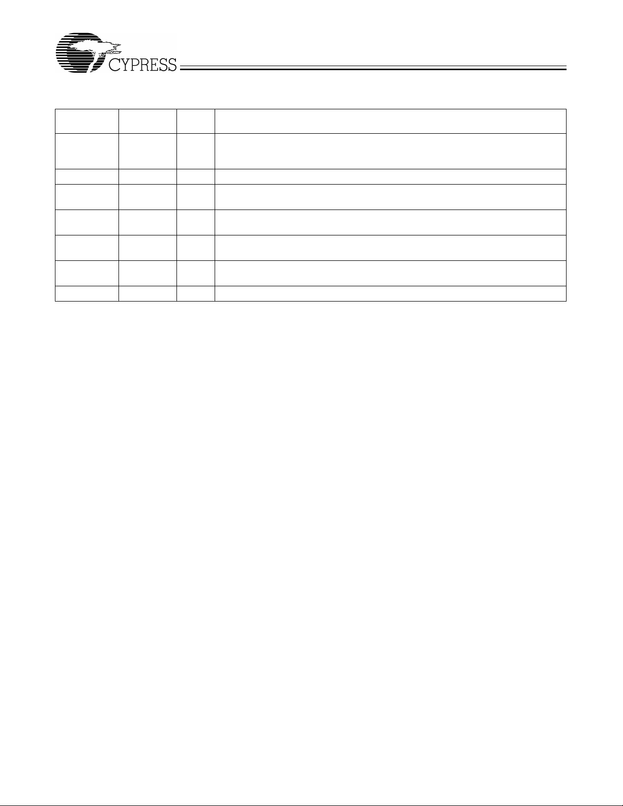
Pin Definitions
W40S11-02
Pin Name
No.
SDRAM0:9 2, 3, 6, 7,
Pin
Pin
Type Pin Description
O
22, 23, 26,
27, 11, 18
BUF_IN 9 I
SDATA 14 I/O
SCLOCK 15 I
VDD 1, 5, 10, 13,
P
19, 24, 28
GND 4, 8, 12, 16,
G
17, 21, 25
OE 20 I
SDRAM Outputs:
Provides buffered copy of BUF_IN. The propagation delay from a
rising input edge to a rising outp ut edge is 1 to 5 ns. All outputs are skew controlled
to within ± 250 ps of each other.
Clock Input:
2
C Data Input:
I
This clock inpu t has an i nput threshold voltage of 1.5V (typ).
Data should be pr esented to t his inpu t as described i n the I
2
C section
of this data sheet. Internal 250-kΩ pull-up resistor.
2
C Clock Input:
I
2
in the I
C section of this data sheet . Internal 250-kΩ pull-up resistor.
Power Connection:
2
The I
C Data clock should be presented to this input as described
Power supply for cor e logi c and output buff ers. Connected to
3.3V supply.
Ground Connection:
Output Enable:
Connect all g round pins to the common syst em ground plane.
Internal 250-kΩ pull-up resistor. Three-states out puts when LOW.
2

W40S11-02
Functional Description
Output Control Pins
Outputs three-stated when OE = 0, and toggle when OE = 1.
Outputs are in phase wit h BUF_IN b ut are pha se del a yed by 1
to 5 ns. Outputs can also be controlled via the I
Table 1. Byte Writing Sequence
Byte
Sequence Byte Name Bit Sequence Byte Description
1 Slave Address 11010010 Commands the W40S11-02 to acce pt the bits in Data Bytes 0–6 for in-
2 Command
Code
3 Byte Count Don’t Care Unused by the W40S1 1-02 , ther ef or e bit val ues ar e i gnored (don ’t care ).
4 Data Byte 0 Refer to Table 2 The data bit s in thes e bytes set int ernal W40S11-23 r egister s that co ntrol
5 Data Byte 1
6 Data Byte 2
7 Data Byte 3 Don’t Care Refer to Cypress clock drivers.
8 Data Byte 4
9 Data Byte 5
10 Data Byte 6
Don’t Care Unused by the W40S1 1-02 , ther ef ore bi t val ues ar e igno red (don’t care).
2
C interfac e.
ternal register configuration. Since other devices ma y exist on the same
common serial data b us , it is neces sary to ha v e a sp ecific sl a ve a ddre ss
for each potential receiver . The sla ve re ceiver add ress for the W40S11-02
is 11010010. Register setting wil l not be made if the Slave Addr ess is not
correct (or is for an alternate slave receiver).
This byte must be included i n the data write sequen ce to maintain prop er
byte allocation. The Command Code Byte is part of the standard serial
communication protocol and may be used when writing to another addressed slave receiver on the serial data bus.
This byte must be included i n the data write sequen ce to maintain prop er
byte allocation. The Byte Count Byte is part of the standard serial communication pr otocol and may be used when writ ing to another address ed
slave receiver on the serial data bus.
device oper ation. The data bits are only accepted when the Address Byte
bit sequence i s 11010010, as noted above. For descri pti on of bit control
functions, refer to Table 2, Data Byte Serial Configuration Map.
Output Drivers
The W40S11-02 output buffers are CMOS type which deliver
a rail-to-rail (GND to V
capacitiv e load . Thus , o utput s ignal ing is both TTL and CMOS
level compatible. Nomina l output buffer imped ance is 15 ohms.
Operation
Data is written to the W40S11-02 in ten bytes of eight bits
each. Bytes are written in the order shown in Table 1.
) output voltage sw ing into a nominal
DD
3

W40S11-02
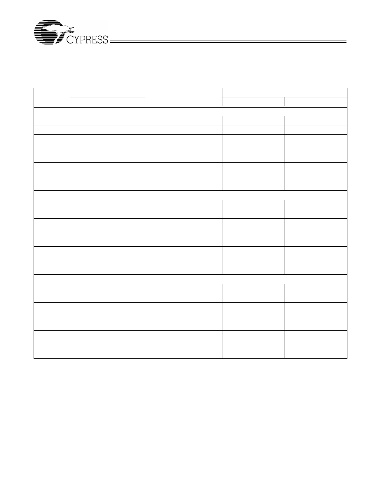
Writing Data Bytes
Each bit in the data bytes control a particular device function.
Table 2 gives the bit f ormats fo r registers lo cated in Data Byt es
0–6.
Bits are written MSB (most significant bit) first, which is bit 7.
Table 2. Data Bytes 0–2 Seri al Configuration Map
Affected Pin
Bit(s)
Pin No. Pin Name 0 1
[2]
Control Function
Bit Control
Data Byte 0 SDRAM Active/Inactive Register (1=Enable, 0=Disable)
7 N/A Reserved (Reserved) -- -6 N/A Reserved (Reserved) -- -5 N/A Reserved (Reserved) -- -4 N/A Reserved (Reserved) -- -3 7 SDRAM3 Clock Output Disable Low Active
2 6 SDRAM2 Clock Output Disable Low Active
1 3 SDRAM1 Clock Output Disable Low Active
0 2 SDRAM0 Clock Output Disable Low Active
Data Byte 1 SDRAM Active/Inactive Register (1=Enable, 0=Disable)
7 27 SDRAM7 Clock Output Disable Low Active
6 26 SDRAM6 Clock Output Disable Low Active
5 23 SDRAM5 Clock Output Disable Low Active
4 22 SDRAM4 Clock Output Disable Low Active
3 N/A Reserved (Reserved) -- -2 N/A Reserved (Reserved) -- -1 N/A Reserved (Reserved) -- -0 N/A Reserved (Reserved) -- --
Data Byte 2 SDRAM Active/Inactive Register (1=Enable, 0=Disable)
7 18 SDRAM9 Clock Output Disable Low Active
6 11 SDRAM8 Clock Output Disable Low Active
5 N/A Reserved (Reserved) -- -4 N/A Reserved (Reserved) -- -3 N/A Reserved (Reserved) -- -2 N/A Reserved (Reserved) -- -1 N/A Reserved (Reserved) -- -0 N/A Reserved (Reserved) -- --
Note:
2. At power-up all SDRAM outputs are enabled and active. It is recommended to program Bits 4–7 of Byte0 and Bits 0–3 of Byte1 to a “0” to save power and reduce
noise.
4
 Loading...