

W40S01-04
SDRAM Buffer - 4 DIMM
Features
• Eighteen skew contr ol led CMOS outputs (SDRAM0:17)
• Supports four SDRAM DIMMs
• Ideal for high-performance systems designed around
Intel®’s 440BX chip set
2
•I
C serial configuration interface
• Output skew between any two outputs is less than
250 ps
• 1 to 5 ns propagati on delay
• DC to 133-MHz operation
• Single 3.3V supply voltage
• Low power CMOS design packaged in a 48-pin SSOP
(Small Shrink Outline Package)
Overview
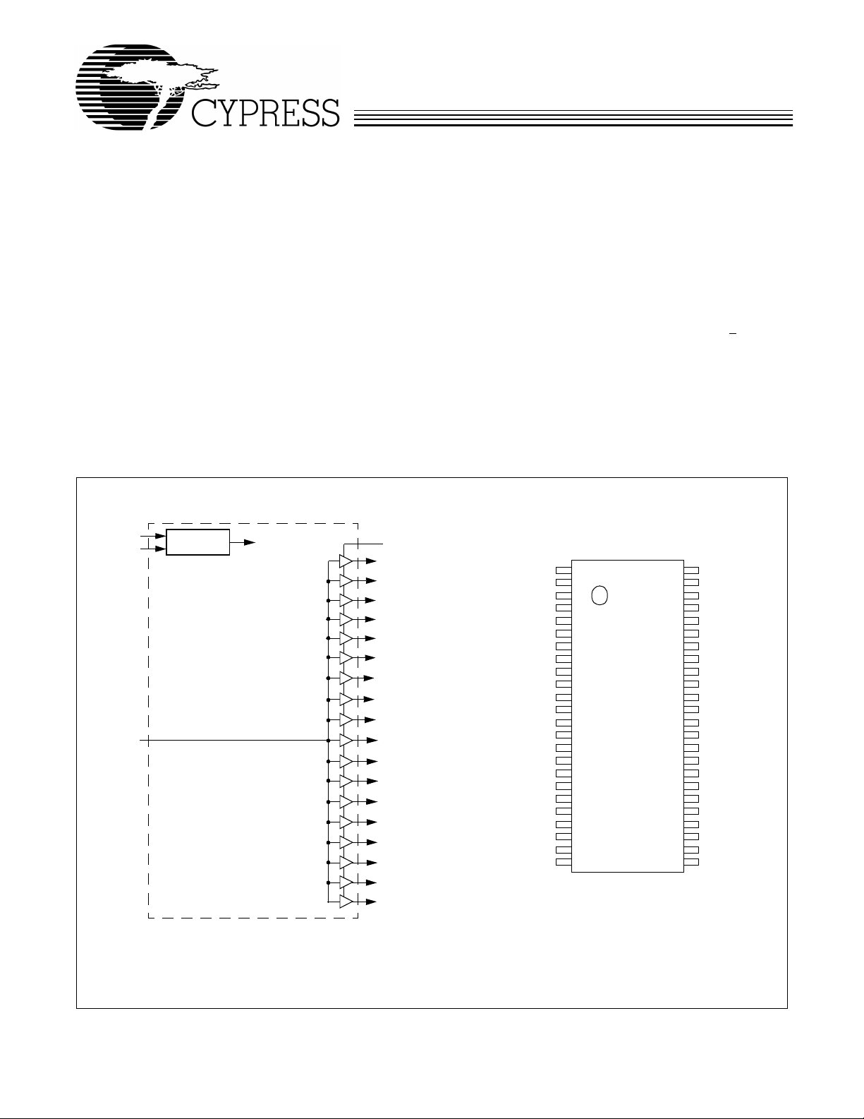
The Cypress W40S01-04 is a low-voltage, eighteen-output
signal buffer. Output buffer impedance is approximately 15
which is idea l for driving SD RA M DIM M s .
Block Diagram
SDATA
SCLOCK
BUF_IN
Serial Port
Device Control
OE
SDRAM0
SDRAM1
SDRAM2
SDRAM3
SDRAM4
SDRAM5
SDRAM6
SDRAM7
SDRAM8
SDRAM9
SDRAM10
SDRAM11
SDRAM12
SDRAM13
SDRAM14
SDRAM15
SDRAM16
SDRAM17
Key Specifications
Supply Voltages :......... .......... .. .......... .. ...... V
Operating Temperatur e:.... .. .......... .......... ......... . 0° C to +70°C
Input Threshold: .................................................. 1.5V typical
Maximum Input Voltage: ...................................V
Input Frequency:...............................................0 to 133 MHz
BUF_IN to SDRAM0:17 Propagation Del ay:......1.0 to 5.0 ns
Output Edge Rate:............................................ ......>
Output Skew:............................................................ ±250 ps
Output Duty Cycle : .... ......... .......... .. ......... 4 5 /5 5 % wo r st ca s e
Output Impedance:.................... ....................15 ohms typi cal
Output Type:................................................CMOS rail-to-rail
Part to Part Skew:........................................................700 ps
Ω
DDQ3
Pin Configuration
SSOP
NC
NC
VDDQ3
SDRAM0
SDRAM1
GND
VDDQ3
SDRAM2
SDRAM3
GND
BUF_IN
VDDQ3
SDRAM4
SDRAM5
GND
VDDQ3
SDRAM6
SDRAM7
GND
VDDQ3
SDRAM16
GND
VDDQ3
SDATA
Note:
1. Internal pull-up resistor of 250K on SDATA , SCLOCK, and OE
inputs (not CMOS level).
1
2
3
4
5
6
7
8
9
10
11
12
13
14
15
16
17
18
19
20
21
22
23
[1]
24
48
47
46
45
44
43
42
41
40
39
38
37
36
35
34
33
32
31
30
29
28
27
26
25
= 3.3V±5%
+ 0.5V
DDQ3
1.5 V/ns
NC
NC
VDDQ3
SDRAM15
SDRAM14
GND
VDDQ3
SDRAM13
SDRAM12
GND
[1]
OE
VDDQ3
SDRAM11
SDRAM10
GND
VDDQ3
SDRAM9
SDRAM8
GND
VDDQ3
SDRAM17
GND
GND
SCLOCK
[1]
Intel is a registered trademark of Intel Corporation.
Cypress Semiconductor Corporation
• 3901 North First Street • San Jose • CA 95134 • 408-943-2600
June 20, 2000, rev. **
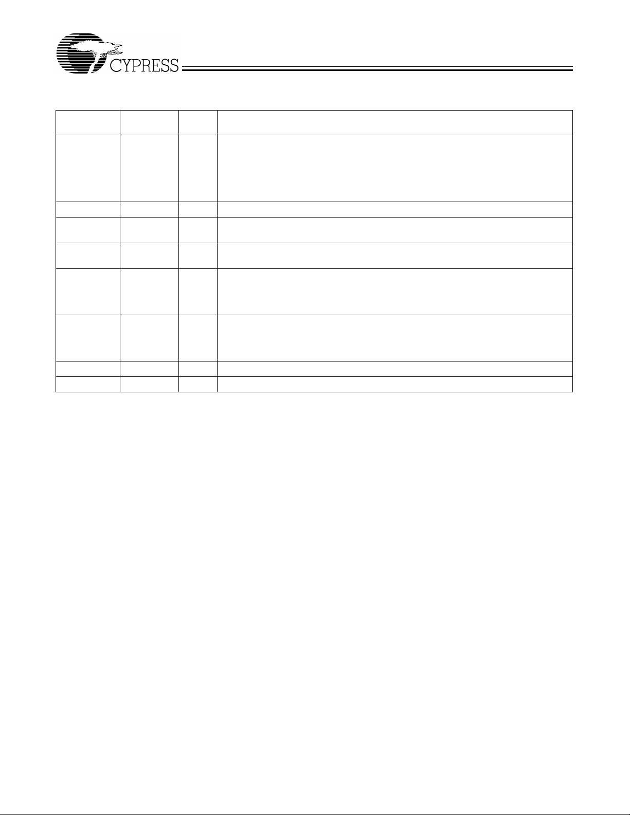
Pin Definitions
W40S01-04
Pin Name
No.
SDRAM0:17 4, 5, 8, 9,
Pin
Pin
Type Pin Description
O
13, 14, 17,
18, 21, 28,
31, 32, 35,
36, 40, 41,
44, 45
BUF_IN 11 I
SDATA 24 I/O
SCLOCK 25 I
VDDQ3 3, 7, 12, 16,
P
20, 23, 29,
33, 37, 42,
46
GND 6, 10, 15,
G
19, 22, 26,
27, 30, 34,
39, 43
OE 38 I
NC 1, 2, 47, 48 -
SDRAM Outputs:
Provides buffered copy of BUF_IN. The prop agation delay from a
rising input edge to a rising outp ut edge is 1 to 5 ns. All outputs are skew control led
to within ± 250 ps of each other.
Clock Input:
2
I
C Data Input:
This clock input has an input threshold voltage of 1.5V (typ).
Data should be pr esented to t his inpu t as described i n the I
2
C section
of this data sheet. Internal 250-kΩ pull-up resistor.
2
C clock In put:
I
2
the I
C section of this data sheet. Internal 250-kΩ pull-up resistor.
Power Connection:
2
The I
C data clock shou ld be pr ese nted to this input as de scribed in
Power supply for core logic and output buffers. Connected to
3.3V supply.
Ground Connection:
Output Enable:
No Connect:
Do not connect.
Connect all groun d pins to the common system ground plane.
Internal 250-kΩ pull-up resistor . Three-states outpu ts when LOW.
2
W40S01-04
Functional Description
Output Control Pins
Outputs three-stated when OE = 0, and toggle when OE = 1.
Outputs are in ph ase with BUF_IN but ar e phase del a yed by 1
to 5 ns. Outputs can also be controlled via the I
Output Drivers
The W40S01-04 output buffers are CMOS type which deliver
a rail-to-rail (GND to V
Table 1. Byte Writing Sequence
Byte
Sequence Byte Name Bit Sequence Byte Description
1 Slave Address 11010010 Commands the W40S01-04 t o accept t he bits in Data Byt es 0-6 for inter-
2 Command
Code
3 Byte Count Don’t Care Unused by the W40S0 1-04 , ther ef or e bit va lue s are i gnored (don ’t car e).
4 Data Byte 0 Refer to Table 2 The data bit s in thes e bytes set int ernal W40S01-04 r egister s that co ntrol
5 Data Byte 1
6 Data Byte 2
7 Data Byte 3 Don’t Care Refer to Cypress clock drivers.
8 Data Byte 4
9 Data Byte 5
10 Data Byte 6
) output voltage swing into a nominal
DD
Don’t Care Unused by the W40S0 1-04 , ther ef ore bi t va lues ar e ign ored (don’t care).
2
C interface.
nal register configuration. Since other devices may exist on the same
common serial data b us , it is neces sary to have a specific slave addr ess
for each potential receiver. The slav e receiver address for the
W40S01-04 is 11010010. Regi ster setting will not be made if t he Slave
Address is not correct (or is for an alternat e slave rece iver).
This byte must be included i n the data write sequen ce to maintain pro per
byte allocation. The Command Code Byte is part of the standard serial
communication protocol and may be used when wri ting to another addres sed slave r e ceiver on the serial da ta bus.
This byte must be included i n the data write sequen ce to maintain pro per
byte allocation. The Byte Count Byte is part of the standard serial communication pr otocol an d may be used when writ ing to another address ed
slave receiver on the serial data bus.
device oper ation. The data bits are only accepted when the Address Byte
bit sequence i s 11010010, as noted abov e. For description of bit cont rol
functio ns, refer to Table 2, Data Byte Serial Configuration Map.
capacitiv e load . Th us, o utput signal ing i s both TT L and CMOS
level compatibl e. Nominal output buff er imp edance is 15 ohms .
Operation
Data is written to the W40S01-04 in ten bytes of eight bits
each. Bytes are written in the order shown in Table 1 .
3

W40S01-04
Writing Data Bytes
Each bit in the data bytes control a particular device function.
Table 2 gives the bit f ormats f or regi st ers l ocated in Da ta Bytes
0–6.
Bits are written MSB (most significant bit) first, which is bit 7.
Table 2. Data Bytes 0–2 Serial Configuration Map
Affected Pin
Bit(s)
Pin No. Pin Name 0 1
[2]
Control Funct ion
Bit Control
Data Byte 0 SDRAM Active/Inactive Register (1=Enable, 0=Disable)
7 18 SDRAM7 Clock Output Disable Low Active
6 17 SDRAM6 Clock Output Disable Low Active
5 14 SDRAM5 Clock Output Disable Low Active
4 13 SDRAM4 Clock Output Disable Low Active
3 9 SDRAM3 Clock Output Disable L ow Active
2 8 SDRAM2 Clock Output Disable L ow Active
1 5 SDRAM1 Clock Output Disable L ow Active
0 4 SDRAM0 Clock Output Disable L ow Active
Data Byte 1 SDRAM Active/Inactive Register (1=Enable, 0=Disable)
7 45 SDRAM15 Clock Output Disable Low Active
6 44 SDRAM14 Clock Output Disable Low Active
5 41 SDRAM13 Clock Output Disable Low Active
4 40 SDRAM12 Clock Output Disable Low Active
3 36 SDRAM11 Clock Output Disable Low Active
2 35 SDRAM10 Clock Output Disable Low Active
1 32 SDRAM9 Clock Output Disable Low Active
0 31 SDRAM8 Clock Output Disable Low Active
Data Byte 2 SDRAM Active/Inactive Register (1=Enable, 0=Disable)
7 28 SDRAM17 Clock Output Disable Low Active
6 21 SDRAM16 Clock Output Disable Low Active
5 N/A Reserved (Reserved) -- -4 N/A Reserved (Reserved) -- -3 N/A Reserved (Reserved) -- -2 N/A Reserved (Reserved) -- -1 N/A Reserved (Reserved) -- -0 N/A Reserved (Reserved) -- --
Note:
2. At power-up all SDRAM outputs are enabled and active. Program Reserved bits to 0.
4

W40S01-04
How To Use the Serial Data Interface
Electrical Requirements
Figure 1 illust rat es el ectrical ch aract eristi cs for the serial interface bus used with the W40S01-04. Devices send data over
the bus with an open drain l ogic output that can (a) pull the b us
line LO W, or (b) let the b us de f ault t o log ic 1. The p ull- up resi stor on the bus (both clock and data lines) establish a default
6(5,$/ %86 '$7$ /,1(
6(5,$/ %86 &/2&. /,1(
6'&/. 6'$7$
1
'$7$ ,1
'$7$ 287
1
&/2&. ,1
&/2&. 287
logic 1. All bus devices generally have logic inputs to receive
data.
Although the W40S01-04 is a receive-only device (no data
write-back capa bil ity), it does transmi t an “acknowledge” data
pulse after each byte is received. Thus, the SDATA line can
both transmit and receive data.
The pull-up resistor should be sized to meet the rise and fall
times specif ied i n A C p aram eters , ta king i nto consi derat ion total bus line capacitance.
9'' 9''
aN
Ω
&/2&. ,1
aN
Ω
6&/2&. 6'$7$
'$7$ ,1
'$7$ 287
1
6(5,$/ %86 0$67(5 75$160,77(5
&+,3 6(7
Figure 1. Serial Interface Bus Electrical Chara cteristics
6(5,$/ %86 6/$9( 5(&(,9(5
&/2&. '(9,&(
5

W40S01-04
Sign aling R e quire m e nts
As shown in Fi gure 2, v alid dat a bits ar e defined as stable logic
0 or 1 condition on the data line during a clock HIGH (logic 1)
pulse. A trans iti oning dat a line duri ng a cloc k HIGH pulse ma y
be interpreted as a start or stop pulse (it will be interpreted as
a start or stop pulse if the start/stop timing parameters are
met).
A write sequence is i nitiat ed b y a “start bit” as sho wn i n Figure
3. A “stop bit” signifies that a transmission has ended.
As stated p re vio usly, the W40S01- 04 s ends an “acknowledge”
pulse after receiving eight data bits in each byte as shown in
Figure 4.
6'$7$
6&/2&.
9DOLG
'DWD
%LW
RI 'DWD $OORZHG
Sending Data to the W40S01-04
The device accepts data once it has detected a valid start bit
and address byte sequence. Device functionality is changed
upon the receipt of each dat a bit (registe rs are not doub le buff ered). Pa rtial transmiss ion is allo wed meaning that a transm ission can be truncated as soon as the desired data bits are
transmitt ed (remaining r egister s will be unmodified ). Transmission is truncated with either a stop bit or new start bit (restart
condition).
&KDQJH
6'$7$
6&/2&.
Figure 2. Serial Data Bus Valid Data Bit
6WDUW
%LW
Figure 3. Serial Data Bus Start and Stop Bit
6WRS
%LW
6

Figure 4. Serial Data Bus Write Sequence
Signaling from System Core Logic
Start Condition
MSB
11010010 LSB MSB MSB LSBSDATA
12345678A12345678A1234SCLOCK 12345678A
SDATA
Signaling by Clock Device
Slave Address
(First Byte)
LSB
MSB
Acknowledgment Bit
Command Code
(Second Byte)
from Clock Device
Byte Count
(Third Byte)
Last Data Byte
(Last Byte)
Stop Condition
7
Figure 5. Serial Data Bus Timing Diagram
SDATA
SCLOCK
t
STHD
t
LOW
t
t
DSU
t
HIGH
t
R
t
F
t
DHD
t
SP
t
SPSUtSTHD
t
SPSU
SPF
W40S01-04

Absolute Maximum Ratings
W40S01-04
Stresses greater than those listed in this table may cause permanent damage to the de vice . These represent a stress ratin g
only. Operation of the device at these or any other conditions
above those specified in the operati ng sections of this specification is not implied. Maximum conditions for extended periods may affect reliabil ity
Parameter Description Rating Unit
V
, V
DD
IN
T
STG
T
A
T
B
DC Electr i cal C h ar acteristi cs:
Voltage on any pin with respect to GND –0.5 to +7 .0 V
Storage Temperature –65 to +150 °C
Operating Temperature 0 to +70 °C
Ambient Temperature under Bias –55 to +125 °C
TA = 0°C to +70°C, V
DDQ3
= 3.3V±5%
T est Condition/
Parameter Description
I
DD
I
DD Tristate
3.3V Supply Current BUF_IN = 100 MHz 320 mA
3.3V Supply Current in Thr ee-state BUF_IN = 100 MHz 5 mA
Comments Min Typ Max Unit
Logic Inputs (BUF_IN, OE, SCLOCK, SDATA)
V
IL
V
IH
I
ILEAK
I
ILEAK
Logic Outputs (SDRAM0:17)
V
OL
V
OH
I
OL
I
OH
Input Low Voltage GND–0.3 0.8 V
Input High Voltage 2.0 V
Input Leakage Current, BUF_IN –5+5µA
Input Leakage Current
[4]
[3]
–20 +5 µA
Output Low Voltage IOL = 1 mA 50 mV
Output High Voltage IOH = –1 mA 3.1 V
Output Low Current VOL = 1.5V 70 110 185 mA
Output High Current VOH = 1.5V 65 100 160 mA
Pin Capacitance/Inductance
C
IN
Input Pin Capacitance (Except
BUF_IN)
C
OUT
L
IN
Notes:
3. OE, SCLOCK, and SDATA logic pins have a 250-kΩ internal pull-up resistor (not CMOS level).
4. Outputs loaded by 6" 60Ω transmission lines with 20-pF capacitors.
Output Pin Capacitance 6 pF
Input Pin Inductance 7nH
+0.5 V
DDQ3
5pF
8

W40S01-04
AC Electrical Characteristics:
TA = 0°C to +70°C, V
= 3.3V±5% (Lump Capacitance Test Load = 30 pF)
DDQ3
Parameter Description Test Condition Min Typ Max Unit
f
t
t
t
t
t
t
t
t
t
Z
T
IN
R
F
SR
SF
EN
DIS
PR
PF
D
o
SPP
Input Frequency 0 133 MHz
Output Rise Edge Rate Measured from 0.4V to 2.4 V 1.5 4.0 V/ns
Output Fall Edge Rate Measured from 2.4V to 0.4 V 1.5 4.0 V/ns
Output Skew, Rising Edges 250 ps
Output Skew, Falling Edges 250 ps
Output Enable Time 1.0 8.0 ns
Output Disable Time 1.0 8.0 ns
Rising Edge Propagation Delay 1.0 5.0 ns
Falling Edge Propagation Delay 1.0 5.0 ns
Duty Cycle Measured at 1.5V 45 55 %
AC Output Imp edance 15 Ω
Part to Part Skew 700 ps
Ordering Information
Ordering Code
Code
W40S01 04 H 48-pin SSOP (300 mils)
Document #: 38-00811
Freq. Mask
Package
Name Packag e Type
9

Package Diagram
W40S01-04
48-Pin S hr in k Sm a ll O u tline Package (S S O P, 0.300 in ch )
© Cypress Semiconductor Corporation, 1999. The information contained herein is subject to change without notice. Cypress Semiconductor Corporation assumes no responsibility for the use
of any circuitry other than circuitry embodied in a Cypress Semiconductor product. Nor does it conv ey or imply any lice nse under patent or other rights. Cypress Semicondu ctor does not authorize
its products for use as critical components in life-support systems where a malfunction or failure may reasonably be expected to result in significant injury to the user. The inclusion of Cypress
Semiconductor products in life-support systems application implies that the manufacturer assumes all risk of such use and in doing so indemnifies Cypress Semiconductor against all charges.
 Loading...