

Page 1
查询W320-04供应商
W320-04
200-MHz Spread Spectrum Clock Synthesizer/Driver
with Differential CPU Outputs
2W320-04
• Compliant with Intel
specifications
• Multiple output clocks at different frequencies
—Three pairs of differential CPU outputs, up to 2 00 MHz
—Ten synchronous PCI clocks, three free-running
—Six 3V66 clocks
—Two 48-MHz clocks
—One reference clock at 14.318 MHz
—One VCH clock
• Spread Spectrum clocking (down spread) Enables reduction of electromagnetic interference (EMI)
• Power-down features (PCI_STOP#, CPU_STOP#
PWR_DWN#)
• Three Select inputs (Mode select and IC Frequency
Select)
• OE and Test Mode support Enables ATE and “bed of nails” testing
• 56-pin SSOP package and 56-pin TSSOP package Widely available standard package enables lower cost
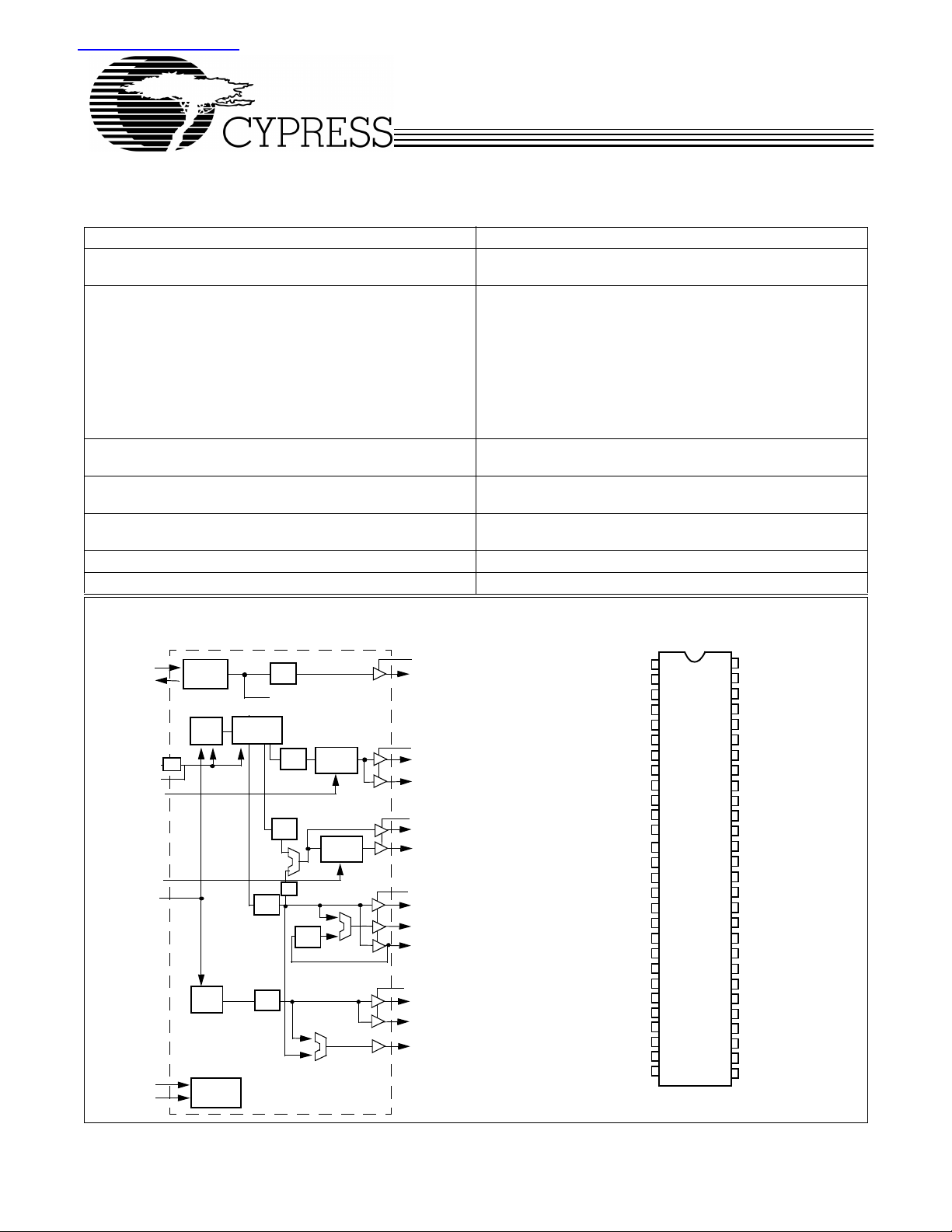
Logic Block Diagram
X1
X2
S0:2
PWR_GD#
CPU_STOP#
PCI_STOP#
PWR_DWN#
SDATA
SCLK
Gate
XTAL
OSC
PLL 1
PLL 2
SMBus
Logic
Features Benefits
®
CK-Titan clock synthesizer/driver
Supports next-generation Pentium® processors using
differential clock drivers
Motherboard clock generator
—Supports multiple CPUs and a chipset
—Support for PCI slots and chipset
—Supports AGP, DRCG reference, and Hub Link
—Supports USB host controller and graphic controller
—Supports ISA slots and I/O chip
and overall system cost
Enables ACPI-compliant designs
Supports up to four CPU clock frequencies
Pin Configurations
SSOP and TSSOP
PWR
PLL Ref Freq
Divider
Network
PWR
PWR
PWR
PWR
VDD_REF
REF
Stop
Clock
Control
Stop
Clock
Control
/2
PWR
VDD_CPU
CPU0:2
CPU#0:2
VDD_PCI
PCI_F0:2
PCI0:6
VDD_3V66
3V66_0
3V66_2:4/
66BUFF0:2
3V66_5/ 66IN
VDD_48MHz
USB (48MHz)
DOT (48MHz)
VCH_CLK/ 3V66_1
VDD_REF
XTAL_IN
XTAL_OUT
GND_REF
PCI_F0
PCI_F1
PCI_F2
VDD_PCI
GND_PCI
PCI0
PCI1
PCI2
PCI3
VDD_PCI
GND_PCI
PCI4
PCI5
PCI6
VDD_3V66
GND_3V66
66BUFF0/3V66_2
66BUFF1/3V66_3
66BUFF2/3V66_4
66IN/3V66_5
PWR_DWN#
VDD_CORE
GND_CORE
PWR_GD#
Top View
1
2
3
4
5
6
7
8
9
10
11
12
13
14
15
16
17
18
19
20
21
22
23
24
25
26
27
28
W320-04
56
55
54
53
52
51
50
49
48
47
46
45
44
43
42
41
40
39
38
37
36
35
34
33
32
31
30
29
REF
S1
S0
CPU_STOP#
CPU0
CPU#0
VDD_CPU
CPU1
CPU#1
GND_CPU
VDD_CPU
CPU2
CPU#2
MULT0#
IREF
GND_IREF
S2
USB
DOT
VDD_ 48 MHz
GND_ 48 MHz
3V66_1/VCH
PCI_STOP#
3V66_0
VDD_3V66
GND_3V66
SCLK
SDATA
Cypress Semiconductor Corporation • 3901 North First Street • San Jose • CA 95134 • 408-943-2600
Document #: 38-07010 Rev. *B Revised January 8, 2002
Page 2
W320-04
Pin Summary
Name Pins Description
REF 56 3.3V 14.318-MHz clock output.
XTAL_IN 2 14.318-MHz crystal input.
XTAL_OUT 3 14.318-MHz crystal input.
CPU, CPU# [0:2] 44, 45, 48, 49, 51, 52 Differential CPU clock outputs.
3V66_0 33 3.3V 66-MHz clock output.
3V66_1/VCH 35 3.3V selectable through SMBus to be 66 MHz or 48 MHz.
66IN/3V66_5 24 66-MHz input to buffered 66BUFF and PCI or 66-MHz clock from
66BUFF [2:0] /3V66 [4:2] 21, 22, 23 66-MHz buffered outputs from 66In put or 66-MHz clocks from internal
PCI_F [0:2] 5, 6, 7, 33-MHz clocks d ivided down from 6 6Input or divided down from 3V66.
PCI [0:6] 10, 11, 12, 13, 16, 17, 18 PCI clock outputs divided down from 66Input or divided down from
USB 39 Fixed 48-MHz clock output.
DOT 38 Fixed 48-MHz clock output.
S2 40 Special 3.3V 3-level input for Mode selection.
S1, S0 54, 55 3.3V LVTTL inputs for CPU frequency selection.
IREF 42 A precision resis tor is at tac hed to th is pi n, w hic h is c on nec ted to th e
MULT0 43 3.3V LVTTL input for selecting the current multiplier for the CPU
PWR_DWN# 25 3.3V LVTTL input for Power_Down# (active LOW).
PCI_STOP# 34 3.3V LVTTL input for PCI_STOP# (active LOW).
CPU_STOP# 53 3.3V LVTTL input for CPU_STOP# (active LOW).
PWRGD# 28 3.3V L VTTL i nput i s a lev el se nsiti ve str obe us ed to d eter mine wh en
SDATA 29 SMBus compatible SDATA.
SCLK 30 SMBus compatible SCLK.
VDD_REF, VDD_PCI,
VDD_3V66, VDD_CPU
VDD_48 MHz 37 3.3V power supply for 48 MHz.
VDD_CORE 26 3.3V power supply for PLL.
GND_REF, GND_PCI,
GND_3V66, GND_IREF,
VDD_CPU
GND_CORE 27 Ground for PLL.
1, 8, 14, 19, 32, 46, 50 3.3V power supply for outputs.
4, 9, 15, 20, 31, 36 , 41, 47 Ground for outputs.
internal VCO.
VCO.
3V66.
internal current reference.
outputs.
S[2:0] and MULTI0 inputs are valid and OK to be sampled (Active
LOW). Once PWRGD# i s sampled LOW, the status of this output wi ll
be ignored.
Document #: 38-07010 Rev. *B Page 2 of 18
Page 3
W320-04
Function Table
[1]
66BUFF[0:2]/
S2 S1 S0
CPU
(MHz)
3V66[0:1]
(MHz)
3V66[2:4]
(MHz)
66IN/3V66_5
(MHz)
PCI_F/PCI
(MHz) REF0(MHz)
USB/DOT
(MHz) Notes:
1 0 0 66 MHz 66 MHz 66IN 66 MHz Input 66IN/2 14.318 MHz 48 MHz 2, 3, 4
1 0 1 100 MHz 66 MHz 66IN 66 MHz Input 66IN/2 14.318 MHz 48 MHz 2, 3, 4
1 1 0 200 MHz 66 MHz 66IN 66 MHz Input 66IN/2 14.318 MHz 48 MHz 2, 3, 4
1 1 1 133 MHz 66 MHz 66IN 66 MHz Input 66IN/2 14.318 MHz 48 MHz 2, 3, 4
0 0 0 66 MHz 66 MHz 66 MHz 66 MHz 33 MHz 14.318 MHz 48 MHz 2, 3, 4
0 0 1 100 MHz 66 MHz 66 MHz 66 MHz 33 MHz 14.318 MHz 48 MHz 2, 3, 4
0 1 0 200 MHz 66 MHz 66 MHz 66 MHz 33 MHz 14.318 MHz 48 MHz 2, 3, 4
0 1 1 133 MHz 66 MHz 66 MHz 66 MHz 33 MHz 14.318 MHz 48 MHz 2, 3, 4
Mid 0 0 Hi-Z Hi-Z Hi-Z Hi-Z Hi-Z Hi-Z Hi-Z 1, 5
Mid 0 1 TCLK/2 TCLK/4 TCLK/4 TCLK/4 TCLK/8 TCLK TCLK/2 7, 8, 5
Mid 1 0 Reserved Reserved Reserved Reserved Reserved Reserved Reserved –
Mid 1 1 Reserved Reserved Reserved Reserved Reserved Reserved Reserved –
Swing Select Functions
Mult0 Board Target Trace/Term Z Reference R, IREF
050Ω Rr = 221 1%, IREF = 5.00 mA I
150Ω Rr = 475 1%, IREF = 2.32 mA I
/(3*Rr) Output Current VOH @ Z
= VDD
= 4*IREF 1.0V @ 50
OH
= 6*IREF 0.7V @ 50
OH
Clock Driver Impedances
Impedance
Buffer Name V
Range Buffer Type Min. Ω Typ. Ω Max. Ω
DD
CPU, CPU# Type X1 50
REF 3.135–3.465 Type 5 12 30 55
PCI, 3V66, 66BUFF 3.135–3.465 Type 5 12 30 55
USB 3.135–3.465 Type 3A 12 30 60
DOT 3.135–3.465 Type 3B 12 30 60
Clock Enable Configuration
PWR_DWN# CPU_STOP# PCI_STOP# CPU CPU# 3V66 66BUFF PCI_F PCI USB/DOT
0 X X IREF*2 FLOAT LOW LOW LOW LOW LOW OFF
1 0 0 ON FLOAT ON ON ON OFF ON ON
1 0 1 ON LOW ON ON ON ON ON ON
1 1 0 ONONONONONOFFON ON
1 1 1 ONONONONONONON ON
Note:
1. TCLK is a test clock driven in on the XTALIN input in test mode.
2. “Normal” mode of operation
3. Range of reference frequency allowed is min. = 14.316, nom. = 14.31818 MHz, max. = 14.32 MHz.
4. Frequency accuracy of 48 MHz must be +167PPM to match USB default.
5. Mid. is defined a Voltage level between 1.0V and 1.8V for three-level input functionality. Low is below 0.8V. High is above 2.0V.
6. Required for DC output impedance verification.
7. These modes are to use the SAME internal dividers as the CPU = 200 MHz mode. The only change is to slow down the internal VCO to allow under clock
margining.
VCOS/
OSC
Document #: 38-07010 Rev. *B Page 3 of 18
Page 4
W320-04
Serial Data Interface (SMBus)
T o e nhance the fl exibility a nd function o f the clock synthesize r ,
a two signal SMBus i nterfac e is prov ided ac cording to SMBu s
specification. Through the Serial Data Interface, various
device functions such as individual clock output buffers, can
be individually enabled or disabled. W320-04 support both
block read and block write operati ons .
The registers associated with the Serial Data Interface
initialize to their default setting upon power-up, and therefore
use of this interface i s optional. Cl ock devi ce register changes
are normally made upon system initialization, if any are
required. The interface can also be used during system
operation for power management functions.
Data Protocol
The clock driver s eri al protocol accepts only block writ es from
the controller . The bytes must be accessed i n sequential order
from lowest to highest byte, (most significant bit first) with the
Start
Slave Address
bit
1 1 0 1 0 0 1 0
1 bit 7 bits 1 1 8 bits 1 8 bits 1 8 bits 1 8 bits 1 1 bit
From Master to Slave
From Slave to Master
R/W 0/1 A Command
Code
0 0 0 0 0 0 0 0
Figure 1. An Example of a Block Write
AByte Count = NAData Byte 0A . . . Data Byte N-1 AStop
ability to stop after any complete byte has been transferred.
Indexed bytes are not allowed.
A block write begins with a slave address and a WRITE
condition. The R/W bit is used by the SMBus controller as a
data direction bit. A zero indicates a WRITE condition to the
clock device. The slave receiver address is 11010010 (D2h).
A command code of 0000 00 00 (00h) and the byte count byte s
are required for any transfer. After the command code, the
core logic issues a byte count which describes number of
additional bytes required for the transfer, not including the
command code and byte cou nt bytes. For exa mple, if the hos t
has 20 data bytes to send, the first byte w oul d be the numb er
20 (14h), followed by the 20 bytes o f data. The byte count byte
is required to be a minimum of 1 byte and a maximum of 32
bytes It may not be 0. Figure 1 shows an example of a block
write.
A transfer is considered val id a fter th e ac k nowl edge bit corresponding to the byte count is read by the controller.
bit
Data Byte Configuration Map
Data Byte 0: Control Register (0 = Enable, 1 = Disable)
Bit
Bit 7 5, 6, 7, 10,
Bit 6 – TBD TBD R 0
Bit 5 35 3V66_1/VCH VCH Select 66 MHz/48 MHz
Bit 4 44, 45, 48,
Bit 3 10, 1 1, 12,
Bit 2 –– S2
Bit 1 –– S1
Bit 0 –– S0
Affected
Pin# Name Description Type
11, 12, 13,
16, 17, 18,
33, 35
49, 51, 52
13, 16, 17,
18
PCI [0:6]
CPU[2:0]
3V66[1:0]
CPU [2:0]
CPU# [2:0]
PCI [6:0] PCI_STOP#
Spread Spectrum Enable
0 = Spread Off, 1 = Spread On
0 = 66 MHz, 1 = 48 MHz
CPU_STOP#
Reflects the current value of the external CPU_STOP# pin
(Does not affect PCI_F [2:0] pins)
Reflects the value of the S2 pin sampled on power-up
Reflects the value of the S1 pin sampled on power-up
Reflects the value of the S1 pin sampled on power-up
R/W 0
R/W 0
RN/A
R/W N/A
RN/A
RN/A
RN/A
Power On
Default
Document #: 38-07010 Rev. *B Page 4 of 18
Page 5
W320-04
Data Byte 1
Bit Pin# Name Description Type
Bit 7 – N/A CPU Mult0 Value R N/A
Bit 6 52, 49, 45CPU0:2 Three-State CPU0:2 during power down
R/W 0
0 = Normal; 1 = Three-stated
Bit 5 44, 45 CPU2
CPU2#
Bit 4 48, 49 CPU1
CPU1#
Bit 3 51, 52 CPU0
CPU0#
Bit 2 44, 45 CPU2
CPU2#
Bit 1 48, 49 CPU1
CPU1#
Bit 0 51, 52 CPU0
CPU0#
Allow Control of CPU2 with assertion of CPU_ST OP#
0 = Not free running; 1 = Free running
Allow Control of CPU1 with assertion of CPU_ST OP#
0 = Not free running;1 = Free running
Allow Control of CPU0 with assertion of CPU_ST OP#
0= Not free running; 1 = Free running
CPU2 Output Enable
1 = Enabled; 0 = Disabled
CPU1Output Enable
1 = Enabled; 0= Disabled
CPU0 Output Enable
1 = Enabled; 0 = Disabled
R/W 0
R/W 0
R/W 0
R/W 1
R/W 1
R/W 1
Data Byte 2
Bit Pin# Name Pin Description Type
Bit 7 – N/A N/A R 0
Bit 6 18 PCI6 PCI6 Output Enable
R/W 1
1 = Enabled; 0 = Disabled
Bit 5 17 PCI5 PCI5 Output Enable
R/W 1
1 = Enabled; 0 = Disabled
Bit 4 16 PCI4 PCI4 Output Enable
R/W 1
1 = Enabled; 0 = Disabled
Bit 3 13 PCI3 PCI3 Output Enable
R/W 1
1 = Enabled; 0 = Disabled
Bit 2 12 PCI2 PCI2 Output Enable
R/W 1
1 = Enabled; 0 = Disabled
Bit 1 11 PCI1 PCI1 Output Enable
R/W 1
1 = Enabled; 0 = Disabled
Bit 0 10 PCI0 PCI0 Output Enable
R/W 1
1 = Enabled; 0 = Disabled
Power On
Default
Power On
Default
Data Byte 3
Power On
Bit Pin# Name Pin Description Type
Default
Bit 7 38 DOT DOT 48-MHz Output Enable R/W 1
Bit 6 39 USB USB 48-MHz Output Enable R/W 1
Bit 5 7 PCI_F2 Allow control of PCI_F2 with assertion of PCI_STOP#
R/W 0
0 = Free running; 1 = Stopped with PCI_STOP#
Bit 4 6 PCI_F1 Allow control of PCI_F1 with assertion of PCI_STOP#
R/W 0
0 = Free running; 1 = Stopped with PCI_STOP#
Bit 3 5 PCI_F0 Allow control of PCI_F0 with assertion of PCI_STOP#
R/W 0
0 = Free running; 1 = Stopped with PCI_STOP#
Bit 2 7 PCI_F2 PCI_F2 Outpu t Enable R/W 1
Bit 1 6 PCI_F1 PCI_F1Output Enable R/W 1
Bit 0 5 PCI_F0 PCI_F0 Outpu t Enable R/W 1
Document #: 38-07010 Rev. *B Page 5 of 18
Page 6
W320-04
Data Byte 4
Bit Pin# Name Pin Description Type
Bit 7 – TBD N/A R 0
Bit 6 – TBD N/A R 0
Bit 5 33 3V66_0 3V66_0 Output Enable
1 = Enabled; 0 = Disabled
Bit 4 35 3V66_1/VCH 3V66_1/VCH Output Enable
1 = Enabled; 0 = Disabled
Bit 3 24 66IN/3V66_5 3V66_5 Output Enable
1 = Enable; 0 = Disable
NOTE: This bit should be used when pin 24 is confi gured
as 3v66_5 output. Do not clear this bit when pin 24 is
configured as 66in input.
Bit 2 23 66BUFF2 66-MHz Buffered 2 Output Enable
1 = Enabled; 0 = Disabled
Bit 1 22 66BUFF1 66-MHz Buffered 1 Output Enable
1 = Enabled; 0 = Disabled
Bit 0 21 66BUFF0 66-MHz Buffered 0 Output Enable
1 = Enabled; 0 = Disabled
Data Byte 5
Bit Pin# Name Pin Description Type
Bit 7 N /A N/A R 0
Bit 6 N /A N/A R 0
Bit 5 66BUFF [2:0] Tpd 66IN to 66BUFF propagation delay control R/W 0
Bit 4 66BUF F [2:0] R/W 0
Bit 3 DOT DOT edge rate control R/W 0
Bit 2 D OT R/W 0
Bit 1 U SB USB edge rate control R/W 0
Bit 0 USB R/W 0
R/W 1
R/W 1
R/W 1
R/W 1
R/W 1
R/W 1
Power On
Default
Power On
Default
Byte 6: Vendor ID
Bit Description Type Power On Default
Bit 7 Revision Code Bit 3 R 0
Bit 6 Revision Code Bit 2 R 0
Bit 5 Revision Code Bit 1 R 0
Bit 4 Revision Code Bit 0 R 0
Bit 3 Vendor ID Bit 3 R 1
Bit 2 Vendor ID Bit 2 R 0
Bit 1 Vendor ID Bit 1 R 0
Bit 0 Vendor ID Bit 0 R 0
Document #: 38-07010 Rev. *B Page 6 of 18
Page 7
W320-04
Maximum Ratings
(Above which the useful life may be impaired. For user g uid elines, not tested.)
Supply Voltage..................................................–0.5 to +7.0V
Input Voltage..............................................–0.5V to V
Operating Conditions
[8]
Over which Electrical Parameters are Guaranteed
DD
+0.5
Storage Temperature (Non-Condensing) ... –65°C to +150°C
Max. Soldering Temperature (10 sec)...................... +260°C
Junction Temperature............................................... +150°C
Package Power Dissipation...............................................1Ω
Static Discharge Voltage
(per MIL-STD-883, Method 3015)............................> 2000V
Parameter Description Min. Max. Unit
V
V
V
T
C
C
C
f
(REF)
, V
DD_REF
DD_3V66, VDD_CPU,
DD_48 MHz
A
in
XTAL
L
DD_PCI,VDD_CORE
,
3.3V Supply Voltages 3.135 3.465 V
48-MHz Supply Voltage 2.85 3.465 V
Operating Temperature, Ambient 0 70 °C
Input Pin Capacitance 5 pF
XTAL Pin Capacitance 22.5 pF
Max. Capacitive Load on
USBCLK, REF
PCICLK, 3V66
20
30
Reference Frequency, Oscillator Nominal Value 14.318 14.318 MHz
pF
Electrical Characteristics Ov er the Op erat ing Range
Parameter Description Test Conditions Min. Max. Unit
V
IH
V
IL
V
OH
V
OL
I
IH
I
IL
I
OH
I
OL
I
OZ
I
DD3
I
DDPD3
I
DDPD3
Note:Notes:
8. The voltage on any input or I/O pin cannot exceed te powe pin during power-ujp. Power supply sequencing is NOT required.
High-level Input Voltage Except Crystal Pads. Threshold Voltage for Crystal Pads = VDD/2 2.0 V
Low-level Input Voltage Except Crystal Pads 0.8 V
High-level Output Voltage USB, REF, 3V66 IOH = –1 mA 2.4 V
PCI I
= –1 mA 2.4 V
OH
Low-level Output Voltage USB, REF, 3V66 IOL = 1 mA 0.4 V
PCI I
Input HIGH Current 0 < VIN < V
Input LOW Current 0 < VIN < V
High-level Output Current CPU
For IOH =6*IRef Configuration
REF, DOT, USB Type 3, V
3V66, DOT, PCI, REF Type 5, V
DD
DD
= 1 mA 0.55 V
OL
–55mA
–55mA
Type X1, VOH = 0.65V 12.9 mA
Type X1, V
Type 3, V
= 0.74V 14.9
OH
= 1.00V –29
OH
= 3.135V –23
OH
= 1.00V –33
OH
Type 5, VOH = 3.135V –33
Low-level Output Current REF, DOT, USB Type 3, VOL = 1.95V 29 mA
Type 3, V
3V66, PCI, REF Type 5, V
Type 5, V
= 0.4V 27
OL
=1.95 V 30
OL
= 0.4V 38
OL
Output Leakage Current Three-state 10 mA
3.3V Power Supply Current VDD_CORE/VDD3.3 = 3.465V, F
= 133 MHz 360 mA
CPU
3.3V Shut-down Current VDD_CORE/VDD3.3 = 3.465V and @ IREF = 2.32 mA 25 mA
3.3V Shut-down Current VDD_CORE/VDD3.3 = 3.465V and @ IREF = 5.0 mA 45 mA
Document #: 38-07010 Rev. *B Page 7 of 18
Page 8

W320-04
-
Switching Characteristics
[9]
Over the Operating Range
Parameter Output Description Test Conditions Min. Max. Unit
t
1
t
3
t
3
t
5
t
5
t
6
t
7
t
9
t
9
t
9
t
9
All Output Duty Cycle
USB, REF,
Falling Edge Rate Between 2.4V and 0.4V 0.5 2.0 ns
DOT
PCI,3V66 Falling Edge Rate Between 2.4V and 0.4V 1.0 4.0 V/ns
3V66[0:1] 3V66-3V66 Skew Measured at 1.5V 500 ps
66BUFF[0:2] 66BUFF-66BUFF Skew Measured at 1.5V 175 ps
PCI PCI-PCI Skew Measured at 1.5V 500 ps
3V66, PCI 3V66-PCI Cloc k Jitter 3V66 leads. Measured at 1.5V 1.5 3.5 ns
3V66 Cycle-Cycle Clock Jitter Measured at 1.5V t
USB, DOT Cycle-Cycle Clock Jitter Measured at 1.5V t
PCI Cycle-Cycle Clock Jitter Measured at 1.5V t
REF Cycle-Cycle Clock Jitter Measured at 1.5V t
[10]
Measured at 1.5V 45 55 %
9 = t9A
9 = t9A
9 = t9A
9 = t9A
– t
– t
– t
– t
9B
9B
9B
9B
250 ps
350 ps
500 ps
1000 ps
CPU 1.0V Switching Characteristics
t
2
t
3
t
4
t
8
Voh CPU High-level Output Voltage
CPU Rise Time Measured differential waveform from
175 467 ps
–0.35V to +0.35V
CPU Fall Time Measured differential waveform from
175 467 ps
–0.35V to +0.35V
CPU CPU-CPU Skew Measured at Crossover 150 ps
CPU Cycle-Cycle Clock Jitter Measured at Crossover t
CPU Rise/Fall Matching Measured with test loads
Measured with test loads
8 = t8A
[13]
[12]
– t
8B
0.92 1.45 V
150 ps
325 mV
including overshoot
Vol CPU Low-level Output Voltage
Measured with test loads
[12]
–0.2 0.35 V
including undershoot
V
crossover
CPU Crossover Voltage Measured with test loads
[12]
0.51 0.76 V
CPU 0.7V Switching Characteristics
t
2
t
3
t
4
t
8
Voh CPU High-level Output Voltage
CPU Rise Time Measured single ended waveform
175 700 ps
from 0.175V to 0.525V
CPU Fall Time Measured single ended waveform
175 700 ps
from 0.175V to 0.525V
CPU CPU-CPU Skew Measured at Crossover 150 ps
CPU Cycle-Cycle Clock Jitter Measured at Crossover t
With all outputs running
CPU Rise/Fall Matching Measured with test loads
Measured with test loads
8 = t8A
[11, 12]
[12]
– t
8B
150 ps
20 %
0.85 V
Including Oversho ot
Vol CPU Low-level Output Voltage
Measured with test loads
[12]
–0.15 V
Including Undershoot
V
crossover
Notes:
9. All parameters specified with loaded outputs.
10. Duty cycle is measured at 1.5V when V
11. Determined as a fraction of 2*(Trp – Trn)/(Trp +Trn) Where Trp is a rising edge and Trp is an intersecting falling edge.
12. The 0.7V test load is R
13. The 1.0V test load is shown on the test circuit page.
CPU Crossover Voltage Measured with test loads
= 3.3V. When VDD = 2.5V, duty cycle is measured at 1.25V.
DD
= 33.2 ohm, Rp = 49.9 ohm in test circuit.
s
[12]
0.28 0.43 V
Document #: 38-07010 Rev. *B Page 8 of 18
Page 9

Definition and Application of PWRGD# Signal
Vtt
W320-04
VRM8.5
PWRGD#
3.3V
NPN
CPU
BSEL0
3.3V 3.3V
BSEL1
PWRGD#
CLOCK
GENERATOR
S0
S1
10K
10K
10K
GMCH
10K
Document #: 38-07010 Rev. *B Page 9 of 18
Page 10

Switching Waveforms
W320-04
Duty Cycle Timing
(Single-ended Output)
t
1B
t
1A
Duty Cycle Timing (CPU Differential Output)
t
1B
t
1A
All Outputs Rise/Fall Time
OUTPUT
t
2
CPU-CPU Clock Skew
V
DD
t
3
0V
Host_b
Host
Host_b
Host
3V66-3V66 Clock Skew
3V66
3V66
PCI-PCI Clock Skew
PCI
PCI
t
4
Document #: 38-07010 Rev. *B Page 10 of 18
Page 11

Switching Waveforms (continued)
3V66-PCI Clock Skew
3V66
PCI
t
7
CPU Clock Cycle-Cycle Jitter
W320-04
Host_b
Host
Cycle-Cycle Clock Jitter
CLK
PWRDWN# Assertion
66BUFF
PCI
PCI_F (APIC)
t
8A
t
9A
t
8B
t
9B
Power Down Rest of Generator
PWR_DWN#
CPU
CPU#
3V66
66IN
USB
REF
Note: PCI_STOP# asserted LOW
UNDEF
Document #: 38-07010 Rev. *B Page 11 of 18
Page 12

PWRDWN# Deassertion
66BUFF1/GMCH
66BUFF0,2
PCI
PCI_F (APIC)
PWR_DWN#
CPU
CPU#
3V66
66IN
USB
REF
< 3 ms
W320-04
10-30 µs min.
100-200 µs max.
Note: PCI_STOP# asserted LOW
PWRGD# Timing Diagrams
GND VRM 5/12V
PWRGD#
VID [3:0]
BSEL [1:0]
PWRGD# FROM
PWRGD# FROM
VCC CPU CORE
VCC W320 CLOCK
GEN
CLOCK OUTPUTS
VRM
NPN
PWRGD#
CLOCK STATE
CLOCK VCO
State 0
OFF
OFF
Possible glitch while Clock VCC is coming
up. Will be gone in 0.2–0.3 mS delay.
0.2 -- 0.3 ms
Wait for
PWRGD#
Sample
BSELS
delay
State 1 State 2 State 3
Figure 2. CPU Power Before Clock Power
ON
ON
Document #: 38-07010 Rev. *B Page 12 of 18
Page 13

GND VRM 5/12V
PWRGD#
VID [3:0]
BSEL [1:0]
PWRGD# FROM
PWRGD# FROM
VCC W320 CLOCK
GEN
LOCK OUTPUTS
VRM
NPN
VCC CPU CORE
PWRGD#
CLOCK STATE
CLOCK VCO
State 0
OFF
OFF
0.2 – 0.3 ms
delay
State 1 State 2 State 3
Wait for
PWRGD#
Sample
BSELS
Figure 3. CPU Power After Clock Power
W320-04
ON
ON
Document #: 38-07010 Rev. *B Page 13 of 18
Page 14

Layout Example
W320-04
+3.3V Supply
C2
FB
0.005 µF
G
G
G
G
G
10 µF
G G
C1
1
2
3
4
5
6
7
8
9
10
11
12
13
14
15
16
17
19
20
21
22
23
24
25
26
27
28
VDDQ3
G
V
G
G
56
55
54
53
52
G
51
G
V
G
G
V
G
G
V
G
V
50
G
49
48
G
47
V
46
G
45
44
43
42
G
41
W320-04
40
3918
38
37
G
36
C5
G
G
VDDQ3
8 Ω
C6
G
G
35
34
G
G
V
G
33
V
32
G
31
G
30
G
29
FB = Dale ILB1206 - 300 or 2TDKACB2012L-120 or 2 Murata BLM21B601S.
C2 = 0.005 µF
Ceramic Caps C1 = 10–22
= VIA to GND plane layer.
G
Note: Each supply plane or strip should have a ferrite bead and capacitors.
Document #: 38-07010 Rev. *B Page 14 of 18
µF
= VIA to respective supply plane layer.
V
C5 = 0.1 µF
C6 = 10
µF
Page 15

Test Circuit
W320-04
VDD_REF, VDD_PCI,
VDD_3V66, VDD_CORE
VDD_48 MHz, VDD_CPU
Test Node
Test Node
VDD_REF, VDD_PCI,
VDD_3V66, VDD_CORE
VDD_48 MHz, VDD_CPU
0.7V Test Load
4, 9, 15, 20, 27, 31, 36, 41
8, 14, 19, 26, 32, 37, 46, 50
R
s
20 pF
Ref,USB Outputs
PCI,3V66 Outputs
W320-04
CPU
OUTPUTS
R
s
30 pF
Note: Each supply pin must have an individual decoupling capacitor.
Note: All capacitors must be placed as close to the pins as is physically possible.
0.7V amplitude: R
= 33 ohm, RP = 50 ohm
S
4, 9, 15, 20, 27, 31, 36, 41
1.0V Test Load
8, 14, 19, 26 , 32, 37, 46 ,50
R
p
2pF
Test
Nodes
2pF
R
p
33
2pF
Test Node
Test Node
30 pF
Ordering Information
Ordering Code Package Type Operating Range
W320-04H
W320-04X
20 pF
56-pin SSOP
56-pin TSSOP
Ref,USB Outputs
PCI,3V66 Outputs
1.0V Amplitude
W320-04
CPU
OUTPUTS
475
33
2pF
63.4 63.4
Commercial 0°C TO 70°C
Test
Nodes
Document #: 38-07010 Rev. *B Page 15 of 18
Page 16

Package Diagrams
W320-04
56-Lead Shrunk Small Outline Package O56
51-85062-*C
Document #: 38-07010 Rev. *B Page 16 of 18
Page 17

ng so indemnifies Cypress Semiconductor against all charges.
Package Diagrams (continued)
W320-04
56-Pin Thin Shrink Small Outline Package
Intel and Pentium a re reg is tere d tra dem arks of In tel C orpo rati on. D irec t Ram bu s is a trad em ark of Ram bu s, Inc . All pro duc t an d
company names mentioned in this document may be the trademarks of their respective holders.
Document #: 38-07010 Rev. *B Page 17 of 18
© Cypress Semiconductor Corporation, 2001. The information contained herein is subject to change without notice. Cypress Semiconductor Corporation assumes no responsibility for the use
of any circuitry other than circuitry embodied in a Cypress Semiconductor product. No r does it convey or imply any license under patent or other rights. Cypress Semiconductor does not autho rize
its products for use as critical components in life-support systems where a malfunction or failure may reasonably be expected to result in significant injury to the user. The inclusion of Cypress
Semiconductor products in life-support systems application implies that the manufacturer assume s all risk of such use and in doi
Page 18

W320-04
Document Title: W320-04 200-MHz Spread Spectru m Clock Synthesizer/Driver with Dif ferential CPU Outputs
Document Number: 38-07010
REV. ECN NO.
Date
** 106455 05/24/01 IKA New Data Sheet
*A 111419 02/07/02 IKA Changes to Switching Characteristics Table
*B 122716 12/21/02 RBI Added power up requirements to Operating Conditions information.
Issue
Orig. of
Change Description of Change
Document #: 38-07010 Rev. *B Page 18 of 18
 Loading...