Cypress W195BH Datasheet

PRELIMINARY
Frequency Generator for Integrated Core Logic
W195B
Cypress Semiconductor Corporation
• 3901 North First Street • San Jose • CA 95134 • 408-943-2600
October 13, 1999, rev. **
Features
• Maximized EMI suppression usi ng Cypress’s Spread
Spectrum Technology
• Low jitter and tight ly controlled clock skew
• Highly int egrated device pr oviding clocks required for
CPU, core logic, and SDRAM
• T wo copies of CPU clocks
• Nine copies of SDRAM clocks
• Eight copies of PCI clock
• One copy of synchronous APIC clock
• T wo copies of 66-MHz outputs
• T wo copies of 48-MHz outputs
• One copy of selectabl e 24- or 48-MHz clock
• One copy of double strength 14.31818-MHz refe rence
clock
• Power-down control
•I
2
C interface for turning off unused clock s
Key Specific ati o n s
CPU, SDRAM Outputs Cycle-to-Cycle Jitter: ............. 250 ps
APIC, 48MHz, 3V66, PCI Outputs
Cycle-to-Cycle Jitter: .................................................. 500 ps
CPU, 3V66 Output Skew: ........... .. ............. .............. ... 175 ps
SDRAM, APIC, 48MHz Output Skew: ........................250 ps
PCI Output Skew: ........................................................500 ps
CPU to SDR A M Skew (@100 MHz ):............. ..... 4 .5 to 5. 5 ns
CPU to 3V6 6 Skew (@ 66 MH z ): . ................... ...7 .0 to 8. 0 n s
3V66 to PCI Skew (3V66 lead):..........................1.5 to 3.5 ns
PCI to AP IC Skew : . ... .. .......... .. ... ......... ... ...................± 0.5 n s
T able 1. Frequency Selections
FS3 FS2 FS1 FS0 CPU SDRAM 3V66 PCI APIC
1111133.6 133.6 66.8 33.4 16.7
1110 Reserved
1101100.2 100.2 66.8 33.4 16.7
110066.8100.266.833.416.7
1011105105 703517.5
101011011073.336.718.3
1001114114 763819
100011911979.339.719.8
011112412482.741.320.7
011012912964.532.316.1
010195 95 63.331.715.8
0100138138 6934.517.3
0011150150 7537.518.8
001075 113 7537.518.8
000190 90 603015
000083.312583.341.720.8
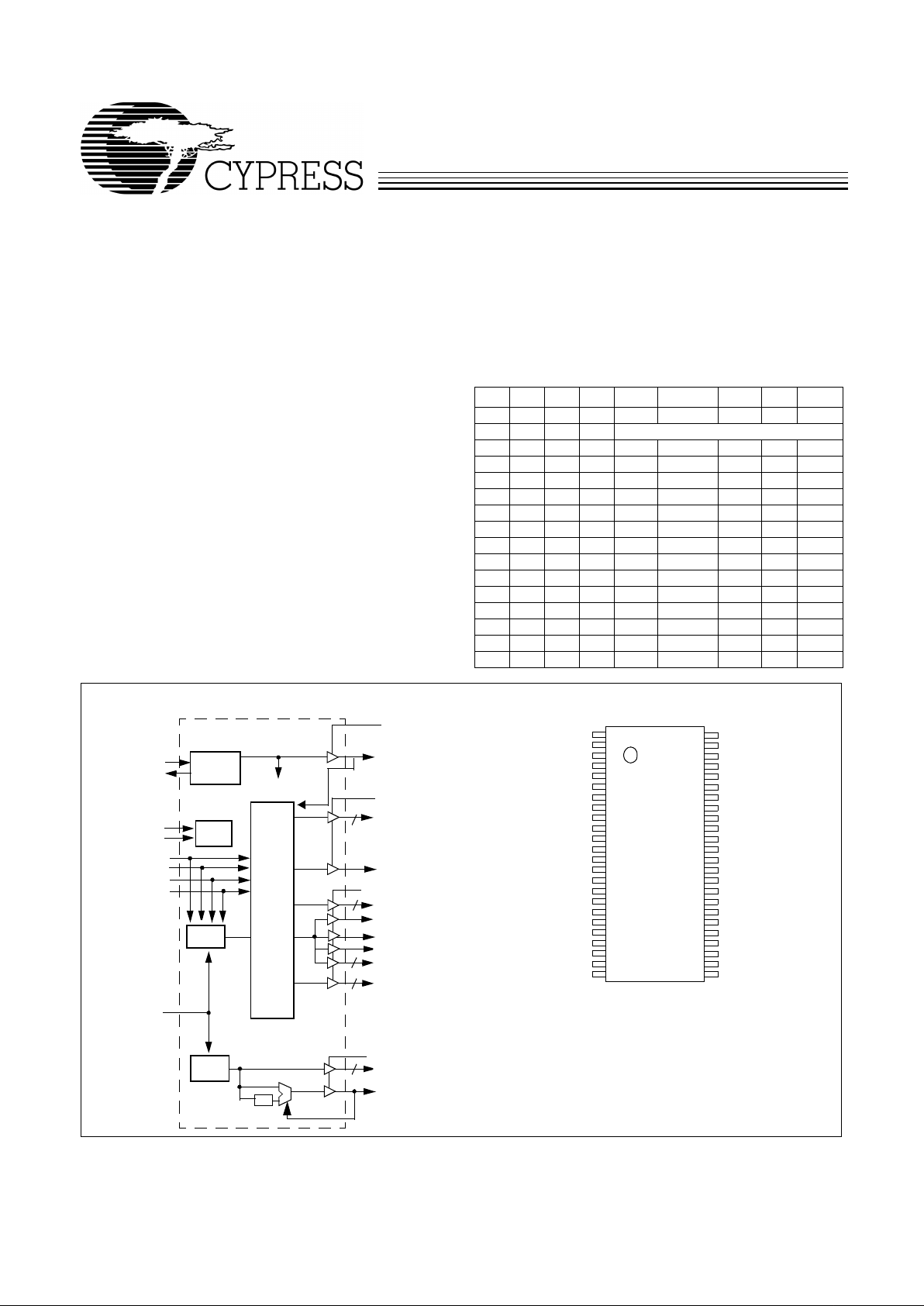
Block Diagram
Pin Configuration
VDDQ3
VDDQ2
PCI1/FS1*
XTAL
PLL REF FREQ
PLL 1
X2
X1
REF2X/FS3*
PCI3:7
48MHz_0:1
SI0/24_48#MHz*
PLL2
OSC
VDDQ3
I2C
SDATA
Logic
SCLK
3V66_0:1
CPU0:1
APIC
Divider,
Delay,
and
Phase
Control
Logic
2
VDDQ3
2
SDRAM0:8
9
PWRDWN#
PCI0/FS0*
PCI2/FS2*
/2
FS3*
FS2*
FS1*
FS0*
5
2
REF2x/FS3*
VDDQ3
X1
X2
GND
VDDQ3
3V66_0
3V66_1
GND
FS0*/PCI0
FS1^/PCI1
FS2*/PCI2
GND
PCI3
PCI4
VDDQ3
PCI5
PCI6
PCI7
GND
48MHz_0
48MHz_1
SI0/24_48#MHz*
VDDQ3
W195B
VDDQ2
APIC
VDDQ2
CPU0
CPU1
GND
VDDQ3
SDRAM0
SDRAM1
SDRAM2
GND
SDRAM3
SDRAM4
SDRAM5
VDDQ3
SDRAM6
SDRAM7
SDRAM8
GND
PWRDWN#*
SCLK
VDDQ3
GND
SDATA
48
47
46
45
44
43
42
41
40
39
38
37
36
35
34
33
32
31
30
29
28
27
26
25
1
2
3
4
5
6
7
8
9
10
11
12
13
14
15
16
17
18
19
20
21
22
23
24
Note:
1. Internal 250K pull-up or pull down resistors present on inputs
marked with * or ^ respectively. Design should not rely solely on
internal pull-up or pull down resistor to set I/O pins HIGH or LOW
respectively.
[1]

W195B
PRELIMINARY
2
Pin Definitions
Pin Name Pin No.
Pin
Type Pin Description
REF2x/FS3 1 I/O
Reference Cloc k with 2x Dri ve/Frequ ency Select 3:
3.3V 14.318-MHz cl ock out put. This pin also serves as the select s trap to det ermine device operating f requency
as described in Table 1.
X1 3 I
Crystal Input:
This pin has dual functi ons. It can be used as an ext ernal 14.318-
MHz crystal connectio n or as an external reference frequency input .
X2 4 I
Crystal Output:
An input connection for an external 14.318-MHz crystal connec-
tion. If using an external reference, this pin must be left unconnected.
PCI0/FS0 10 I/O
PCI Clock 0/Frequency Selecti on 0:
3.3V 33-MHz PCI cloc k outputs. This pi n also
serves as the s elect st rap t o determine de vic e opera ti ng fre quency as desc ribed i n
Table 1.
PCI1/FS1 11 I/O
PCI Clock 1/Frequency Selecti on 1:
3.3V 33-MHz PCI cloc k outputs. This pi n also
serves as the s elect st rap t o determine de vic e opera ti ng fre quency as desc ribed i n
Table 1.
PCI2/FS2 12 I/O
PCI Clock 2/Frequency Selection 2:
3.3V 33-MHz PCI clock outputs. This pin
doubles as the sel ect strap to determine device operating frequency as described
in Table 1.
PCI3:7 14, 15, 17, 18, 19O
PCI Clock 3 t hrough 7:
3.3V 33-MHz PCI cl ock o utputs. PCI0 :7 can be i ndividual ly
turne d of f vi a I
2
C interface.
3V66_0:1 7,8 O
66-MHz Clock Outp ut:
3.3V output clocks. The operating frequency is controlled
by FS0:3 (see Table 1).
48MHz_0:1 21, 22 O
48-MHz Clock Outp ut
: 3.3V fixed 48-MH z, non-spread spectrum clock output.
SIO/
24_48#MHz
23 I/O
Clock Output for Super I/O:
This is the input clock for a Super I/O (SIO) device.
During power- up, it also se rves as a selection st rap. I f it is sampled HIGH, the output
frequency for SIO is 24 MHz. If the input is sampled LOW, the output is 48 MHz.
PWRDWN# 29 I
Power Down Control:
LVTTL-compatible input that places the device in power-
down mode when held LO W.
CPU0:1 45, 44 O
CPU Clock Outputs:
Clock output s for the host bus interface. Output frequencies
depending on the configuration of FS0:3. Voltage swing is set by V
DDQ2
.
SDRAM0:8, 41, 40, 39, 37,
36, 35, 33, 32, 31O
SDRAM Clock Outputs:
3.3V outputs for SDRAM. The operating frequency is
controlled by FS0:3 (see Table 1).
APIC 47 O
Synchronous APIC Clock Outputs:
Clock outputs running synchronous with the
PCI clock outputs. Voltage swing set by V
DDQ2
.
SDATA 25 I/O Da ta pi n for I
2
C circuitry .
SCLK 28 I Clock pin for I
2
C circuitry.
VDDQ3 2, 6, 16, 24, 27,
34, 42
P
3.3V Pow er Connection:
Po wer supply fo r SDRAM output buff ers, PCI output buff -
ers, ref erence output buffers, and 48-MHz output buffers. Connect to 3.3V.
VDDQ2 46, 48 P
2.5V Pow er Connection:
Po wer supply for IOAPIC and CPU output buffers . Con-
nect to 2.5V or 3.3V.
GND 5, 9, 13, 20, 26,
30, 38, 43
G
Ground Connections:
Connect all ground pins to the common system ground
plane.

W195B
PRELIMINARY
3
Overview
The W195B is a highly integrated frequency timing gener ator,
supplying all the required clock sources for an Intel® architecture platform using graphics in tegrated core logic.
Functional Description
I/O Pin Operation
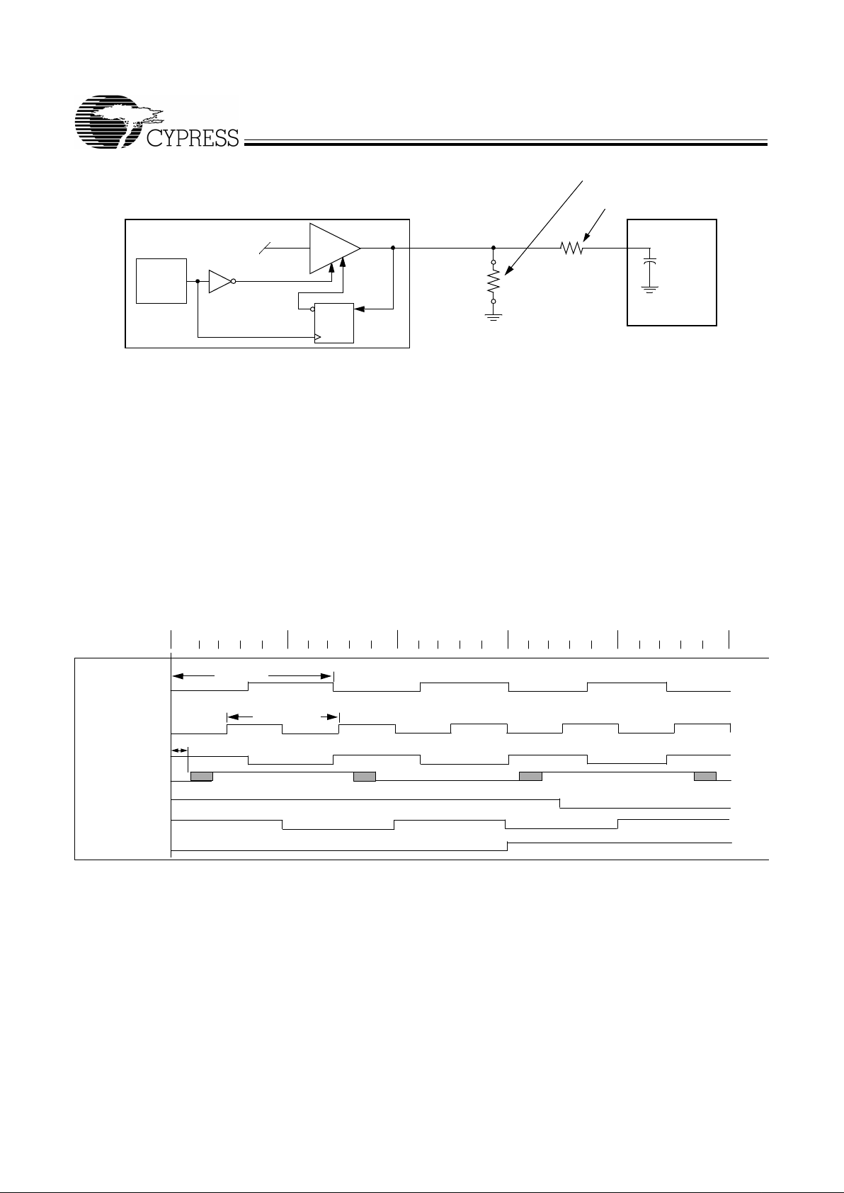
Pin # 1, 10, 11, 12, 23 ar e dual -purpose l/ O pi ns. Up on po werup the pin acts as a logic input. An external 10-kΩ strapping
resistor sho uld be used. Figure 1 shows a s ugges te d meth od
for strapping resistor connections.
After 2 ms, the pin becomes an output. Assuming the power
supply has stabilized by then, the specified output frequency
is delivered on the pins. If the power supply has not yet
reached full value, output freq uency initiall y m ay be below target but will increase to target once supply voltage has stabilized. In either case, a short output clock cycle may be produced from the CPU clock outputs when the outputs are
enabled.
Offsets Among Clock Signal Groups
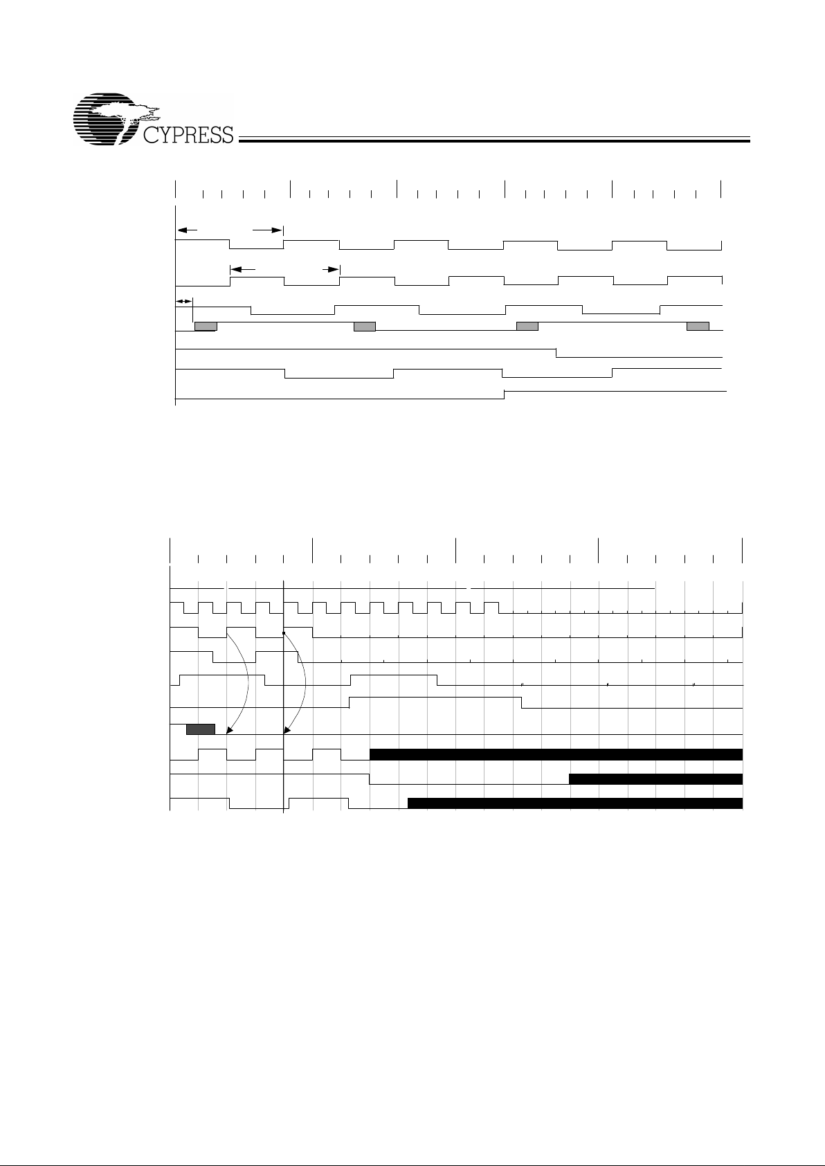
Figure 2 and Fi gure 3 r epresent the p hase relat ionshi p among
the different groups of clock outputs from W195B when it is
providing a 66-MHz CPU clock and a 100-MHz CPU clock,
respectively. It should be noted that when CPU clock is operating at 100 MHz, CPU clock output is 180 degrees out of
phase with SDRAM clock outputs.
Figure 1. Input Logic Selection Through Resistor Load Option
Power-on
Reset
Timer
Output Three-st ate
Data
Latch
Hold
QD
W195B
Clock Load
Output
Buffer
10 k
Ω
Output
Low
Output Strapping Resistor
Series T ermination Resistor
Figure 2. Group Offset Wa veforms (66.8 CPU Clock, 100.2 SDRAM Clock)
CPU 66-MHz
SDRAM 100-MHz
3V66 66-MHz
PCI 33-MHz
REF 14.318-MHz
USB 48-MHz
APIC
0 ns 10 ns
CPU 66 Period
SDRAM 100 Period
Hub-PC
40 ns30 ns 20 ns

W195B
PRELIMINARY
4
Power Down Control
W195B prov ides one PWRDWN# signal to p lace the device in lo w-power mode. In low-pow er mode, the PLLs are turned of f and
all clock outputs are driven LOW.
Notes:
2. Once the PWRDWN# signal is sampled LOW for two consecutive rising edges of CPU clock, clocks of interest should be held LOW on the next HIGH-to-LOW
transition.
3. PWRDWN# is an asynchronous input and metastable conditions could exist. This signal is synchronized inside W195B.
4. The shaded sections on the SDRAM, REF, and USB clocks indicate “don’t care” states.
5. Diagrams shown with respect to 100 MHz. Similar operation when CPU is 66 MHz.
Figure 3. Group Offset Waveforms (100.2 CPU Clock, 100.2 SDRAM Clock)
CPU 100-MHz
SDRAM 100-MHz
3V66 66-MHz
PCI 33-MHz
REF 14.318-MHz
USB 48-MHz
APIC
0 ns
SDRAM 100 Period
CPU 100 Period
Hub-PC
40 ns30 ns20 ns10 ns
Figure 4. PWRDWN# Timing Diagram
[2, 3, 4, 5]
1 2
Center
0ns 25ns 50ns 75ns
VCO Internal
CPU 100MHz
3V66 66MHz
PCI 33MHz
APIC
PwrDwn
SDRAM 100MHz
REF 14.318MHz
USB 48MHz
 Loading...