Cypress W170-01 Datasheet

W170-01
Spread A ware ™, F reque ncy Multi plier and Zero Del ay Buffe r
Features
• Spread Aware ™—desi gned to work with SSFTG
reference signals
• T wo outputs
• Configuration options allow various multiplication of
the reference frequency, refer to
Table 1
to deter mine
the specific option which meets your multi p lication
needs
• Available in 8-pin SOIC package
Key Specific ati o n s
Operatin g Voltage: ........ .. .......... ....... 3 .3V±5% o r 5. 0 V ± 10 %
Operating Range: ... ........... .. .......20 MHz < f
OUT1
< 133 MHz
Absolute Jitter: .........................................................±500 ps
Output to Output Skew: ................. ............................. 250 ps
Propagation Delay: ......................................... .. .. ......±350 ps
Propagation delay is affected by input rise time.
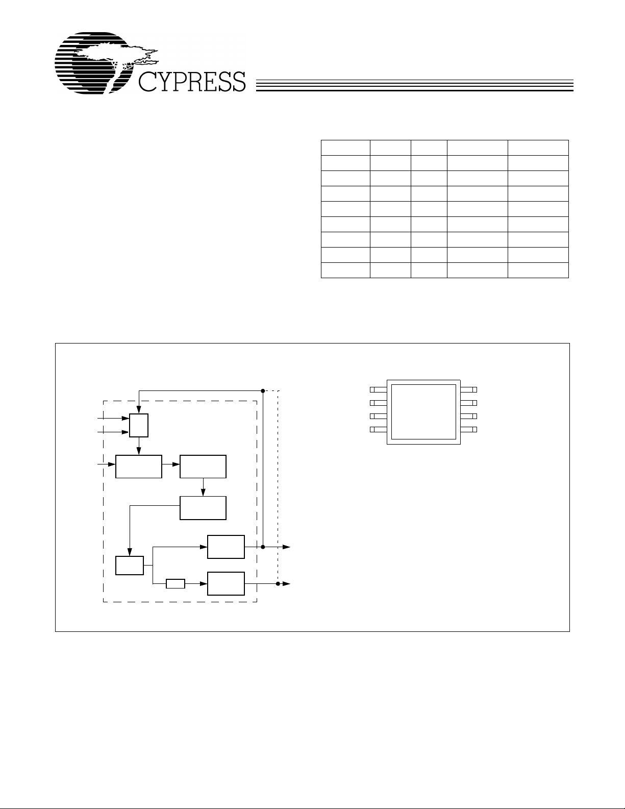
Block Diagram
External feedback connection to
OUT1 or OUT2, not both
FS0
FS1
FBIN
÷Q
T able 1. Configuration Options
FBIN FS0 FS1 OUT1 OUT2
OUT1 0 0 2 X REF REF
OUT1 1 0 4 X REF 2 X REF
OUT1 0 1 REF REF/2
OUT1 1 1 8 X REF 4 X REF
OUT2 0 0 4 X REF 2 X REF
OUT2 1 0 8 X REF 4 X REF
OUT2 0 1 2 X REF REF
OUT2 1 1 16 X REF 8 X REF
Pin Configuration
FBIN
IN
GND
FS0
1
2
3
4
8
7
6
5
OUT2
VDD
OUT1
FS1
IN
Reference
Input
Spread Aware is a trademark of Cypress Semiconductor Corporation.
Phase
Detector
VCO
÷2
Charge
Pump
Loop
Filter
Output
Buffer
Output
Buffer
OUT1
OUT2
Cypress Semiconductor Corporation
• 3901 North First Street • San Jose • CA 95134 • 408-943-2600
September 28, 1999, r ev . **

Pin Definitions
Pin Name Pin No.
IN 2 I
FBIN 1 I
OUT1 6 O
OUT2 8 O
VDD 7 P
GND 3 P
FS0:1 4, 5 I
Pin
Type Pin Description
Reference Input:
Feedback Input:
ensure proper func ti onality. If the trac e between FBIN and the output pin being used
for feedback is equal in length to the traces bet ween the outputs and the signal destinations, then t he si gnals re ceiv ed at the dest inations will be synchroni z ed to the REF
signal input (IN).
Output 1:
back signal connected to FBIN, and the FS0:1 inputs (see Table 1).
Output 2:
of OUT1. See Table 1.
Power Connections:
0.1-µF decoupling capacitor. Use ferrite beads to help reduce noise for optimal jitter
performance.
Ground Connection:
Function Select Inputs:
T able 1.
The frequency of the signal provided by this pin is determined by the feed-
The frequency of th e signal provi ded by this pin is one- half of the fr equency
The output signals will be synchronized to this signal.
This input must be fed by one of the outputs (OUT1 or OUT2) to
Connect to 3.3V or 5V. Thi s pi n should be bypassed with a
Connect all grounds to the common system ground plane.
Tie to VDD (HIGH, 1) or GND (LOW, 0) as desired per
W170-01
Overview
The W170-01 is a two-output zero delay buffer and frequency
multiplier. It pro vides an e xternal fee dbac k path all owing maximum flexibility when implementing the Zero Delay feature.
This is explained further in the sec tions of thi s d ata she et ti tle d
“How to Implement Zero Delay,” and “Inserting Othe r D evices
in Feedback Path. ”
The W170-01 is a pin-compatible upgrade of the Cypress
W42C70-01. The W170-01 addresses some application dependent problems experienced by users of the older device.
Most importantly, it addresses the tracking skew problem induced by a reference whic h has Spread Spectrum Timin g enabled on it.
Spread Aware
Many systems being designed n ow utilize a technology called
Spread Spectrum Fr equency Timing Gener ation. Cypress has
been one of the pioneers of SSFTG devel opment , and we designed this product so as not to filter off the Spread Spectrum
feature of the Ref erence input, assu ming it exists. When a zero
delay buffer is not designed to pass the SS feature through,
the result is a significant amount of tracking skew which may
cause problems in systems requiring synchronization.
For more details on Spread Spectrum timing technology,
please see the Cypr ess application note titled, “EMI Suppression Techniques with Spread Spectrum Frequency Timing
Generator (SSFTG) ICs.”
2
 Loading...