

Cypress W164G Datasheet
Spread Spectrum Desktop/Notebook System
Frequenc y Generato r
W164
Cypress Semiconductor Corporation
• 3901 North First Street • San Jose • CA 95134 • 408-943-2600
December 16, 1999, rev. **
Features
• Maximized EMI suppression usi ng Cypress’s Spread
Spec t r u m techno logy
• Reduces measured EMI by as much as 10 dB
•I
2
C programmabl e to 153 MHz (16 sel ectable
frequencies)
• T wo skew-controll ed copies of CPU output
• SEL100/66# selects CPU frequency (100 or 66.8 MHz)
• Seven copies of PCI output (synchronous w/CPU
output)
• One copy of 14.31818-MHz IOAPIC output
• One copy of 48-MHz USB output
• Selectable 24- /48-MHz output is determined b y resistor
straps on power-up
• One high-drive outpu t buffer that pr oduces a copy of
the 14.318-MHz reference
• Isolated core VDD pin for noise reduction
Key Specifications
Supply Voltages:....... ........... .......... .. .........V
DDQ3
= 3.3V±5%
V
DDQ2
= 2.5V±5%
CPU Cy cl e to Cyc le Jitter:............ .. .......... ... .. .......... .. ..2 0 0 p s
CPU, PCI Output Edge Rate:
.........................................≥
1 V/ns
CPU0: 1 O u tp u t Skew : .. ... .. .......... .. ... .......... .. ..............175 ps
PCI_ F, PCI1:6 O ut p u t Skew: .................. .. ... ......... ... .. ..50 0 p s
CPU to PCI Skew: ..............................1 to 4 ns (CPU Leads)
REF2X/SEL48#, SCLOCK, SDATA. ........... .. ..250-kΩ pull-up
Note:
Internal pull-up resistors should not be relied upon for
setting I/O pins HIGH.
T able 1. Pin Selectable Frequency
SEL100/66# CPU(0:1) PCI
1 100 MHz 33.3 MHz
0 66.8 MHz 33.4 MHz
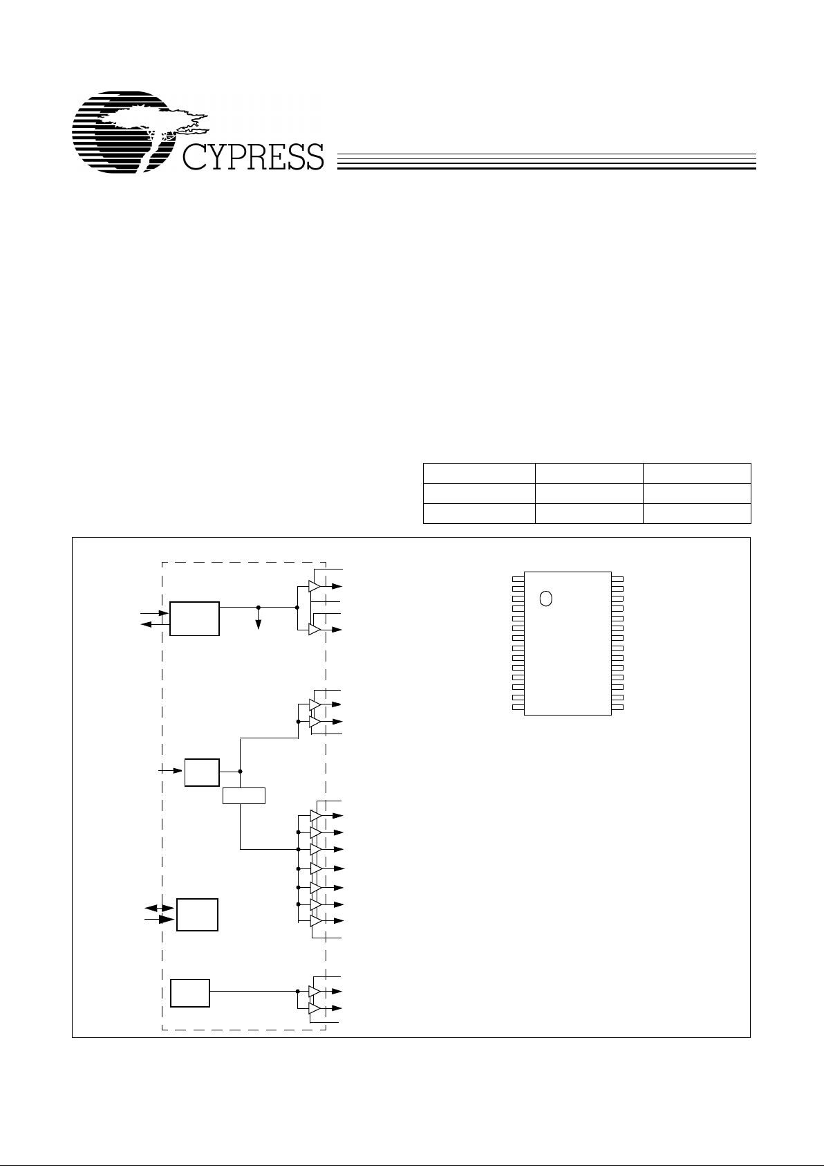
Pin ConfigurationBlock Diagram
X1
X2
GND
PCI_F
PCI1
PCI2
PCI3
PCI4
VDDQ3
PCI5
PCI6
VDDQ3
48MHz
24/48MHz
GND
REF2X/SEL48#
VDDQ3
VDDQ2
IOAPIC
VDDQ2
CPU0
CPU1
VDDQ3
GND
SDATA
SCLOCK
SEL100/66#
GND
28
27
26
25
24
23
22
21
20
19
18
17
16
15
1
2
3
4
5
6
7
8
9
10
11
12
13
14
VDDQ3
REF2X/SEL48#
VDDQ3
IOAPIC
CPU0
CPU1
PCI_F
XTAL
PLL Ref Freq
PLL 1
100/66#_SEL
X2
X1
VDDQ3
PCI1
PCI2
PCI3
PCI4
PCI5
48MHz
24/48MHz
PLL2
OSC
VDDQ2
PCI6
GND
GND
VDDQ3
GND
GND
I2C
SCLOCK
SDATA
LOGIC
÷2/÷3/÷4
W164
2
Functional Description
I/O Pin Operation
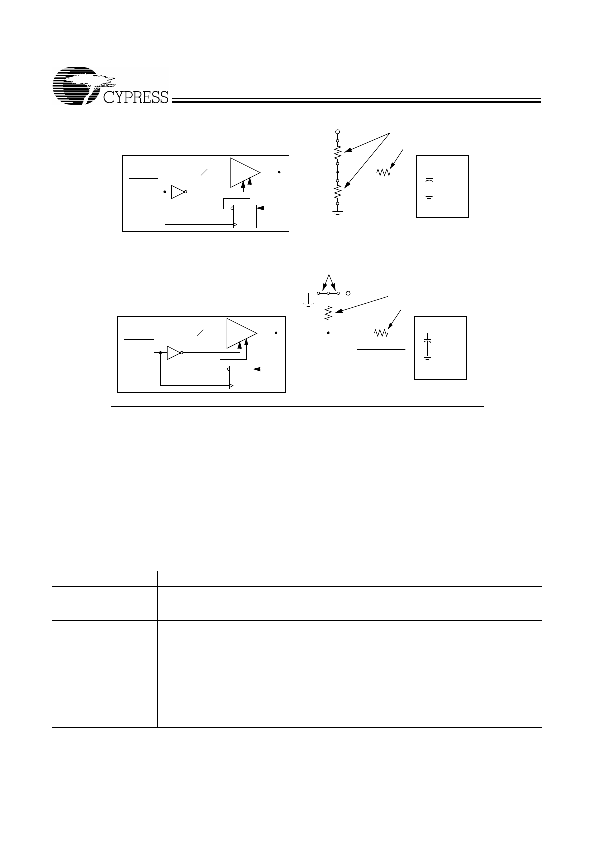
Pin 27 is a dual-purpose l/O pin. Upon power-up this pin acts
as a logic i nput, a llo wing the determinat ion of assigne d de vic e
functions . A short time after pow er-up , the logic state of th e pin
is latched and the pin becomes a clock output. This feature
reduces devi ce pin count by combi ning clock out puts with input
select pins .
An external 10-kΩ “strapping” resistor is connected between
the l/O pin and ground or V
DD
. Connection to ground sets a
latch to “0,” connection to V
DD
sets a latch to “1.” Fig ure 1 an d
Figure 2 show two suggested methods for strapping resistor
connections.
Upon W164 power-up, the first 2 ms of operation is used for
input logic selection. During this period, the Reference clock
output buffer is three-stated, allowing the output strapping resistor on the l /O pin to pu ll the pi n and its as sociated c apacitiv e
clock load to either a logic HIGH or LOW state. At the end of
the 2-ms period , the esta blishe d logic “0” or “1” condition of the
l/O pin is then latched. Nex t the output buffer is enabl ed which
converts the l/O pin into an operating clock output. The 2-ms
timer is started when V
DD
reaches 2.0V. The input bit can onl y
be reset by turning V
DD
off and then back on again.
It should be noted tha t the stra ppi ng resi stor has no si gnifi cant
effect on clock output signal integrity. The drive impedance of
clock output is 25Ω (nominal) which is minimally affected by
the 10-kΩ strap to ground or V
DD
. As with th e se r ie s termi n ation resistor, the output strap pin g resist or should be placed as
close to the l/O pin as possible in order to keep the interconnecting trace short. The trace from the resistor to ground or
V
DD
should be kept less than two inches in length to prevent
system noise coupli ng duri ng input logic sampling.
When the clock output is en abled fo llowing the 2-m s input pe-
riod, a 14.318-MHz output frequency is delivered on the pin,
assuming that V
DD
has stabilized. If VDD has not yet reached
full value , output frequency initi ally ma y be belo w target b ut will
increase to target once V
DD
voltage has stabilized. In either
case, a short output clock cycle may be produced from the
CPU clock outputs when the outputs are enabled.
Pin Definitions
Pin Name
Pin
No.
Pin
Type Pin Description
CPU0:1 22, 21 O
CPU Clock Output s 0 thr ough 1:
These two CPU clo c ks run at a freque ncy s et by
SEL100/66#. Output voltage s wing is set by the voltage applied to VDDQ2.
PCI1:6
PCI_F
5, 6, 7, 8, 10,
11, 4
O
PCI Clock Outputs 1 thr ough 6 and PCI_F:
These se ven PCI clock out puts run
synchronously to the CPU clock. Voltage swing is set by the power connection to
VDDQ3.
IOAPIC 24 O
I/O APIC Clock Output:
Provides 14. 318-MHz fi xed fr equ ency. The output voltage
swing is set by the power connec ti on to VDDQ2.
48MHz 13 O
48-MHz O u tput:
Fixed 48-MHz USB clock. Output voltage swing is controlled by
voltage applied to VDDQ3.
24/48MHz 14 O
24-MHz or 48-MHz Output:
Frequency is set by the state of pin 27 on power-up.
REF2X/SEL48# 27 I/O
I/O Dual-Function REF2X and SEL48# pin:
Upon power-up, the state of SEL48#
is latched. The initial state is set by either a 10K resistor to GND or to V
DD
. A 10K
resistor to GND causes pin 14 to output 48 MHz. If the pin is strapped to V
DD
, pin
14 will output 24 MHz. Afte r 2 ms , the pin becomes a high -drive out put that produces
a copy of 14.318 MHz.
SEL100/66# 16 I
Frequency Selecti on Input:
Selects CPU clock frequency as shown i n Table 1 on
page 1.
SDATA 18 I/O
I
2
C Data Pin:
Data should be presented to thi s input as described in the I
2
C section
of this data sheet. Internal 250-kΩ pull-up resistor.
SCLOCK 17 I
I
2
C Clock Pin:
The I
2
C data cloc k sho uld be pr esented to thi s input as describe d in
the I
2
C section of this data shee t.
X1 1 I
Crystal Connection or External Reference Frequency Input:
Connec t to eit h er
a 14.318-MHz crystal or other reference signal.
X2 2 I
Crystal Connection:
An input connection for an ext ernal 14.318-MHz crystal. If
using an external referen ce, this pin must be lef t unconnected.
VDDQ3 9, 12, 20, 26 P
Po wer Connection:
P ower s upply f or core log ic and PL L circuit ry , PCI , 48-/24- MHz,
and Reference output buffers. Connect to 3.3V supply.
VDDQ2 23, 25 P
Po we r Connection:
Power supply for IOAPIC and CPU output buffers. Connect to
2.5V supply.
GND 3, 15, 19, 28 G
Ground Connection s:
Connect all ground pins to the common system ground
plane.
W164
3
Serial Data Interface
The W164 features a two-pi n, serial data interface that can be
used to configure internal register settings that control particular de vice funct ions. Upon power -up , the W164 i nitiali zes wit h
default register settings. Therefore, the use of this serial data
interface is optional. The serial interface is write-only (to the
clock chi p) and i s the dedi cated f unc tion of de v ice pi ns SDAT A
and SCLOCK. In motherboard applications, SDATA and
SCLOCK are typically driven by two logic outputs of the
chipset. Clock device register changes are normally made
upon system initialization, if required. The interface can also
be used during system ope ration f or pow er management functions. Table 2 summarizes the control functions of the serial
data interface.
Operation
Data is written to the W164 in ten bytes of eight bits each.
Bytes are written in the order sho w n in Table 3.
Power-on
Reset
Timer
Outp ut T h re e-stat e
Data
Latch
Hold
QD
W164
V
DD
Clock Lo ad
10 k
Ω
Output
Buffer
(Load O p ti o n 1)
10 k
Ω
(Load O p ti o n 0)
Output
Low
Output Strapping Resistor
Series Termination Resistor
Figure 1. Input Logic Selection Through Resistor Load Option
Power-on
Reset
Timer
Output Three-state
Data
Latch
Hold
QD
W164
V
DD
Clock Load
R
10 k
Ω
Output
Buffer
Output
Low
Output Strapping Resistor
Series Termination Resistor
Jumper Options
Resistor Value R
Figure 2. Input Logic Selection Through Jumper Option
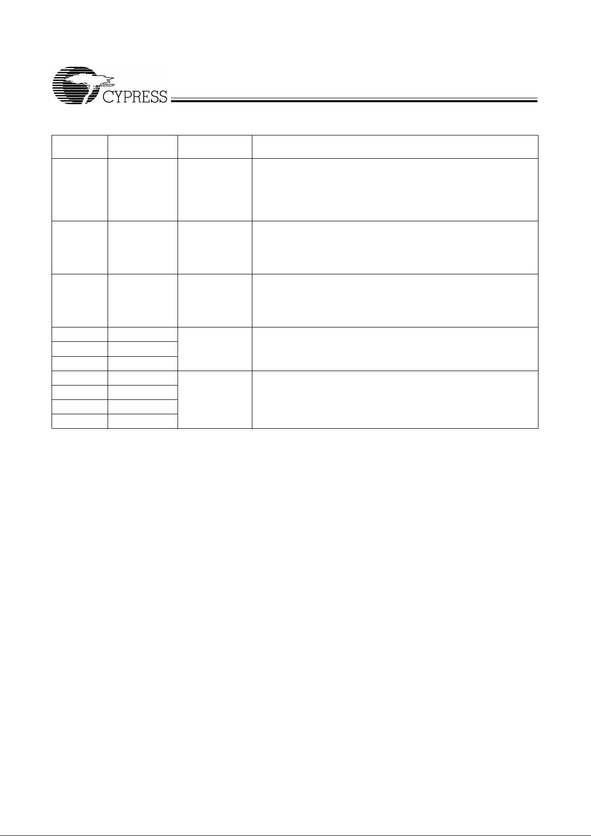
T able 2. Serial Data Interface Contr ol Functions Summary
Control Function Description Common Application
Clock Output Disable Any indivi dual cloc k output(s) can be disabled. Dis-
abled outputs ar e actively held LOW.
Unused outputs are di sabled to reduce EMI
and system power. Examples are clock outputs to unused PCI slots.
CPU Clock Fr equency
Selection
Provides CPU/PCI fr equency selections be yond the
100- and 66.6-MHz sel ecti ons t hat ar e provi ded by
the SEL100/66# pin. Frequency is chan ged in a
smooth and controlled fashion.
For alternate microprocessors and power
management options . Smooth freque ncy transition allows CPU frequency change under
normal system operation.
Output Three-state Puts all clock outputs into a high-impedance state. Production PCB testing.
T es t Mode All cl ock out puts t oggle i n rela tion t o X1 inp ut, i nter-
nal PLL is bypassed. Refer to Table 4.
Production PCB testing.
(Reserved) Reserved functio n for future device re vision or pro-
duc tion device testing.
No user application . Regist er bit must be wri t-
ten as 0.
W164
4
Table 3. Byte Writing Sequence
Byte
Sequence Byte Name Bit Sequence Byte Description
1 Slave Address 11010010 Commands the W164 to accept the bit s in Data Bytes 3–6 for internal
register configuration. Since other devices may exist on the same common serial data bus , i t is necessary to have a specific slave address for
each potential receiver. The slave receiv er address fo r the W164 is
11010010. Register setting will not be made if the Sla ve Address is not
correct (or is for an alternate slave receiver).
2 Command
Code
Don’t Care Unused by the W164 , therefor e bit value s are ignored ( “don’t care”). This
byte must be inc luded in the data write seq uence to main tain proper by te
allocation. The Command Code Byte is part of the standard serial communication pr otocol and may be used when writ ing to another addressed
slave receiver on the serial data bus.
3 Byte Count Don’t Care Unused by the W164 , therefor e bit val ues are ignored ( “don’t care”). This
byte must be inc luded in the data write seq uence to main tain proper by te
allocation. The Byt e Count Byte is part of the standard serial communication proto col and may b e used when writi ng to another addre ssed sla ve
receiver on the serial data bus.
4 Data Byte 0 Don’t Care Refer to Cypress SDRAM drivers.
5 Data Byte 1
6 Data Byte 2
7 Data Byte 3 Refer to Table 4 The data bits in these byt es set internal W164 registers that cont rol device
operation. The data bits are only accepted when the Address Byte bit
sequence is 11010010, as noted above. For description of bit control
functions, refer to Table 4, Data Byte Serial Configuration Map.
8 Data Byte 4
9 Data Byte 5
10 Data Byte 6
 Loading...