Cypress W163-15, W163-05 Datasheet

Spread Aware™, Zero Delay Buffer
W163
Cypress Semiconductor Corporation
• 3901 North First Street • San Jose • CA 95134 • 408-943-2600
February 21, 2000, re v. *A
Features
• Spread Aware™—designed to work with SSFTG
reference signals
• Outputs may be three-stated
• Available in 8-pin SOIC package
• Extra strength output drive available (-15 version)
• Internal feedback maximized the number of outputs
available in 8-pin package
Key Specifications
Operating Voltage: ................................................3.3V±10%
Operating Range: ................................ 10 < f
OUT
< 133 MHz
Cycle-to-Cycle Jitter: ..................................................200 ps
Output-to-Ou tp u t S kew: ... .......... ......... .......... .......... ....250 p s
Device-to-Device S kew:...... .......... .......... ......... ............700 p s
Propagation Delay:......................................................350 ps
Spread Aware is a trademark of Cypress Semiconductor Corporati on.
Block Diagram
Pin Configuration
Q0
PLL
REF
Q1
Q2
Q3
QFB
QFB
VDD
8
7
6
5
REF
Q0
Q1
GND
1
2
3
4
Q3
Q2
SOIC

W163
2
Overview
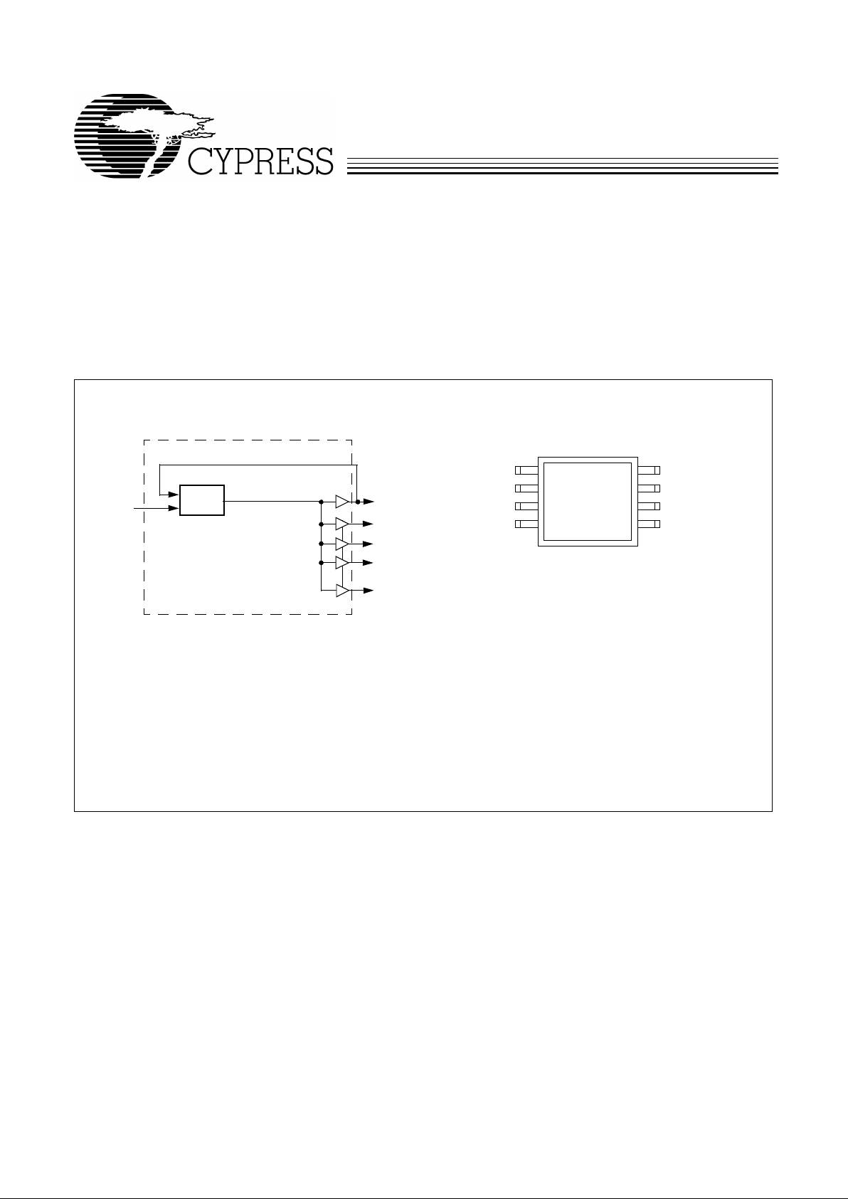
The W163 products are five-output zero delay buffers. A
Phase-Lock ed Loop (PLL) i s used to tak e a time- varying signal
and provide five copies of that same signal out. The internal
feedback to the PLL provides outputs in phase with the reference inputs.
Spread Aware
Many syst em s being designed now util ize a technology called
Spread Spectrum F requency Timi ng Generation . Cypress has
been one of the pioneers of SSFTG development, and we designed this product so as not to filter off t he Spread Spectrum
featur e of the Referen ce input, assuming i t ex ists. When a z ero
delay buffer is not designed to pass the SS feature through,
the result is a significant amount of tracking skew which may
cause problems in systems requiring synchronization.
For more details on Spread Spectrum timing technology,
please see the Cypress Applic ation not e titled , “EMI Suppression Techniques with Spread Spectrum Frequency Timing
Generator (SSFTG) ICs.”
Schematic
Pin Definitions
Pin Name Pin No.
Pin
Typ e Pin Description
REF 1 I
Reference Input:
The output signals Q0:3 will be synchronized to this signal
unless the device is programmed to bypass the PLL.
Q0:3 2, 3, 5, 7 O
Outputs:
These signal s will be synchronous a nd of equal f requency t o the signal
input at pin 1.
QFB 8 O
Feedback Output:
This output signal does no t vary from signal s Q0:3 in func tion,
but is noted as the signal used to establish the propagation delay of nearly 0.
VDD 6 P
Po we r Connections:
Connect to 3.3V. Use ferrite beads to help reduce noise
for optimal jit te r p e rformance.
GND 4 P
Ground Connections:
Connect all grounds to the common system ground
plane.
Q0
Q1
GND
QFB
Q3
VDD
Q2
V
DD
Ferrite
Bead
10
µ
F0.1 µF
REF
 Loading...